1. Introduction
In recent years, AlGaN-based deep ultraviolet light-emitting diodes (DUV LEDs) have undergone rapid development and have been widely applied in numerous fields, including water and air purification, medical equipment, food sterilization [
1], UV detection [
2,
3,
4,
5], optical wireless communication (OWC), and so on [
6,
7,
8,
9,
10]. Compared with conventional mercury lamps, DUV LEDs have significant advantages such as their being pollution-free, their long service lifetime, their low operating voltage, their compact size, and their high frequency modulation capability [
11,
12]. Nevertheless, these emerging applications impose extremely stringent performance requirements on DUV LEDs, particularly in terms of light output power (LOP) density and efficiency. As a result, the fabrication of high-performance DUV LEDs still faces numerous challenges, among which, non-uniform current spreading and low light extraction efficiency (LEE) are the most prominent bottlenecks [
13,
14,
15]. In this context, Micro-LEDs have attracted considerable attention recently, owing to their great potential to overcome these limitations and improve the optical and electrical performance of DUV devices.
Micro-LEDs could operate at higher current density because of uniform current spreading and rapid heat dissipation capability [
16]. Up to now, multiple research groups have attempted to further boost the performance of DUV Micro-LEDs by reducing the emission area. Tian et al. demonstrated that an inclined sidewall could enhance LEE from the bottom sapphire by reflecting the emitted light downward. Moreover, the LOP density of these Micro-LEDs exceeded 40 W/cm
2, with a corresponding 19% enhancement in EQE [
17]. Zhang et al. verified that Micro-LED arrays with localized surface plasmon resonance (LSPR) could increase the electroluminescence (EL) intensity significantly, achieving an LOP density of approximately 8 W/cm
2 and an EQE of approximately 3% [
18]. Li et al. proposed a parallel-arrayed planar strategy to improve the LOP of Micro-LEDs, achieving a peak LOP density of 66.8 W/cm
2 at a current density of 1150 A/cm
2 [
19]. Very recently, Yu et al. reported that a triangular-mesa DUV Micro-LED exhibited a 29% enhancement in LOP density, reaching 74 W/cm
2, with a peak EQE of ~1.35% [
20]. Despite these substantial advances, the LOP density of state-of-the-art DUV Micro-LEDs is still insufficient to meet the demand of high-power DUV applications, calling for further optimization of device performance.
In this work, we fabricated and characterized flip-chip AlGaN-based DUV Micro-LEDs with ultra-high LOP density. Each Micro-LED pixel was isolated by a SiO2 layer to suppress inter-pixel crosstalk, and a novel covering metal layer was employed to interconnect individual pixels for independent addressing, which simultaneously improved the current spreading uniformity. Numerical finite-difference time-domain (FDTD) calculations revealed that the LEE of transverse-electric (TE) polarized light for the Micro-LEDs was markedly enhanced by 68% compared with conventional large-area DUV LEDs. Experimentally, the peak EQE of the Micro-LEDs was enhanced by 24.6%, while the EQE at peak LOP density was improved by 35.7%. More importantly, the fabricated devices achieved a record-high LOP density of 77.1 W/cm2 under direct-current (DC) operation at a high current density of 2.3 kA/cm2, representing a 605% enhancement compared with conventional low-power DUV LEDs.
2. Device Structure and Fabrication
The AlGaN-based LED epitaxial wafer used in this work was grown on a 2-inch c-plane sapphire substrate by metal–organic chemical vapor deposition (MOCVD). The epitaxial wafer of the DUV LED consisted of a 2.3 µm AlN layer, a 1.5 µm thick n-doped Al0.65Ga0.35N layer, a 1 µm thick n-doped Al0.6Ga0.4N layer, 3 periods of 3 nm thick Al0.7Ga0.3N/12 nm thick Al0.5Ga0.5N multiple quantum wells (MQWs), a 40 nm thick Al0.8Ga0.2N electron blocking layer (EBL), a 15 nm thick p-AlGaN layer with a graded Al composition decreasing from 0.75 to 0.35, and a 2 nm thick p-GaN cap layer.
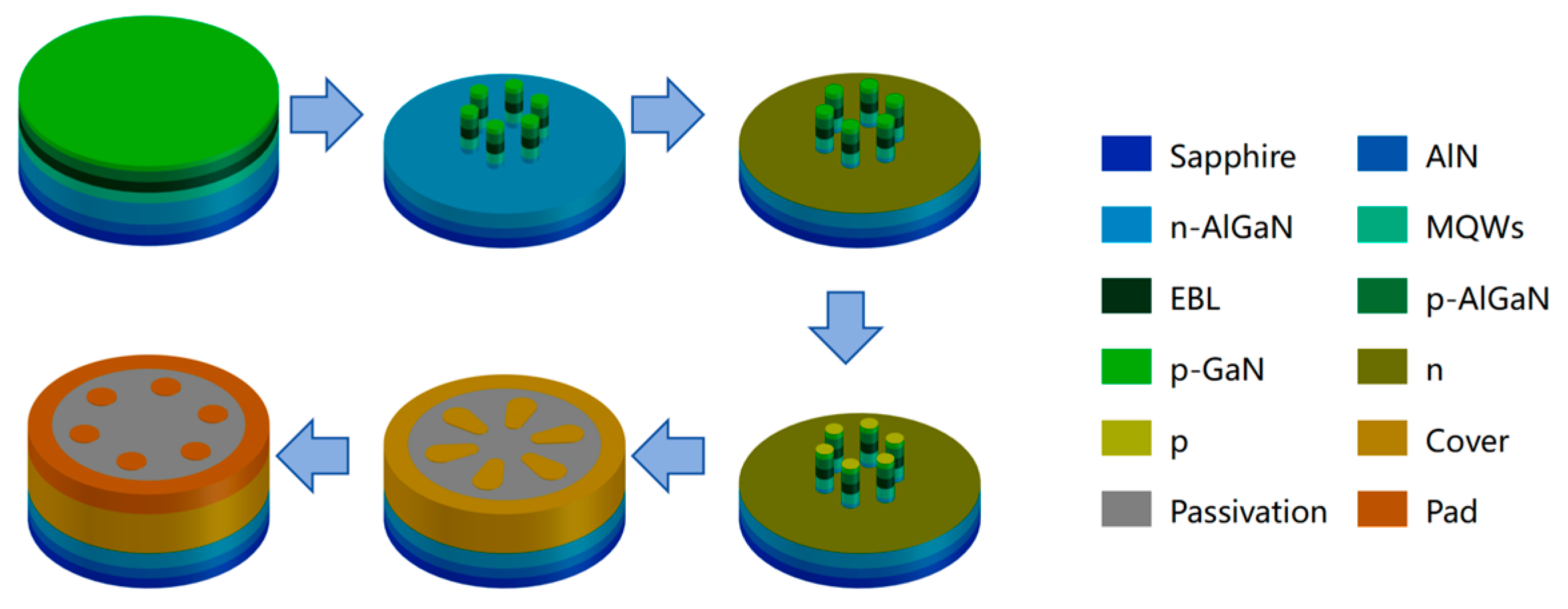
The fabrication process is depicted in
Figure 1. Standard photolithography and inductively coupled plasma (ICP) etching were performed to form mesas of 50 μm diameter, which terminated at the n-AlGaN layer (800 nm). Next, a room temperature KOH etching solution was then conducted for approximately 30 min to remove plasma damage induced by ICP etching. Subsequently, Cr/Ti/Al/Ni/Au/Ti multi-layers were deposited as the n-type electrode surrounding the mesas, and a rapid thermal annealing (RTA) process at 800 °C was employed to form the ohmic contact. Similarly, Ni/Au/Ni/Rh/Ti multi-layers were deposited as the p-type electrode and then rapidly annealed at 600 °C to form the ohmic p-contact. Following this, a roughly 1 μm thick SiO
2 layer was deposited as the insulating layer using plasma-enhanced chemical vapor deposition (PECVD). Then, the SiO
2 passivation layer above both the p-type electrode and the 100 μm wide annular n-electrode was etched by ICP to obtain the via holes. Furthermore, Ti/Pt/Au covering layers were deposited to optimize the electrical characteristics and interconnect the Micro-LEDs. After depositing another 1 μm thick SiO
2 passivation layer and forming the via holes, 4.7 μm thick Au/Sn metal pads were deposited as the electrode pads of the Micro-LEDs. Finally, the sapphire substrate was thinned down to facilitate light extraction, and light was emitted through the transparent sapphire substrate.
All optical and electrical measurements were performed on the bare and unpackaged Micro-LED dies. The EL spectra were measured using an Ocean Optics USB2000+ spectrometer (Ocean Optics, Orlando, FL, USA). The optical measurements of the Micro-LED were carried out using a calibrated Labsphere SC6000 radiometer (Labsphere, North Sutton, NH, USA), with a Si photodetector (Labsphere, North Sutton, NH, USA) in close proximity to the polished sapphire substrate of the Micro-LED. The I-V characteristics were measured by using a Keithley 2460 Source Meter (Tektronix, Beaverton, OR, USA).
3. Results and Discussion
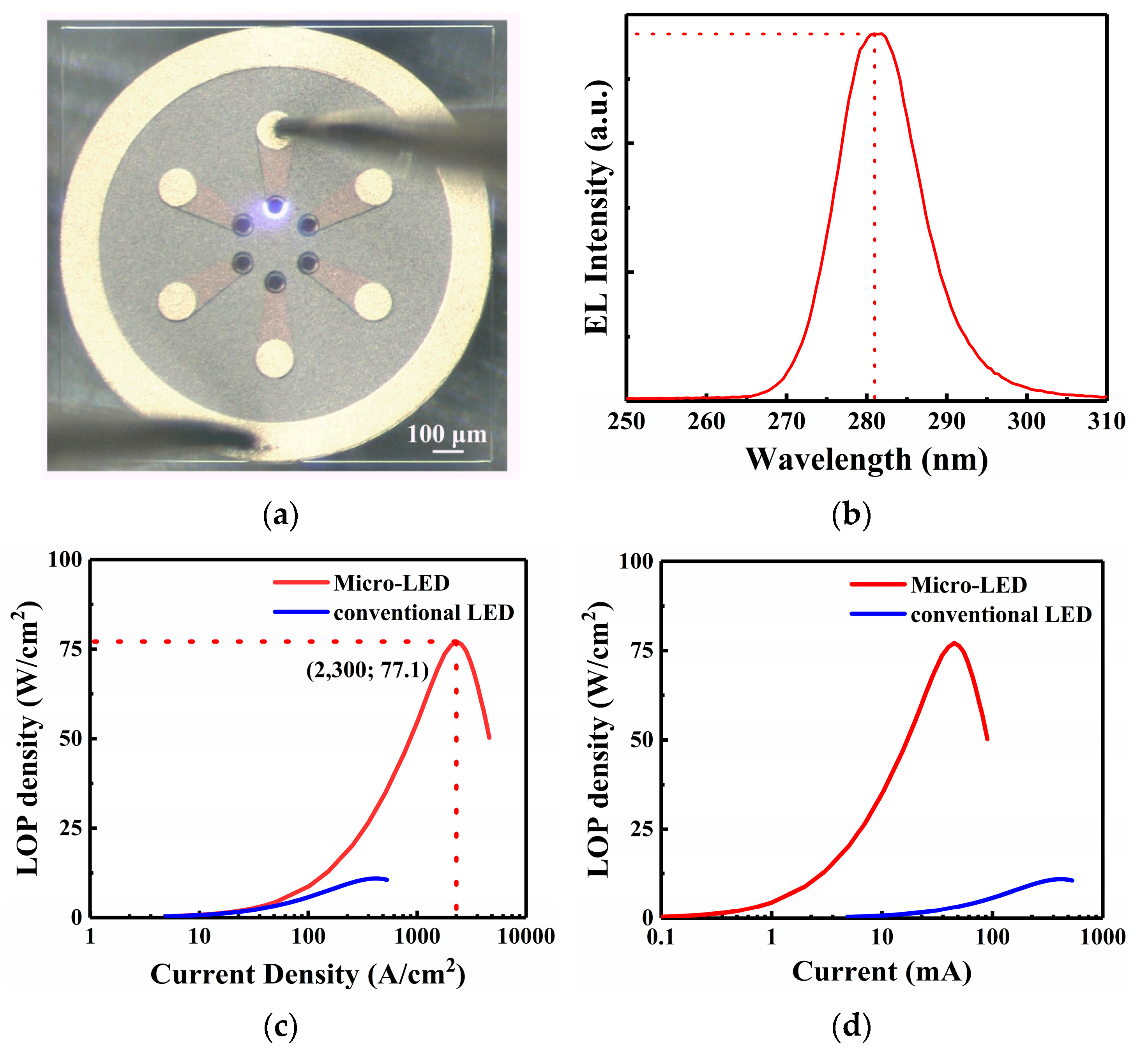
Figure 2a shows the optical image of the fabricated Micro-LEDs with a diameter of 50 µm at 40 mA current in this work. With a common shared cathode, each Micro-LED pixel can be individually addressed by its corresponding anode.
Figure 2b shows the EL spectrum of the Micro-LED. The peak emission wavelength of the Micro-LED device is approximately 281 nm at 40 mA current.
Figure 2c,d shows the LOP density–current density and LOP density–current curves of the Micro-LED and the conventional LED, respectively. Notably, the emission area of this conventional LED is nearly 31 times that of a Micro-LED, measuring approximately 60,543 μm
2 and 1963 μm
2, respectively. It can be seen that the maximum measured LOP density of the Micro-LED is 77.1 W/cm
2 at 2.3 kA/cm
2 current density, corresponding to an LOP of 1.51 mW. The conventional DUV LED achieves a peak LOP density of 10.93 W/cm
2 at 429.4 A/cm
2, beyond which the LOP density gradually declines. In contrast, the Micro-LED exhibits a 605% enhancement in peak LOP density of up to 77.1 W/cm
2 at a high current density of 2.3 kA/cm
2 compared to the conventional DUV LED. This enhancement is attributed to the improved LEE and the current-spreading characteristics induced by Micro-LEDs. We believe that the LOP density improvement benefits from both the micro-size effect and the improvement in LEE.
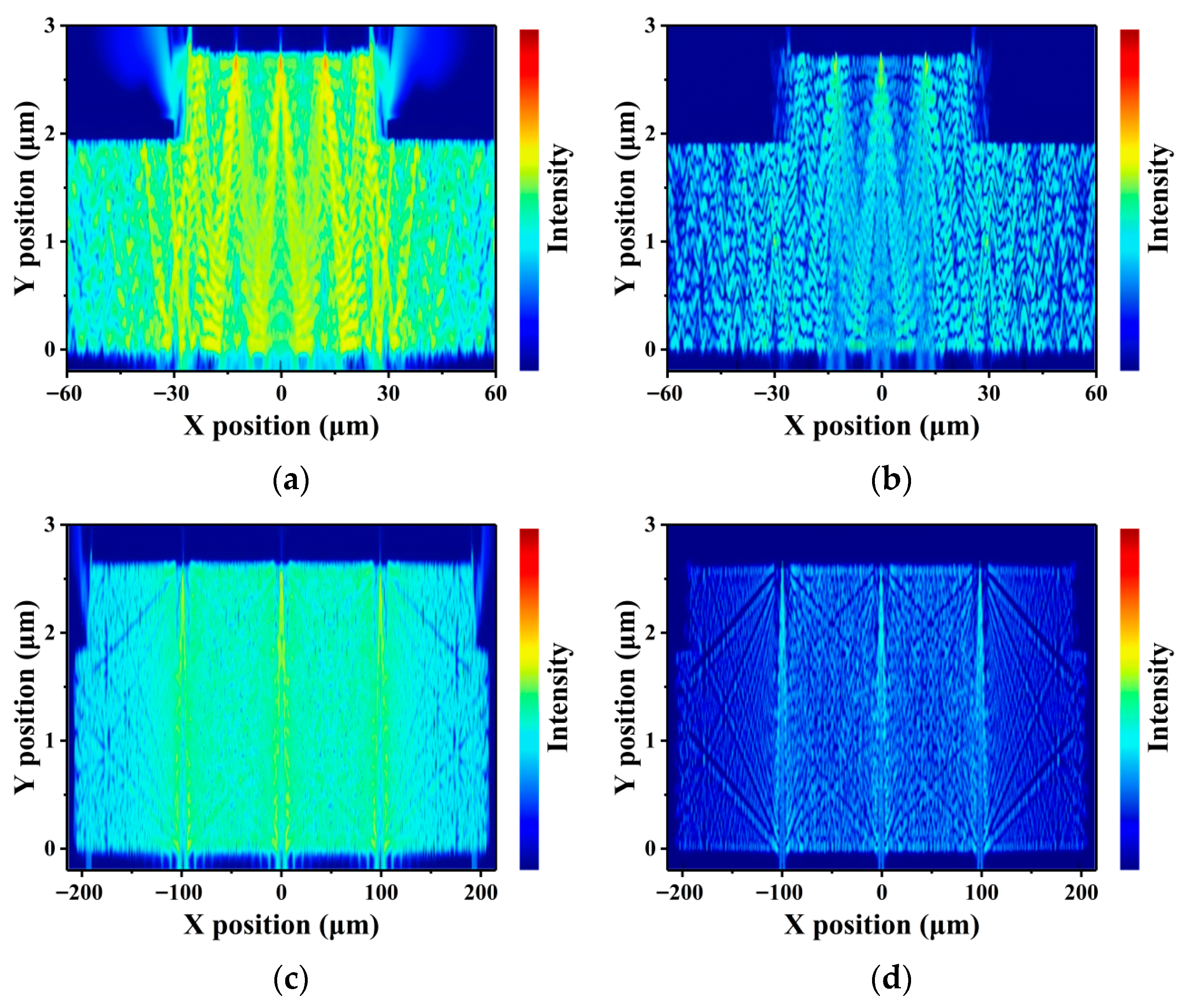
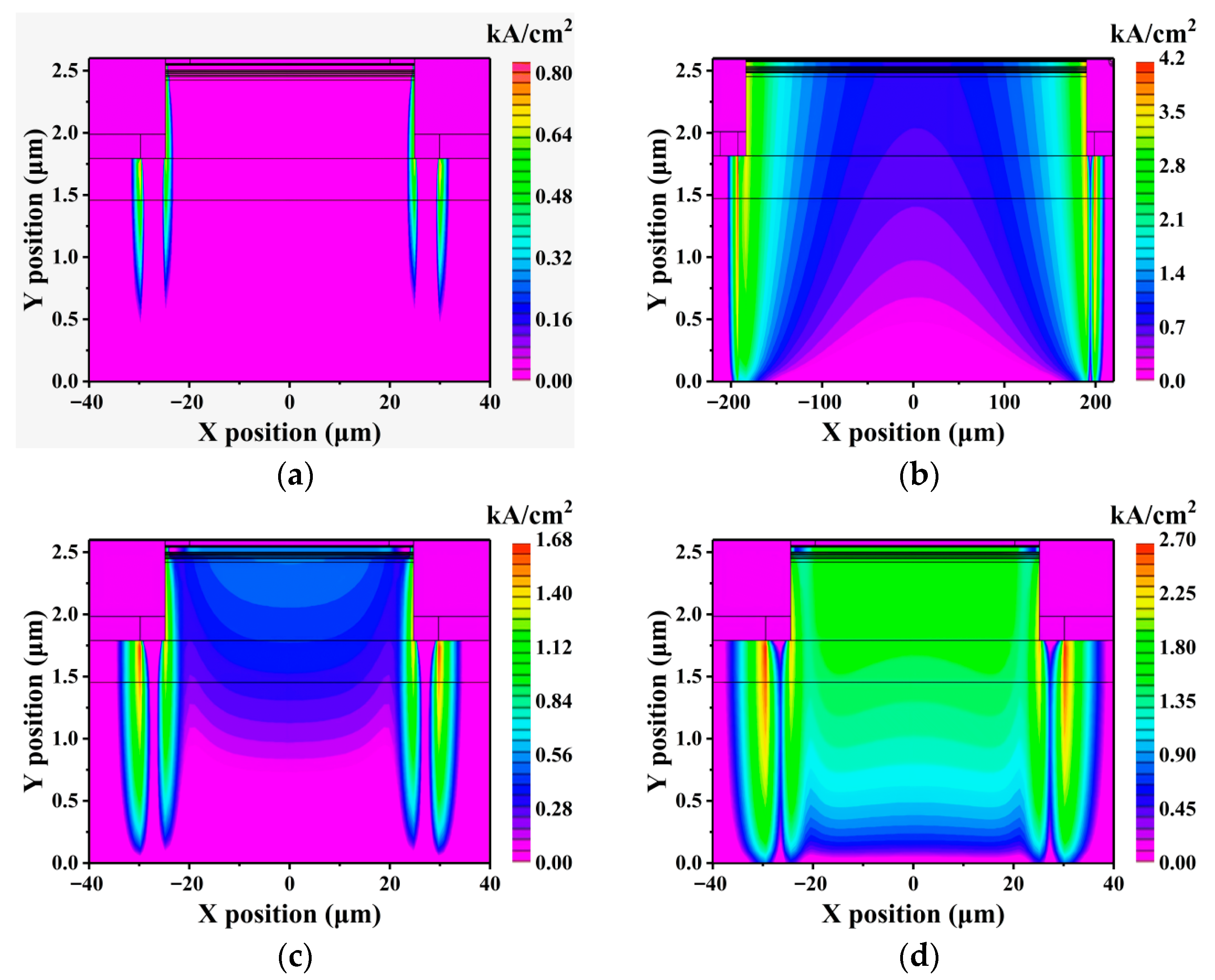
The core goal of the simulation is to perform a relative comparison of the optical performance between the two types of devices. The simulation models of the Micro-LED and the conventional LED were simplified to reduce model complexity and improve simulation efficiency. All simulations were performed in a 2D domain, and three dipole light sources were uniformly distributed within MQWs. A perfectly matched layer (PML) was used for all boundary conditions. The dipole’s polarization direction parallel to the plane containing the quantum well was defined as the TE polarization mode, while the perpendicular polarization was defined as the TM polarization mode. The refractive indices of the p-GaN, p-AlGaN, EBL, MQWs, and n-AlGaN were 2.596, 2.596, 2.3, 2.597, and 2.56, respectively. The electric field distributions of this Micro-LED are shown in
Figure 3a,b. TE-polarized light enhancement includes both bottom-out and sidewall-out emissions. TM-polarized light mainly enhances sidewall-out emission. It can be seen that the LEEs of TE-polarized and TM-polarized light are 24.73% and 39.18%, respectively.
Figure 3c,d shows the electric field distributions for TE-polarized light and TM-polarized light of the conventional LED. It can be seen that the LEEs of TE-polarized and TM-polarized light are 14.69% and 37.98%, respectively. Compared with the conventional LED, the LEEs of TE-polarized and TM-polarized light for the Micro-LED are enhanced by 68% and 3.2%, respectively, which can be attributed to the enhanced emission from both the sidewall and the bottom surfaces. The photon transmission distance becomes shorter from the emission region to the sidewall, making it easier for DUV light to escape from the sidewall. It is revealed that part of the DUV light that originally underwent total internal reflection (TIR) within the device is successfully refracted out of the Micro-LED. By contrast, more DUV light experiences total internal reflection, and only a small fraction of DUV light can be extracted in the conventional LED.
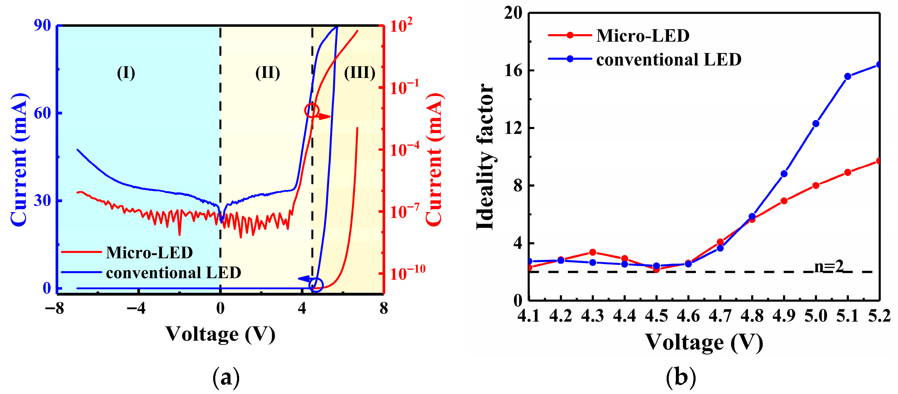
Figure 4a shows the current-voltage (I-V) characteristics of the Micro-LED and the conventional LED. The I-V characteristics were measured using a Keithley 2460 Source Meter. The logarithmic I-V curves can be divided into three main regions: the reverse bias region I; the low-forward bias region II (0 V to 4.5 V); and the high-forward bias region III above the turn-on voltage. In the reverse bias region I, the conventional LED exhibits an extremely low leakage current of 10
−9 A, while the Micro-LED demonstrates an even lower leakage current of 10
−10 A. This can be attributed to the reduction in the active region volume and sidewall area, as well as effective sidewall passivation. In region II, the current increases below the threshold voltage.
Figure 4b shows the dynamic ideality factor (n-V) curves of the Micro-LED and the conventional LED; the minimum values of ideality factor n were 2.17 (Micro-LED) and 2.41 (conventional LED), respectively. Both values are greater than 1, indicating that Shockley–Read–Hall (SRH) nonradiative recombination plays an important role in both devices. Although sidewall recombination dominates, the Micro-LED exhibits a lower leakage current compared to the conventional LED. This also indicates that the superior passivation process we adopted has effectively reduced sidewall defects. The ideality factor of the Micro-LED is close to 2, reflecting a potentially more uniform current distribution than in the conventional LED. In region III, the Micro-LED exhibits a higher voltage at the same current, mainly due to two factors: (i) series resistance is inversely proportional to the square of the LED’s diameter, and (ii) the Micro-LED in this work has a longer current spreading path.
The cross-sectional current density distributions of the Micro-LED and the conventional LED are compared in
Figure 5a,b. Both simulations were performed under nearly identical injection conditions, corresponding to an average current density of 500 A/cm
2. One can see that the distribution in the conventional LED is extremely non-uniform, with the peak current density approaching 4.2 kA/cm
2 at the edge of the n-contact. This is a manifestation of strong current crowding in the conventional LED, a phenomenon that is effectively absent in the Micro-LED.
Figure 5c,d shows the current density distributions of the Micro-LED at 40 mA and 100 mA, respectively. At the high injection current density of 100 mA, the Micro-LED still maintains a highly uniform current distribution, which is attributed to the reduction in size that has shortened the lateral current spreading distance.
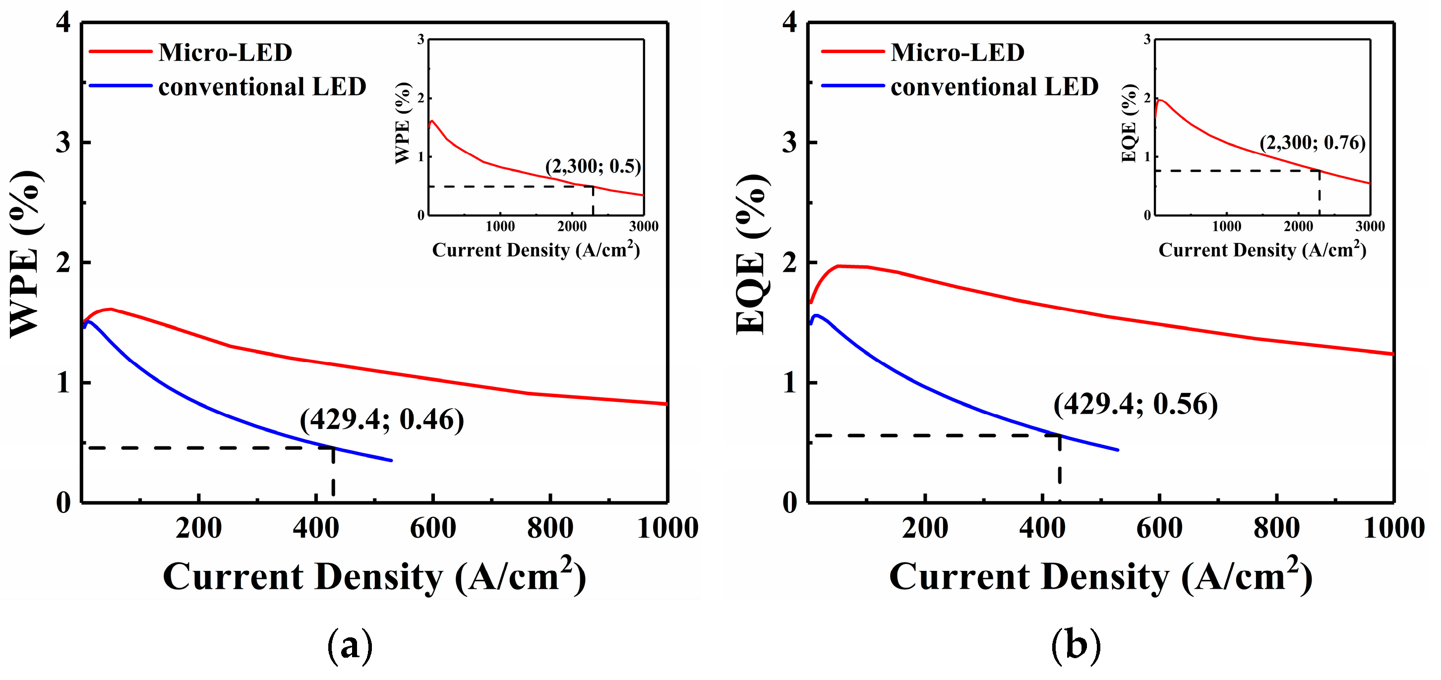
Figure 6a shows the relationship between WPE and current density. WPE represents the efficiency of converting input electrical energy into output optical energy. The peak WPE values of the Micro-LED and the conventional LED are approximately 1.61% and 1.50%, respectively. As the current density increases, the WPE of the Micro-LED decreases more slowly than that of the conventional LED. The WPE of the Micro-LED and the conventional LED at the peak LOP density are 0.5% and 0.46%, respectively. Compared with the conventional LED, the peak WPE and WPE at the peak LOP density of the Micro-LED are enhanced by 7.3% and 8.7%, respectively.
Figure 6b shows the EQE characteristics of the Micro-LED and the conventional LED versus current density. The peak EQE values of the Micro-LED and the conventional LED are approximately 1.96% and 1.56%, and the EQE values of the Micro-LED and the conventional LED at the peak LOP density are 0.76% and 0.56%, respectively. The peak EQE and the EQE at peak LOP density for the Micro-LED are enhanced by 24.6% and 35.7%, respectively, which can be attributed to the LEE enhancement for the Micro-LED.
With the increasing current density, the EQE values of both devices also show a decreasing trend, similar to that of WPE. The WPE enhancement of the Micro-LED is lower compared to that of EQE, which can be attributed to the design of Micro-LEDs. Specifically, the injected current must first flow through the electrode covering layer to the central p-type electrode before being collected by the n-type electrode at the outer ring-shaped pad. In other words, the Micro-LEDs in this design have a longer lateral current path. As the series resistance is proportional to the length of the current path, the Micro-LEDs exhibit a larger series resistance, leading to additional electrical power dissipation in the resistive layers.
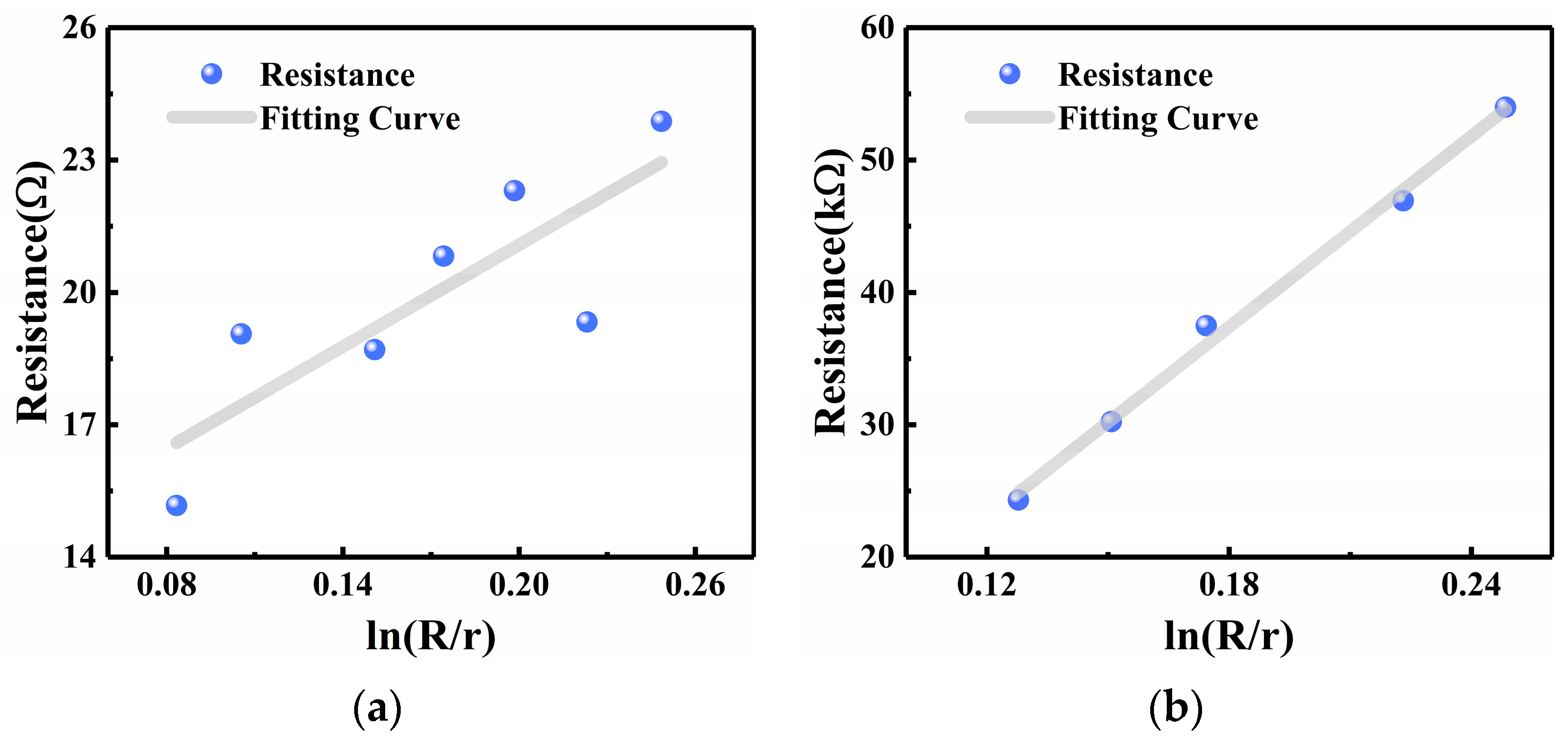
The circular transmission line model (CTLM) was employed to evaluate the ohmic contact quality and estimate the specific contact resistivity. By fitting the linear relationship between ln(R/r) and the resistance of the concentric rings, the specific contact resistivity can be obtained, as shown in
Figure 7a,b. The specific contact resistivities of the n-type and p-type CTLM contacts of the Micro-LEDs are 7.314 × 10
−4 Ω·cm
2 and 2.203 × 10
−2 Ω·cm
2, respectively. These results confirm that the Micro-LEDs in this work exhibit excellent ohmic contact performance.




 ,
,