3.1. Synthesis of the TiNx Diffusion Barrier
In advanced PV contact systems, multilayer stacks such as Si/TiSi
2/TiN/Cu are considered to be highly attractive. A key challenge is understanding the formation of Ti–Si phases (TiSi
2, Ti
5Si
3, Ti
5Si
4, etc.) during rapid or prolonged thermal treatments, since these phases largely determine the contact resistivity and stability [
25,
26]. A particularly relevant question concerns the feasibility of depositing TiN directly onto Si, forming a Si/TiN
x interface and subsequently annealing at 700–800 °C without an initial Ti layer or intentional silicide formation [
14,
27]. Whether such processing conditions lead to the spontaneous formation of conductive Ti–Si phases, or whether TiN can maintain its integrity as a diffusion barrier under these temperatures, remains insufficiently understood. This uncertainty extends to more complex barrier schemes, such as SiC
x/TiN bilayers, where the combined thermal stability, interlayer reactions, and Cu diffusion-blocking behavior have not yet been systematically clarified [
26,
28].
Thus, to ensure the formation of an effective TiN-based diffusion barrier, the presence of a TiSi2 ohmic interlayer at the TiN/substrate interface is essential. Therefore, this section investigates the potential of spontaneous formation of a TiSi2 layer at the Si/TiN interface during TiN deposition and subsequent annealing. Particular attention is given to assessing whether such interfacial reactions can occur without the intentional introduction of a metallic Ti layer during the sputtering process, which would significantly simplify the fabrication route and reduce process complexity.
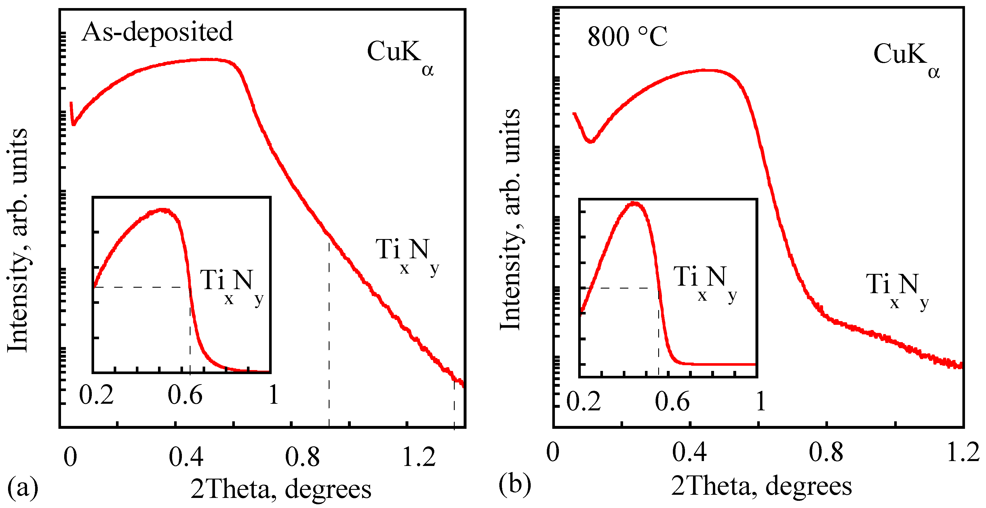
To determine the thickness and density of the deposited TiN films, XRR measurement was employed. The measurements were carried out before and after annealing at 800 °C in order to assess structural changes, densification effects, and possible interfacial reactions induced by high-temperature treatment. The corresponding experimental results are presented in
Figure 2.
Figure 2 presents the XRR curves of TiN films on Si before and after annealing. In the as-deposited state, the film exhibits clear Kiessig fringes, with periodic oscillations in the XRR curve extending to approximately 2.5° in 2θ. These fringes indicate a smooth, uniform film with well-defined thickness, while the sharp drop in intensity at 0.639° marks the critical angle of total external reflection. The regular periodicity and high amplitude of the fringes confirm excellent interface quality between the TiN layer and the Si substrate. After annealing at 800 °C in Ar for 30 min, the critical angle shifts to 0.556°, indicating a reduction in film density. The Kiessig fringes are strongly suppressed and scarcely visible, consistent with increased surface roughness and interfacial degradation caused by thermal decomposition and agglomeration. Insets show the same data plotted on linear intensity scales. In
Figure 2 the X-axis represents the 2θ angle in degrees, while the Y-axis corresponds to X-ray intensity in arbitrary units, displayed on logarithmic scales in the main plots and linear scales in the insets.
Analysis of the XRR curves shows that the as-deposited TiN films exhibit a critical angle of total external reflection of 0.639° in
Table S1. According to density calculations, this value corresponds to approximately 5.131 g/cm
3, suggesting the formation of a Ti
60N
40 (Ti
3N
2) composition with an excess of titanium atoms relative to stoichiometric TiN. The film thickness extracted from the periodicity of the Kiessig fringes was estimated to be about 244 nm in
Table S2.
The results of measuring the XRR spectra of TiN films after annealing at 800 °C in Ar are shown in
Figure 2b. A pronounced reduction in the TiN film density is evident from the XRR data after annealing. The post-annealing critical angle, 2θ
s = 0.556°, corresponds to a calculated density of 3.89 g/cm
3 in
Table S3, substantially lower than both metallic titanium (4.54 g/cm
3) and stoichiometric TiN (5.44 g/cm
3). Such a decrease indicates significant structural and compositional modifications induced by the 800 °C thermal treatment. This density reduction is consistent with the possible formation of lower-density Ti–Si phases such as TiSi (4.03 g/cm
3), Ti
5Si
4 (4.26 g/cm
3), and Ti
5Si
3 (4.32 g/cm
3), which can arise as a result of interfacial reactions between TiN and Si during high-temperature annealing. In addition, variations in surface morphology and topography make a significant contribution to the apparent density reduction. AFM characterization in
Figure S1 revealed that the initially uniform nanocrystalline surface of TiN films transforms during annealing at 700 °C and 750 °C into large surface agglomerates measuring 300–400 nm, comparable to the film thickness. These agglomerates gradually decrease in size to about 50 nm after 700–800 °C annealing. As a result, the film exhibits a pyramidal microstructure with pronounced surface deformation and distinct voids between adjacent features. These voided regions effectively decrease the average density probed by XRR, consistent with the measured value of 3.89 g/cm
3 in
Table S3.
The pronounced surface roughness also prevented reliable extraction of the film thickness from the XRR spectra. The pyramidal morphology suppresses Kiessig fringes and attenuates the primary reflection, rendering standard thickness fitting impossible. Such suppression of interference oscillations is a well-established consequence of increased surface roughness and interfacial heterogeneity in XRR analysis.
To investigate the evolution of the structural properties during annealing, XRD measurements were performed in
Figure S2. The results indicate that TiN nanocrystals are formed immediately after deposition, as evidenced by the continuous diffraction rings observed in the photographic film. Reflections corresponding to seven crystallographic planes of TiN were identified, namely TiN (111), (200), (220), (311), (222), (331), and (420) [
29,
30].
To assess changes in the phase composition, the Debye diffraction patterns were analyzed by comparing the relative positions of the X-ray reflections in the as-deposited state and after annealing at 700 °C, 750 °C, and 800 °C for 30 min in
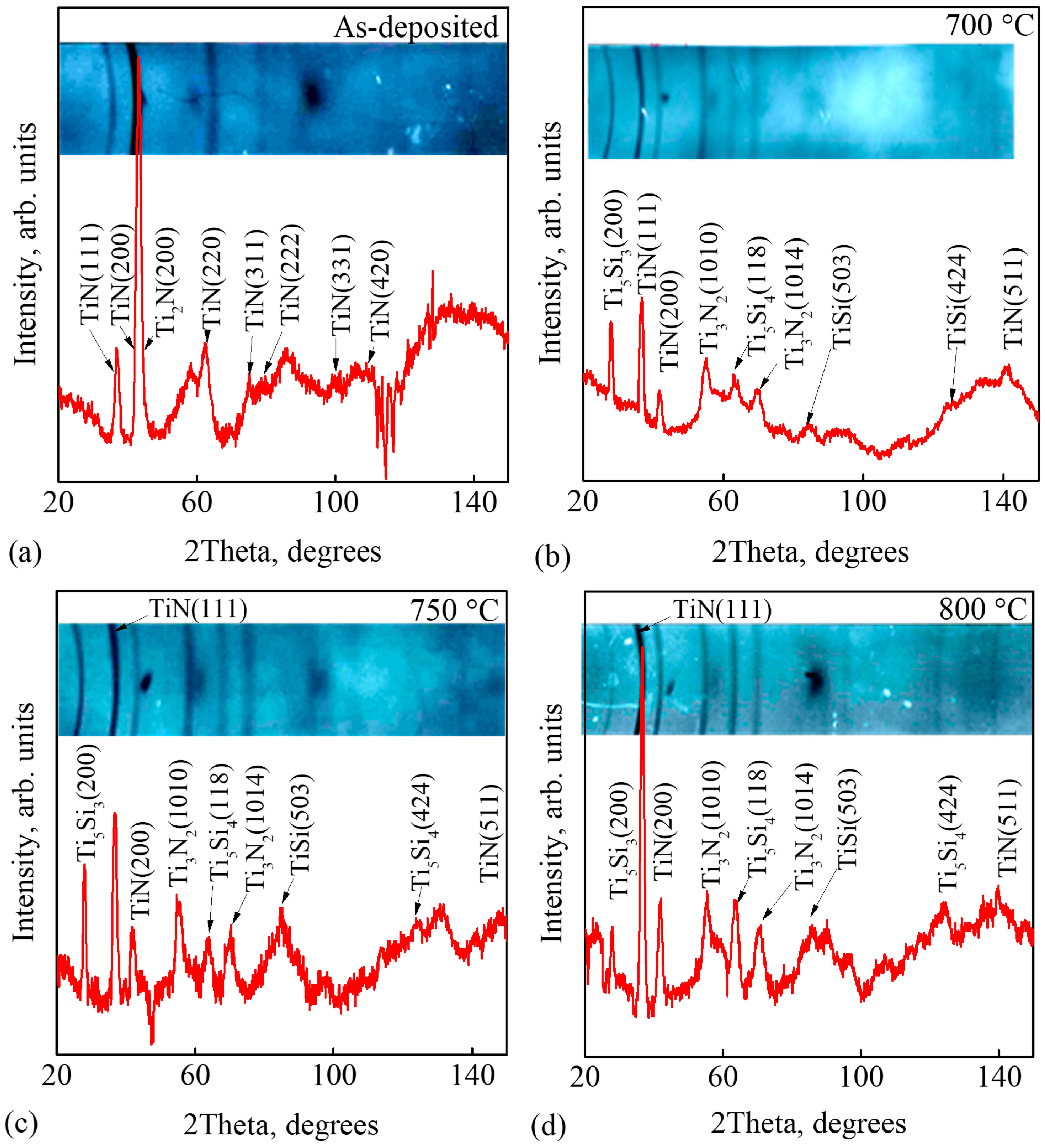
Figure S2. The XRD intensity profiles were extracted from the photographic films using a microdensitometer, and the resulting spectra are presented in
Figure 3.
Figure 3 and
Figure S3 show X-ray diffraction patterns and intensity curves of titanium nitride films on Si synthesized by magnetron sputtering (1200 W, 604 s, N
2/Ar = 30/1, 0.8 Pa, 100 °C), presented for the as-deposited state and after annealing at 700–800 °C for 30 min in Ar. For the as-deposited film in
Figure 3a, characteristic TiN reflections are observed, including TiN(111) at ~36.6°, a broad composite reflection near 42.5° from overlapping Ti
2N(200) (JCPDS 00-023-1455) and TiN(200) (JCPDS 00-038-1420) reflections, TiN(220) at ~61.8°, and weaker higher-order reflections, with the broadness of these reflections indicating a nanocrystalline structure with 4–6 nm grain size. After annealing at 700 °C (b), Ti
2N transforms to Ti
3N
2 (JCPDS 00-040-0958), evidenced by new reflections near 40°, while TiN(200) intensity decreases and TiN(111) remains strong. Additional reflections at ~38.8° and ~43.2° correspond to Ti
5Si
3(200) (JCPDS 00-029-1362) and Ti
5Si
4(118) (JCPDS 00-027-0907), marking the onset of Ti–Si interdiffusion. At 750 °C in
Figure 3c, TiN(111) becomes the dominant reflection, indicating preferred orientation, while Ti
5Si
3 and Ti
5Si
4 diffraction reflections intensify, showing continued silicide formation. Finally, at 800 °C (d), TiN(111) orientation is further enhanced, now the strongest reflection intensity in the pattern, accompanied by well-developed Ti
5Si
3 and Ti
5Si
4 phases. This progressive phase evolution highlights nitrogen redistribution and Si diffusion through TiN with increasing temperature, while no TiSi
2 phase is detected at any stage.
This analysis shows that annealing leads to noticeable shifts in the diffraction line positions, while their number increases progressively with temperature, indicating the formation and transformation of crystalline phases. Immediately after TiN film deposition, an overlap between the Ti
2N(200) and TiN(200) diffraction lines is observed, resulting in a broadened composite reflection in the 41–45° region in
Figure 3a. Such broadening is typical for closely spaced diffraction lines originating from structurally related nitride phases and suggests the simultaneous presence of both Ti
2N and TiN in the as-deposited state in
Figure S3.
After annealing at 700 °C, the nanocrystalline Ti
2N phase undergoes a phase transformation into Ti
3N
2 in
Figure 3b. This transformation is accompanied by a pronounced decrease in the TiN(200) diffraction line intensity, indicating a redistribution of nitrogen-deficient titanium nitride phases. Subsequent annealing at 750 °C and 800 °C promotes the development of the TiN phase, accompanied by the emergence of a pronounced preferred orientation along the TiN(111) plane. It should be noted that at these temperatures, mutual diffusion of Si and Ti atoms occurs within the Si–TiN system, leading to the formation of TiSi, Ti
5Si
4, and Ti
5Si
3 nanocrystals, as evidenced in
Figure 3b–d [
31,
32,
33]. However, nanocrystals of the low-resistance TiSi
2 phase (i.e., Ti
5Si
10) were not detected. This absence can be attributed to insufficient interdiffusion between Ti and Si, which is hindered by the high chemical stability of TiN nanocrystals. As a result, these nanocrystals undergo only partial decomposition during annealing at 700–800 °C for 30 min in Ar.
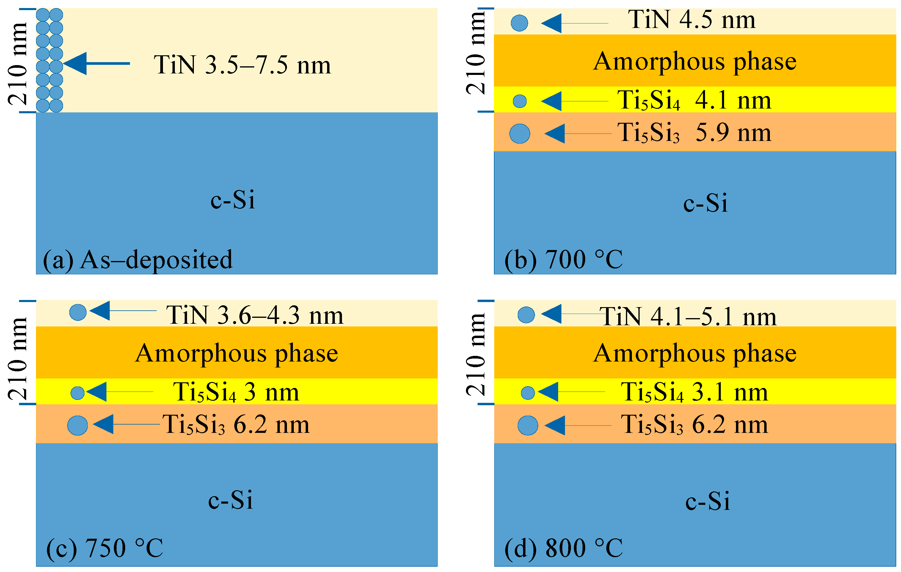
Figure 4 provides a schematic conceptual representation of the structural and compositional evolution of TiN films on Si substrates during annealing. In the as-deposited state of
Figure 4a, the film consists of a continuous ~240 nm thick TiN layer containing randomly oriented TiN 4–6 nm nanocrystals together with Ti
2N nanocrystals on the Si substrate with a sharp TiN/Si interface. After annealing at 700 °C in
Figure 4b, partial decomposition of TiN occurs with the formation of Ti
3N
2, accompanied by the emergence of interfacial Ti
5Si
3 nanocrystals near the Si interface and Ti
5Si
4 nanocrystals in regions of higher Si concentration. These crystalline phases are surrounded by an amorphous Ti–N–Si mixture resulting from nanocrystal breakdown. At 750 °C in
Figure 4c, the volume fraction of both TiN and silicide phases increases due to crystallization of the amorphous material, with Ti
5Si
3 concentrated at the Si interface and Ti
5Si
4 distributed throughout the film thickness, reflecting progressive Si diffusion. After annealing at 800 °C in
Figure 4d, the TiN layer develops a pronounced TiN(111) preferred orientation, illustrated by aligned crystallites, while surface agglomeration produces pyramidal features with voids between them. Continued growth of both silicide phases is observed, with gradual conversion of Ti
5Si
3 into Ti
5Si
4 and increased interfacial roughness. The spatial distribution of Ti
5Si
4, further from the interface compared to Ti
5Si
3, reflects the Si concentration gradient established by diffusion from the substrate. Arrows in the schematic indicate Si diffusion pathways. Overall,
Figure 4 emphasizes that phase evolution occurs through a combination of solid-state reactions, diffusion-driven redistribution, and crystallization from transient amorphous regions.
The average crystallite sizes ε and the integral intensity of the nanocrystalline phase are summarized in
Table 1. In the as-deposited state, the film contains TiN nanocrystals with average sizes of approximately 4 nm in the (111) plane and 5.8 nm in the (200) plane, along with Ti
2N nanocrystals observed in the (200) plane. An approximate evaluation of the volume of nano-TiN, calculated as the sum of intensities I
TiN(111) + I
TiN(200) + I
TiN(220), and the volume of nanosilicides, calculated as I
Ti5Si3(200) + I
Ti5Si4(118), shows that after annealing at 700 °C for 30 min in Ar, the volume of the nano-TiN phase decreases by a factor of 2 in
Table 1. This reduction is due to the decomposition of TiN nanocrystals and the formation of Ti
5Si
3(200) (~6 nm) and Ti
5Si
4(118) (~4 nm) nanocrystals, as well as the emergence of Ti
3N
2 nanocrystals and an amorphous mixture of Ti, N, and Si atoms resulting from nanocrystal breakdown.
Annealing at 750 °C leads to an increase in the volume of TiN, Ti5Si3, and Ti5Si4 nanocrystals due to crystallization of the amorphous atomic mixture and the formation of smaller nanocrystals, which may result in decreased average crystal size. After annealing at 800 °C for 30 min in Ar, both the volume of the nano-TiN phase and the crystallite sizes increase. The combined volume of Ti5Si3 and Ti5Si4 phases remains unchanged at 800 °C, but Ti5Si3 gradually transforms into Ti5Si4 due to the diffusion of Si atoms into Ti.
As a result, XRD analysis revealed that after annealing at 700 °C, 750 °C, and 800 °C, Ti
3N
2 nanocrystals formed within the TiN films alongside TiN nanocrystals. This observation is consistent with the X-ray reflectometry data, which showed a film density of 5.131 g/cm
3, corresponding to a Ti
3N
2 composition (TiN
0.66). Notably, TiSi
2 nanocrystals were not detected, which may be attributed to the high stability of TiN as a diffusion barrier [
34,
35,
36]. The strong Ti–N bonding prevents Ti atoms within TiN nanocrystals from diffusing into Si to form TiSi
2, whereas silicon atoms can still penetrate through the barrier layer at 700–800 °C, leading to the formation of TiSi, Ti
5Si
4, and Ti
5Si
3 nanocrystals. The absence of TiSi
2, in which 5 titanium atoms correspond to 10 silicon atoms, indicates insufficient silicon diffusion through the TiN layer and highlights both the effectiveness of the barrier and the inability to form a TiSi
2 layer at the Si/TiN interface below 800 °C. This behavior may also be influenced by the considerable thickness of the TiN films and the strong Ti–N bonds, which hinder mutual diffusion of Si and Ti [
37]. Therefore, it is assumed that the deposition of an intermediate Ti layer is required to form a low-resistance TiSi
2 layer at the Si/TiN interface.
3.2. Barrier Properties of TiN and SiC Films Against the Diffusion of Cu Atoms into Si
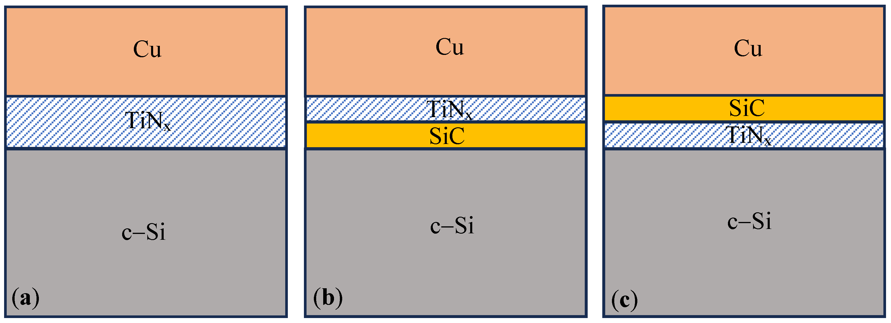
Cu provides low electrical resistance, but its high diffusivity in Si leads to Cu3Si formation during annealing, causing severe degradation of contact properties. Therefore, effective diffusion barriers are required to prevent Cu–Si interdiffusion. This subsection examines the thermal stability of Si/TiN/Cu and Si/SiC/TiN/Cu structures and evaluates the ability of TiN and SiCx nanolayers to suppress diffusion at various temperatures. In all experiments, the Cu layer thickness was approximately 300 nm. The Si/TiN/Cu structure contained a 100 nm TiN layer, whereas the Si/SiC/TiN/Cu structure incorporated 50 nm SiC and 50 nm TiN layers. The resulting structures were subjected to annealing at 500 °C, 600 °C, 700 °C, and 800 °C for 30 min.
The thermal evolution of the Cu–TiN–Si multilayer system, shown schematically in
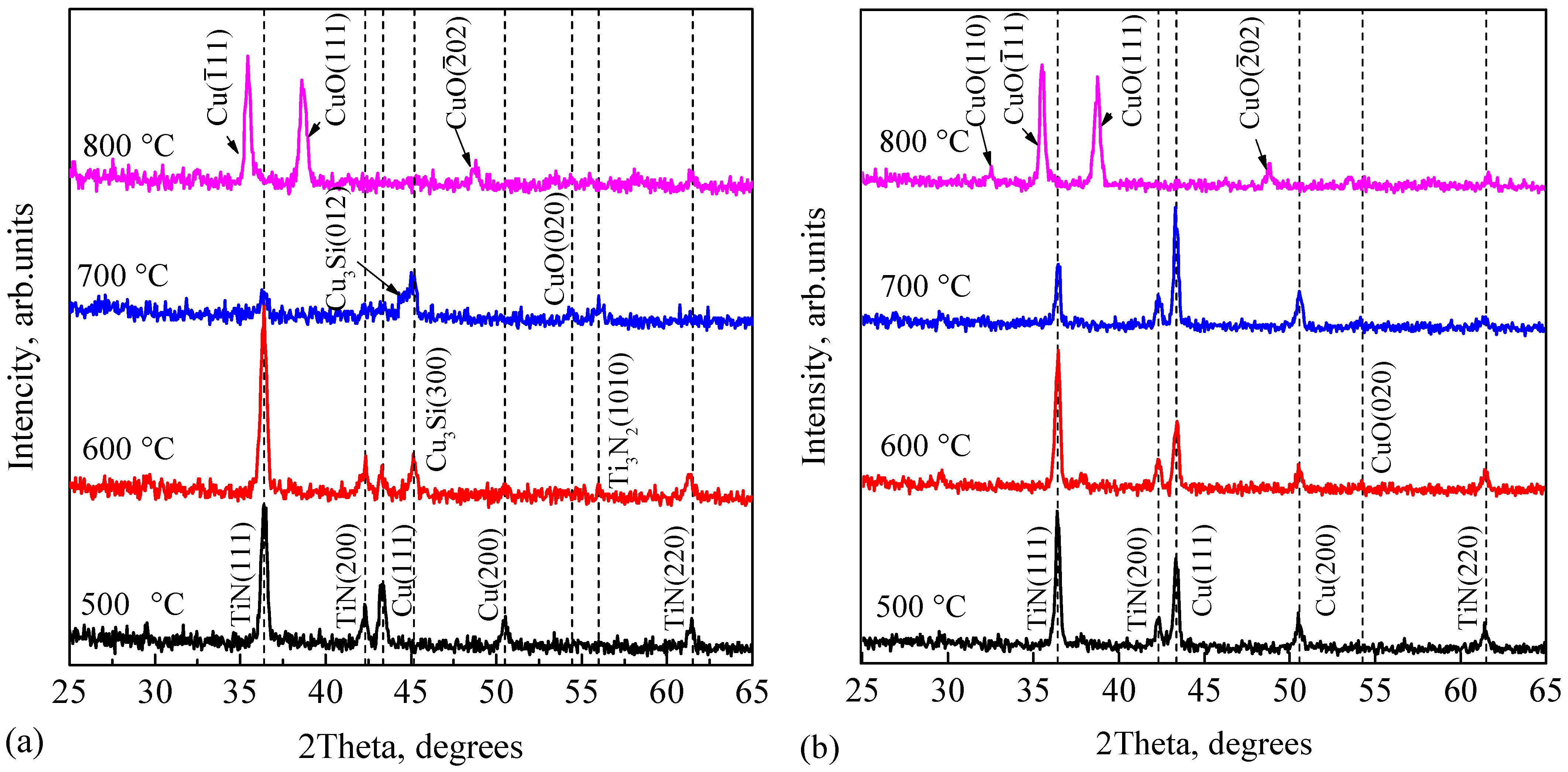
Figure 1a, was investigated by annealing at 500–800 °C for 30 min in an Ar atmosphere. Corresponding XRD data are shown in
Figure 5a. At 500 °C, XRD analysis revealed the presence of TiN(111), TiN(200), TiN(220), and Cu(111), Cu(200) phases, indicating that the TiN barrier maintained its structural integrity and the Cu layer preserved its initial crystallographic texture. Upon annealing at 600 °C, the intensity of the TiN(111) diffraction line increased, while the intensity of Cu(111) and Cu(200) diffraction lines decreased. Simultaneously, the Cu
3Si(300) phase emerged, suggesting the onset of Cu–Si interdiffusion. The increase in TiN(111) intensity is attributed to crystallite growth, whereas the decrease in Cu and other TiN diffraction lines reflects consumption of Cu in the formation of the initial Cu
3Si phase.
At 700 °C, the intensity of TiN(111) dramatically decreased, accompanied by reductions in TiN(200), TiN(220), Cu(111) and Cu(200) diffraction lines. This corresponds to partial TiN degradation and enhanced Cu–Si interaction, resulting in the formation of additional Cu
3Si phases (JCPDS 00-051-0916), namely Cu
3Si(300) and Cu
3Si(012). These observations indicate that TiN’s effectiveness as a diffusion barrier diminishes at this temperature, facilitating Cu–Si silicidation. At 800 °C, the TiN layer underwent complete structural degradation, and the Cu layer at the surface was fully oxidized due to residual oxygen. XRD patterns in
Figure 5a showed no detectable TiN or metallic Cu phases, while Cu oxide phases dominated. The absence of TiN and Cu phases indicates total decomposition of the barrier and Cu layers, with Cu oxidation replacing Cu–Si interactions.
Given the limited thermal stability of TiN observed in the Cu–TiN–Si stacks, a complementary analysis was performed on Si–SiC–TiN–Cu structures in
Figure 5b. The annealing of the Si/SiC/TiN/Cu multilayer structure at 500–800 °C for 30 min in an Ar atmosphere revealed that the thermal behavior of the system is strongly governed by the presence of the SiC interlayer in
Figure 5b. The TiN layer maintains its structural integrity at 500 °C, and the Cu layer retains its initial crystallographic texture. No significant phase transformations were observed at 600 °C, suggesting that the multilayer stack remains structurally stable at this temperature. The intensity of the Cu(200) (JCPDS 00-004-0836) phase slightly decreases, and the CuO(020) (JCPDS 00-041-0254) phase begins to appear.
At 700 °C, the intensity of the TiN(111) diffraction line decreased, whereas the Cu(111) and Cu(200) diffraction lines increased in
Figure 5b. This change is attributed to recrystallization and grain growth within the Cu layer, leading to structural reorganization rather than chemical interaction. Importantly, no Cu
3Si silicide phase was detected at this temperature. This behavior is explained by the characteristics of the SiC layer: Si atoms in SiC are strongly bonded in the rigid Si–C covalent lattice and therefore are not available to react with Cu. In addition, SiC acts as a highly effective diffusion barrier, significantly suppressing Cu–Si interdiffusion. As a result, the Cu
3Si phase, which is commonly observed around 600 °C in conventional Si/TiN/Cu systems, does not form in the presence of the SiC interlayer.
At 800 °C, degradation of the TiN barrier results in exposure of the Cu surface, which subsequently reacts with residual oxygen present in the argon atmosphere, forming copper oxide phases. Nevertheless, the Cu3Si phase remains absent even at 800 °C. The lack of Cu–Si interaction at 800 °C further confirms the exceptional thermal and chemical stability of SiC. Although the formation of Cu3Si would require the release of Si atoms from the SiC lattice, breaking the strong Si–C bonds demands significantly higher energy, making such a reaction impossible at 800 °C. Thus, even when TiN undergoes degradation, oxygen–copper reactions dominate over any potential Cu–Si interaction, preventing silicide formation.
To study the barrier properties, a three-layer Si/TiN/SiC/Cu structure, schematically shown in
Figure 1c, was also synthesized. The TiN and SiC layer sequence was changed to investigate the effects of layer arrangement on barrier characteristics. Film parameters and deposition modes remained unchanged.
For the assessment of electrical characteristics, the sheet resistance was measured using the four-point probe technique. The sheet resistance values obtained for all multilayer structures at different annealing temperatures are summarized in
Table 2. At room temperature, all samples exhibit low 0.23–0.27 Ω/sq sheet resistance, reflecting the high conductivity of the as-deposited Cu layer. After annealing at 500 °C, the Si/TiN/Cu structure shows a substantially increased 79.4 Ω/sq sheet resistance, whereas the Si/SiC/TiN/Cu and Si/TiN/SiC/Cu structures experience only minor changes (11.9 Ω/sq and 0.74 Ω/sq, respectively). This difference indicates that the presence of the SiC interlayer, regardless of its position in the stack, significantly improves the thermal stability of the metallization scheme at moderate temperatures.
The sheet resistance and thermal stability of the TiN/SiC multilayer diffusion barriers developed in this work were benchmarked against other copper barrier systems reported in the literature. The results clearly demonstrate the superior performance of the SiC-containing structures relative to conventional TiN-only barriers. The Si/TiN/Cu stack failed at 600 °C, with sheet resistance R
s rising sharply to more than 2.5 × 10
5 Ω/sq at 700 °C, confirming rapid Cu–Si interdiffusion and silicide formation. In contrast, both Si/SiC/TiN/Cu and Si/TiN/SiC/Cu stacks remained stable up to 700 °C, exhibiting remarkably low sheet resistance values of 2.3 Ω/sq and 4.9 Ω/sq, respectively. This level of stability is comparable or superior to other advanced barrier systems such as TaN and Ti/TiN bilayers, which typically fail around 650 °C with sheet resistance in the 10
3–10
4 Ω/sq range [
27]. Furthermore, the performance of the TiN/SiC multilayers approaches W/SiC composite barriers, which remain stable up to 750 °C but require more complex fabrication. These comparisons highlight that the dual-barrier mechanisms of TiN and SiC provide complementary protection. SiC effectively blocks Cu ingress due to strong Si–C bonding, while TiN maintains electrical conductivity and prevents Si outdiffusion. The ability of these multilayers to sustain low resistance at 700 °C underscores their potential for integration into Cu-based metallization schemes in advanced photovoltaic and microelectronic devices, offering a simpler and scalable alternative to more complex refractory metal systems. Similar limitations of TiN-only barriers have been reported in recent work on amorphous-like TiN films, which show significant resistance increases upon annealing above 600 °C [
14].
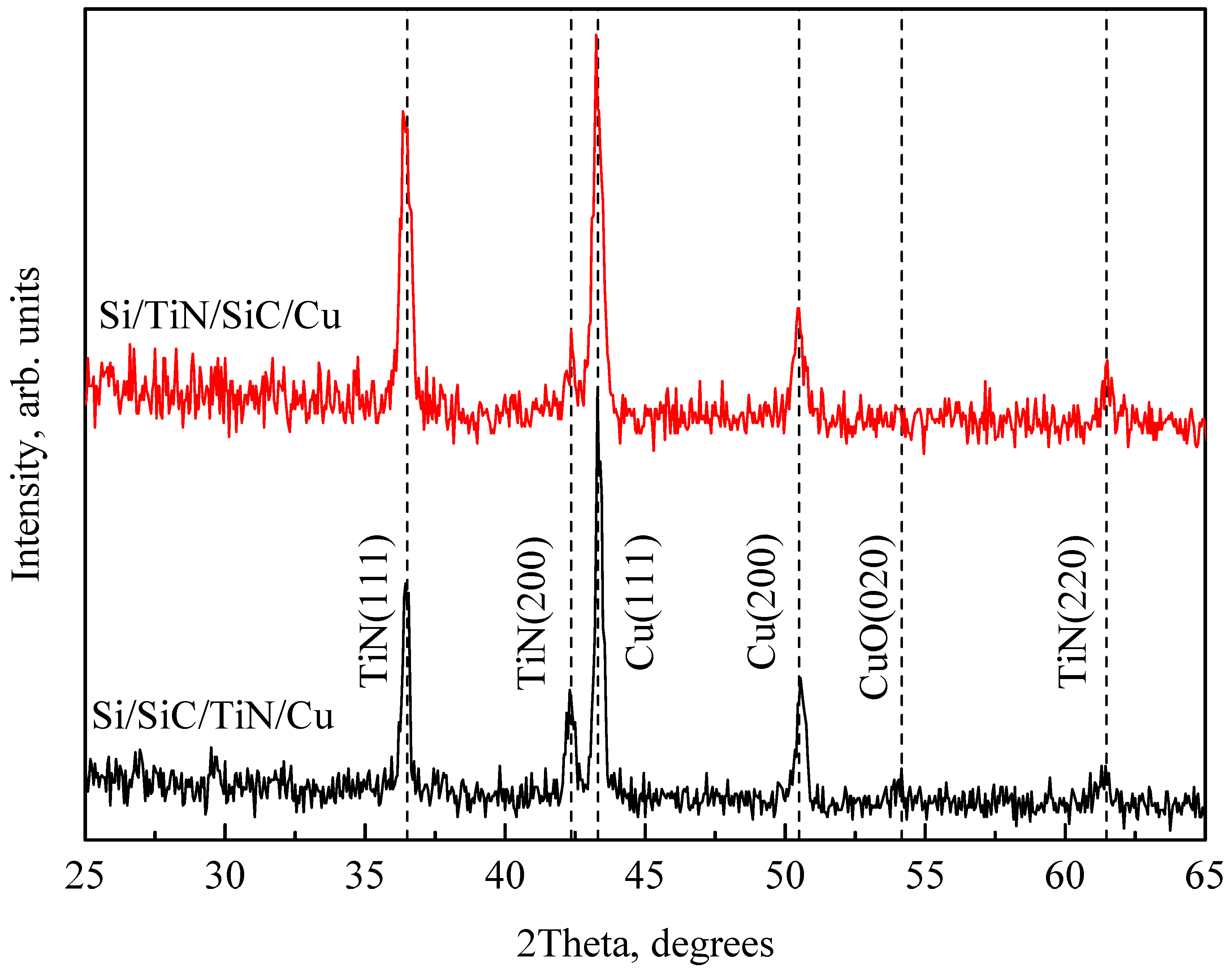
To compare the structural transformations in the Si/SiC/TiN/Cu and Si/TiN/SiC/Cu multilayer stacks, a comparative XRD analysis of both films annealed at 700 °C was performed. As seen in
Figure 6, the intensity of the TiN(111) diffraction line in the Si–SiC–TiN–Cu system annealed at 700 °C for 30 min in an argon atmosphere is noticeably lower (I
TiN(111) = 0.42, FWHM = 0.58°) compared to the Si–TiN–SiC–Cu system (I
TiN(111) = 0.71, FWHM = 0.41°). This reduction in intensity and an increase in FWHM indicate significant structural degradation. This reduction is attributed to the partial decomposition of the TiN layer caused by the active diffusion of Cu atoms into the TiN layer. Such diffusion leads to structural disordering within the TiN phase, thereby weakening its XRD signal.
The X-ray diffractograms in
Figure 6 suggest distinct differences in the structural stability of TiN depending on the multilayer configuration. The TiN(111) reflection at ~36.6° exhibits markedly different characteristics. In the Si/SiC/TiN/Cu stack, its intensity is reduced and FWHM broadens, suggesting Cu-induced structural degradation of the TiN layer. In contrast, the Si/TiN/SiC/Cu stack maintains a higher intensity and a sharper profile in terms of the FWHM, demonstrating preserved crystallinity and improved barrier performance. The TiN(200) reflection at ~42.6° follows a similar trend, further confirming the stabilizing effect of the SiC interlayer when positioned adjacent to Cu. Reflections corresponding to Cu(111) at ~43.3° and Cu(200) at ~50.4° are observed in both samples with comparable intensity, confirming similar Cu layer quality across the two configurations. Importantly, no Cu
3Si phases are detected at 700 °C in either stack, validating the effectiveness of SiC in suppressing Cu–Si interdiffusion. Minor CuO reflections appear in both cases, attributed to surface oxidation during annealing.
Overall, this comparison demonstrates that placing SiC between TiN and Cu in the Si/TiN/SiC/Cu configuration provides superior protection to the TiN barrier layer by preventing Cu penetration, thereby maintaining structural integrity and ensuring lower electrical resistance.
These results highlight the critical role of SiC as a robust high-temperature diffusion barrier and demonstrate its clear advantages over conventional TiN in Cu-based metallization schemes. Building on this understanding, future research should focus on optimizing the thickness, stoichiometry, and deposition parameters of SiC and TiNx/SiCx composite layers to further enhance barrier performance. Additionally, systematic studies employing rapid thermal annealing, long-term thermal cycling, and in situ structural diagnostics may provide deeper insight into the diffusion mechanisms and failure modes of multilayer stacks. Advanced characterization techniques such as cross-sectional transmission electron microscopy with energy-dispersive X-ray spectroscopy mapping, X-ray photoelectron spectroscopy depth profiling, and time-resolved XRD during annealing would provide valuable complementary information about the spatial distribution of elements, chemical states, and real-time phase evolution. The integration of such engineered barrier layers into full TOPCon and SHJ solar-cell architectures, combined with scalable Cu plating, represents a promising pathway toward low-cost, thermally stable, and industry-compatible metallization solutions for next-generation photovoltaic technologies.



 ,
,