
Article

Process Control by Optical Emission Spectroscopy During Reactive Magnetron Sputtering of NiVxOy Electrochromic Coatings


by
Oihane Hernandez-Rodriguez
1,*,
Gregorio Guzman
2,3,
Rocio Ortiz
1,
Ester Zuza
4,
Victor Bellido-Gonzalez
5,
Iban Quintana
1 and
Eva Gutierrez-Berasategui
1
1
Tekniker, Basque Research and Technology Alliance (BRTA), C/Iñaki Goenaga 5, 20600 Eibar, Spain
2
Polymat, Joxe Mari Korta Center—Avda. Tolosa 72, 20018 Donostia/San Sebastián, Spain
3
Department of Chemistry, Universidad Autónoma Metropolitana, Iztapalapa Campus, Mexico City 09310, Mexico
4
Department of Mining-Metallurgy Engineering and Materials Science, Polymat, Bilbao School of Engineering, University of the Basque Country (UPV/EHU), Plaza Ingeniero Torres Quevedo 1, 48013 Bilbao, Spain
5
Gencoa Ltd., 4 De Havilland Dr., Liverpool L24 8RN, UK
*
Author to whom correspondence should be addressed.
Coatings 2026, 16(2), 206; https://doi.org/10.3390/coatings16020206
Submission received: 5 January 2026 / Revised: 29 January 2026 / Accepted: 2 February 2026 / Published: 5 February 2026
(This article belongs to the Special Issue Surface Modification Techniques Utilizing Plasma and Photonic Methods)

Highlights

  • Reactive sputter deposition of NiVxOy electrochromic coatings using DC magnetron systems.
  • OES-based control enables stable monitoring in absence of monotonic voltage response.
  • Identification of key plasma transition points along hysteresis using OES signals.
  • Microstructural and electrochemical performance linked to pressure and PEM control.
  • OES-control process enables scalable fabrication of EC NiVxOy layers.

Abstract

This paper presents a study on the development and optimisation of thin films of nickel-vanadium oxide (NiVxOy) deposited by DC reactive magnetron sputtering (RMS) controlled by P.E.M. (plasma emission monitoring). The hysteresis behaviour of the Ni emission signal as a function of oxygen incorporation was analysed using optical emission spectroscopy (OES), enabling the identification of critical working points along the hysteresis loop and their correlation with film growth mechanisms. Compared to the non-monotonic nature of the target discharge voltage signal, OES provided a simplified response for real-time process control. A set of coatings was deposited under various working pressures (0.6 and 2.0 Pa) and plasma emission monitoring (P.E.M.) conditions and was thoroughly characterised in terms of microstructure, composition, optical modulation, and electrochemical performance. Films deposited at high pressure and under 30% P.E.M. conditions showed an optimal balance between optical modulation (21%) and charge density (4 mC/cm2), which was attributed to the increased Ni3+ content and the surface cracks at low density.

1. Introduction

Electrochromic devices (ECDs) are a crucial energy-saving technology with a high potential in various applications, particularly in window glazing for buildings, vehicles, and aircraft [1,2,3,4,5,6,7,8,9,10,11,12,13,14,15]. Smart windows in particular offer energy-saving, safety, comfort, and additional functionality benefits. Recently, there has been a lot of interest in electrochromic (EC) materials, such as transition metal oxides (TMO), due to their ability to reversibly change between transparent and dark colouration via the reduction-oxidation reaction when charging or discharging the device by applying an electric field. In addition, TMOs show low power consumption (i.e., less electrical energy required to induce the optical transition), high colouration efficiency (CE), and memory effect under open circuit conditions [16,17]. Nickel oxide (NiO) is widely used as an anodic layer in ECDs due to its ability to change colour reversibly after oxidation, a property known as anodic colouring. Passerini et al. [18] suggest that in the presence of non-aqueous electrolytes containing lithium, the first insertion of the ions into the nickel oxide lattice causes an irreversible modification of its structure. This promotes a volume change that creates sufficient space within the porous structure for the subsequent reversible movement of lithium ions, as illustrated below:
Activation step:
N i O x + y L i + + y e L i y N i O x
Reversible reaction step:
L i y N i O x   c o l o u r i n g b l e a c h i n g   L i y z N i O x + z L i + + z e
This makes it a suitable complement to tungsten oxide (WO3), which functions as the cathodic layer. Together, they enable high optical contrast and efficient device operation. NiO also offers high cycling stability and good transparency in its reduced state [19,20,21]. However, its performance is limited by several factors, such as a narrower optical modulation range, lower transparency in the bleached state compared to WO3, and lower charge densities in thin films [22]. These limitations can lead to charge imbalance within the system; therefore, it is necessary to optimise NiO coatings to achieve higher charge densities and avoid restricting the overall efficiency of the ECD [23].
NiO thin films are deposited by different chemical and physical methods, such as spray pyrolysis [24,25], e-beam deposition [26,27,28], electrodeposition [29,30], sol–gel [31,32,33] or magnetron sputtering (MS) [22,33,34]. The electrochromic performance of NiO films strongly depends on the electrolyte used: typical values of coloration efficiency (η) and optical modulation (ΔT) of NiO thin films are between 37.63 and 33.59 cm2/C and 40.6% to 57.19% [22,33], respectively, for non-aqueous LiClO4 electrolyte, and 42.18 to 14.86 cm2/C and 80.8% to 75.34% for KOH electrolyte [34,35]. While Li+ in non-aqueous media provides greater durability and stability with a lower electrochromic response, H+ in aqueous KOH accelerates the switching response but causes greater chemical reactivity and film degradation.
Reactive magnetron sputtering (RMS) is a versatile industrial method for large-area thin film deposition, with no harmful gas or liquid emissions. When evaluated through lifecycle environmental assessment (LCA) using the ReCiPe methodology, RMS-based PVD coatings show lower environmental impacts than conventional wet technologies, particularly in terms of damage to human health, ecosystems, and resource availability [36,37]. However, the ferromagnetic material, such as pure nickel (Ni), due to the high magnetic permeability, shunts part of the magnetic flux, modifying the original magnetic field distribution above the target. This interaction between the ferromagnetic target and the magnetron field can cause unwanted effects, such as distortion of the magnetic field and reduction in the plasma confinement and ion density, which are critical for efficient sputtering and uniform film growth. Furthermore, as the ferromagnetic target erodes, the changes in the resulting magnetic field would be magnified. In order to avoid this, a high-strength magnetic field magnetron must be used, or the Ni target geometry must be modified, requiring both strategies a high-cost investment. A more economical alternative would be the de-ferromagnetization of the Ni target material with the implementation of a non-magnetic material, such as vanadium (V). Ni-V is a commonly available non-magnetic alloy with a limited number of publications discussing its electrochromic properties [38,39]. In addition, although vanadium doping has been shown to decrease the bleached-state transmittance compared to pure NiO due to the formation of acceptor states and enhanced p-type conductivity, Ni-V oxide films exhibit a significantly enhanced charge capacity, which is a key requirement for anodic electrochromic layers. Previous studies reported a maximum colouration efficiency of 63.8 cm2/C with 52% of optical modulation for a coating thickness of 321 nm using a 1 M LiClO4-PC electrolyte. Other dopants such as Mg, Al, Si, Zr, Nb, or Ta have been reported to maintain or even enhance the bleached-state transmittance of NiO films. However, they result in a reduced reversible charge density compared with vanadium containing formulations. Alternative doped system, include Ni-W oxides, which present a higher charge density at the laboratory scale compared with Ni-V. In practice, Ni-W targets are constrained by tungsten’s low sputtering yield and high cost and composition drift resulting from preferential sputtering during target erosion, limiting their industrial stability. Therefore, despite its optical compensation in the bleached state, NiVxOy appears to be a more suitable candidate for industrialisation. In this context, the critical factor for achieving good electrochromic performance would be to optimise the oxygen injection during sputtering, as demonstrated by A. Niklasson et al. for aqueous electrolytes [40] and Ye J. et al. for organic electrolytes [38].
Among the control strategies reported for reactive magnetron sputtering, only studies correlating oxygen flow with target discharge voltage have been published to date [41,42,43]. These works analyse the discharge voltage response under varying gas flow conditions, but do not implement active feedback control systems. Existing approaches rely exclusively on constant oxygen flow configurations without implementing dynamic regulation of the reactive gas based on real-time discharge voltage signals [34,38,39,44]. This limited use may be attributed to the fact that this discharge voltage-based control is not always the most suitable approach, as its effectiveness can vary depending on the material system: in some cases, the relationship between the target discharge voltage and the reactive gas is non-monotonic, which complicates the feedback control and limits the process stability [45,46]. A recent study has developed a control system to eliminate the issue of monotonic signals in the RMS process [47]. The method is based on real-time analysis of the correlation between target discharge voltage and the plasma emission monitoring (P.E.M.) optical signal, but its implementation requires a high level of technical knowledge and a complex control [47]. However, the authors state that the process could be controlled by optical emission spectroscopy (OES), relying exclusively on the P.E.M. signal. This approach constitutes a predictable control methodology compared to the conventionally applied discharge voltage-based technique. The improved sensitivity of this technique was demonstrated in earlier work on WO3 [48], where up to a 20% variation in tungsten emission was detected between the oxide and poisoned states, while the target discharge voltage only revealed a 1% difference. In that study, OES was used to identify just the oxidation point in order to increase the deposition rate without compromising optical transmittance.
Here, OES control will be employed to search for the optimal oxygen level for the deposition of NiV oxide (NiVxOy) coatings. The relationship of the industrial P.E.M. sensor (evaluated at three different points and at two working pressures) with coating properties, such as microstructure, composition, charge density and optical and electrochromic behaviour, will be analysed to find the optimal sensor working area.

2. Materials and Methods

2.1. Thin Film Deposition

The NiVxOy thin films were deposited by RMS using a 3-inch target diameter balanced magnetron cathode and a NiV target (92 at% Ni/8 at% V, 99.95% purity) on ITO-coated glass substrates (2.5 × 2.5 cm2) with a sheet resistance of 12 Ω/sq. The substrates were ultrasonically cleaned in ethanol for 15 min and placed at 20 cm from the target surface. The chamber was evacuated to a base pressure of 1 × 10⁻⁴ Pa. The target was cleaned by pre-sputtering in Ar atmosphere (139 sccm, 99.99% purity) for 10 min before every deposition. The power density was fixed at 2.2 W/cm2 (corresponding to 100 W) and applied to the NiV target by an Advanced Energy DC Pinnacle Plus power source (Advanced Energy, Denver, CO, USA). The thickness of the deposited NiVxOy thin films was kept constant at a value of 150 ± 10 nm. The chamber pressure and oxygen flow (99.99% purity) were varied to study the correlation between these process parameters and the coating properties and optimise the electrochemical behaviour of the deposited NiVxOy thin films. The O2 reactive gas flow was controlled through a mass flow controller (MFC) regulated by an advanced reactive feedback control system (Speedflo, Gencoa, Liverpool, UK), an industrial tool which provides optimum controller parameters for the reactive sputtering process based on Pseudo- Derivative Feedback (PDF) control with parameters Kp = 2, Ki = 0.01, and Kd = 0 [49]. The Speedflo controller has integrated an Ocean Optics SD2000 spectrometer, which quantified the emission over the range of 200–850 nm with a resolution of 1 nm to analyse and control the plasma created during the deposition process at subsequently selected values.
P.E.M. (%) of the nickel OES line at 352.3 ± 0.5 nm refers to the relative intensity of a selected optical emission line, normalised to its maximum value (see Supplementary Information Figure S1). This line was chosen because it corresponds to the most intense peak in the optical emission spectrum of nickel. During the RMS process, both the P.E.M. signal and the target discharge voltage were simultaneously monitored to evaluate the plasma behaviour under varying O2 flow conditions. The O2 flow was varied while maintaining a constant Ar flow of 139 sccm (standard cubic centimetres per minute). Two different pumping speed scenarios were considered: 398 L/s and 115 L/s, corresponding, respectively, to a low-pressure vacuum of 0.6 Pa, typical of MS processes (LP) and a high-pressure vacuum of 2.0 Pa, commonly employed in the synthesis of electrochromic NiO [34,50] or NiVxOy coatings [38] (HP). The P.E.M. signal was selected as the control variable because its behaviour remains similar for different target materials and directly reflects changes in the target surface state, which facilitates the definition of operating regimes compared to the target voltage. The P.E.M. signal was processed to identify the inflexion point occurring during the O2 flow ramp. The measured signal was first denoised using a cubic smoothing spline, which provides a smooth and differentiable representation while suppressing high-frequency noise. Once the spline was fitted, the time derivative was obtained analytically by differentiating the piecewise-polynomial representation of the spline. This avoids finite-difference noise amplification and removes the need for derivative windowing. As a result, the spline smoothing factor is the only numerical parameter used in the procedure, which in this work was fixed to a value of 150. The inflexion point was then defined as the minimum of the first derivative of the P.E.M. signal in the time domain.

2.2. Characterisation Methods

The morphology of the deposited NiVxOy films was visualised using a high-resolution FE-SEM Ultra Plus Zeiss equipment (Carl Zeiss Microscopy GmbH, Jena, Germany) for scanning electron microscopy (SEM). The coating thickness was measured by a surface profiler (Dektak8, Veeco Instruments Inc., Plainview, NY, USA) and by SEM on silicon pieces used as process witnesses. The film thickness was maintained at 150 nm by pre-calibrating the deposition rate, adjusting the deposition time accordingly, and verifying the thickness by profilometry and SEM. The structural properties of the NiVxOy thin films deposited on ITO-coated glass samples were analysed using a 31D8 Advance Bruker X-ray diffractometer (Bruker AXS GmbH, Karlsruhe, Germany), with Cu Kα radiation (λ = 1.5406 Å) in Bragg–Brentano θ–2θ geometry, a step size of 0.02° and a step time of 7.2 s. A Thermo Scientific ESCALAB 250Xi system (Waltham, MA, USA) was used for X-ray photoelectron spectroscopy (XPS) measurements, employing monochromatic Al Kα radiation (1486.68 eV) operated at 220 W and 14.6 kV with a 650 μm spot size. Survey spectra were collected at a pass energy of 100 eV, while high-resolution spectra for individual elements were acquired at 40 eV, with an energy step of 0.1 eV. Peak fitting was performed using Thermo Avantage data processing software, applying Shirley-type background subtraction and mixed Gaussian-Lorentzian peak shapes (default in Avantage). No truncation of peaks was applied; the full peak envelopes and tails were included in the fitting to ensure accurate representation of Lorentzian contributions. The full-width at half maximum (FWHM) values were constrained within a fixed range of 0.5–3.5 eV to maintain physically consistent peak shapes. These constraints prevent unrealistic broadening and are consistent with instrumental resolution and chemical state variations. All binding energies were calibrated with respect to the adventitious carbon C 1s peak at 284.8 eV. Quantification was carried out using sensitivity factors provided by the Avantage library, assuming a homogeneous composition within the probed volume (~10 nm depth). It should be noted that XPS is a surface-sensitive technique. Therefore, the reported atomic percentages represent near-surface composition and should not be directly interpreted as bulk stoichiometry.
The transmittance spectra of coated glass substrates were measured using a Perkin Elmer Lambda UV/VIS/NIR spectrophotometer (Perkin Elmer, Waltham, MA, USA). The average visible transmittance (AVT) was calculated according to the EN 410:2011 standard.
Electrochemical measurements were performed in a three-electrode cell using a 1 M LiClO4 solution in propylene carbonate as the electrolyte. The working electrode was a NiVxOy layer deposited on an ITO glass substrate with an area of 1.2 cm2. The counter electrode was a Pt wire, and the reference electrode was Ag/AgCl placed inside a Luggin capillary to avoid possible contamination of the system. Cyclic voltammetry (CV) was conducted over a discharge voltage range of −1 V to +1 V, using different scan rates ranging from 5 to 250 mV s−1. The ion diffusion coefficient (D, cm2/s) can be calculated using the Randles-Sevcik equation (Equation (3)) applied to the CV measurement results [17]:
i p = 2.69 · 10 5 n 3 / 2 A C ( D · v ) 1 / 2
where ip is the peak current (A), n is the number of electrons involved in the electrochemical reaction (in this work n = 1, corresponding to the Ni2+/Ni3+ redox process), representing the stoichiometric electron exchange per molecule, A is the treated electrode area (cm2), C is the concentration of Li+ (mol/cm3), and v is the scan rate (V/s). The diffusion coefficient derived from the Randles–Sevcik relation is interpreted as an apparent kinetic parameter. Since the charge storage in these films is predominantly pseudocapacitive, the assumptions of semi-infinite linear diffusion are not strictly fulfilled. Therefore, the calculated D values are used exclusively for relative comparison between samples and should not be regarded as absolute ion transport coefficients.
Chronoamperometry (CA) measurements were employed to evaluate the Li-ion intercalation/deintercalation process as a function of time, with measurements taken at −1 V and +1 V for 15 s at a time, for a total period of 4000 s. The response time was defined as the time required for the charge associated with the ion insertion/extraction process to reach 63% of the total charge exchanged during a complete insertion/extraction cycle.
The transmittance at 550 nm was simultaneously measured during the electrochemical measurements using a spectrophotometer (EPP2000C-25um Slit UV-Vis StellarNet, Tampa, FL, USA). The optical modulation, which is an important parameter for EC materials, is defined by Equation (4):
ΔT = Tb − Tc
where Tb and Tc are the transmittance of the bleached and coloured states. The optical density (ΔOD) per unit of inserted charge density (Q) and colouration efficiency (η) values of the coatings were calculated using the following equations [34]:
Δ O D = l o g T b T c
η = Δ O D Q

3. Results

3.1. Analysis of the Hysteresis Behaviour of Reactive NiVxOy Thin Film Deposition

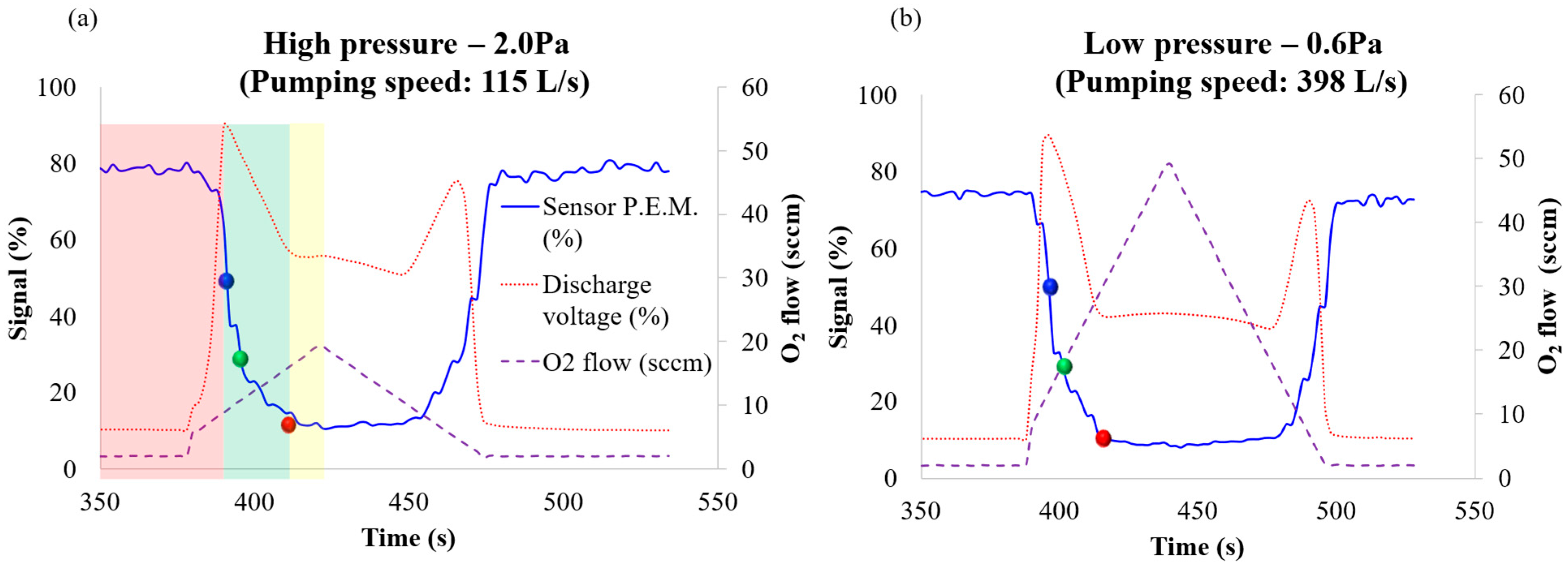
Figure 1 shows the hysteresis curves corresponding to the two different process pressures considered in the study (LP and HP).
Typically, the evolution of the reactive magnetron sputtering process is described by three distinct regions (highlighted in Figure 1), which are determined by the amount of reactive gas interacting with the target surface and explained in our previous work [48]: the metallic region (red area), the oxidised region (green area), and the poisoned region (yellow area). The discharge voltage curves exhibited a non-monotonic behaviour under varying oxygen flow, which complicates its use for feedback control as the discharge voltage shows changes in the sign of the process gain (first derivative). This complexity has been reported in the literature for RMS processes [46,51,52]. In contrast, the P.E.M. signal shows a simple and monotonic decreasing curve in function of O2 flux, making it a simpler and more user-friendly method for controlling the deposition process of this type of material. As illustrated in Figure 1a,b and Table 1, the pumping speed significantly influenced the oxygen flow required to oxidise the target surface.
At high pressure, lower O2 flow rates were necessary to reach similar oxidation states within the same time frame compared to low-pressure conditions. This is attributed to the variation in the “partial pressure/residence time” of O2 due to differences in pumping speed at different pressures. At lower pressures (higher pumping speed), more O2 is evacuated for the same flow rate, reducing the O2 flux to the target. For a given O2 flow, a higher pumping speed results in a lower partial pressure and a shorter residence time of O2 in the vacuum chamber and on the target surface. Therefore, to achieve target poisoning, a higher O2 flow would be required to maintain the same O2 partial pressure. As a result, under identical O2 flows, the Ni signal curve shifted more abruptly at higher pressure, potentially complicating the identification and calculation of stable operating points for process control. For this reason, hysteresis curves under HP conditions were carried out using an O2 flow of 20 sccm, instead of the 50 sccm used under LP conditions, in order to avoid an excessively fast transition of the target to the poisoned state.
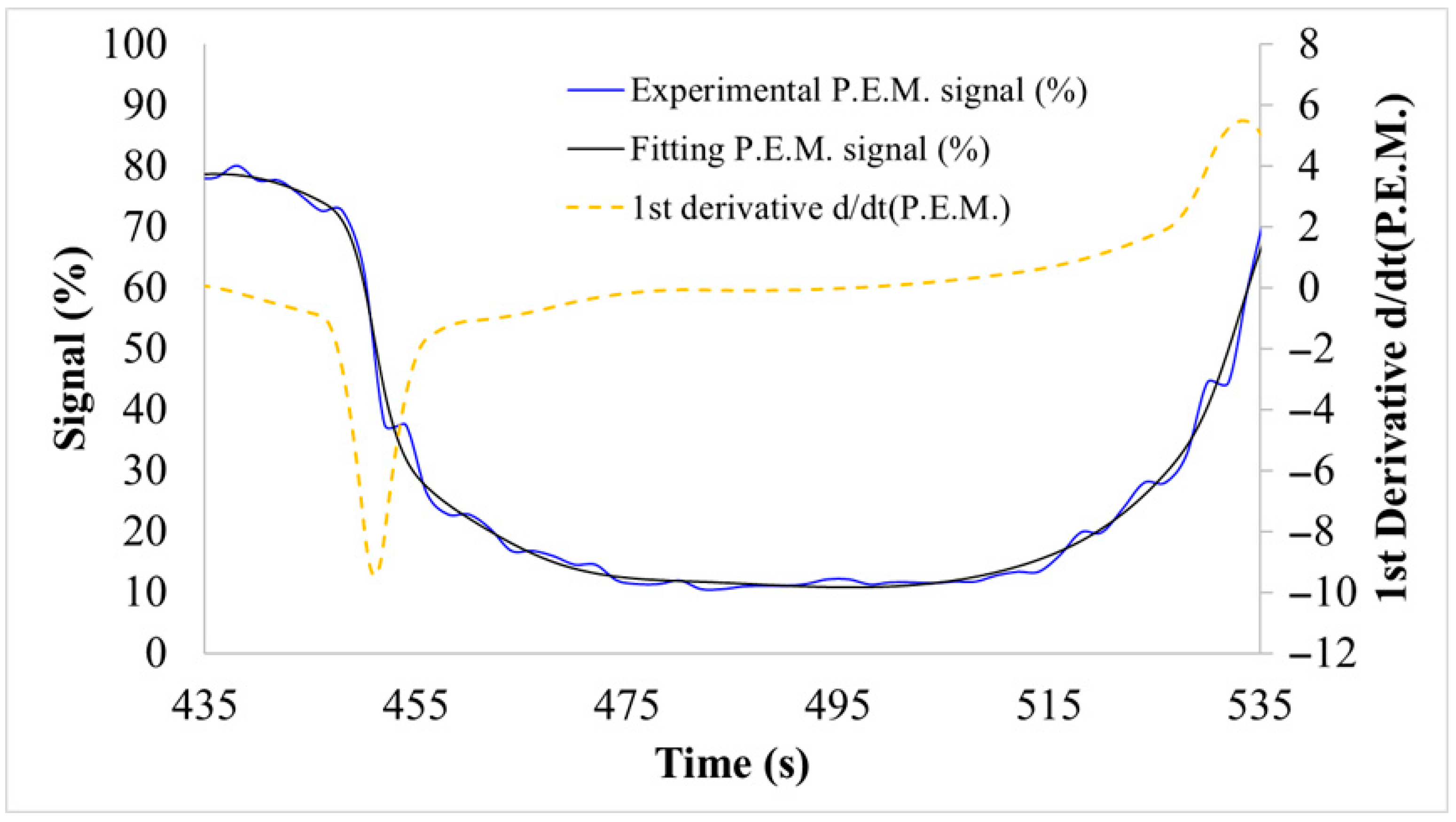
In order to establish a correlation between the target oxidation state and the deposited NiV thin film electrochemical properties, three different coatings for each pressure scenario (LP and HP) were deposited considering the three different oxidised states identified for the P.E.M. signal in the Hysteresis curves (Table 1): inflexion (blue dot in Figure 1), oxidised (green dot in Figure 1) and poisoned (red dot in Figure 1). The methodology employed to select these points in the Hysteresis curves follows a mathematical analysis where the inflexion point, defined as the minimum of the derivative (d/dt (P.E.M.)) [48,53], represents the highest dynamic consumption rate of reactive gas and provides kinetic insight into the process (Figure 2) [54,55,56]. The poisoned point, corresponding to the minimum reactive gas consumption rate, indicates full coverage of the NiV target by NiVxOy. And the oxidised point is an arbitrary value between the maximum and minimum consumption, which was determined by calculating the average value between the inflexion point and the poisoned point.
The deposition rate was found to be influenced by the selected point along the Hysteresis curve and the working pressure (see Table 1 and Figure S2). This behaviour can be explained by the Reactive Magnetron Sputtering models by Berg [57] and Depla [58], which show that the deposition rate increases when the target is less poisoned, due to the higher sputter yield of the metallic state compared to the compound, corresponding in our case to a higher Ni P.E.M. signal (%). Figure S2 illustrates the correlation between the selected Ni P.E.M. signal (%) point, the working pressure and the resulting deposition times, confirming that the process conditions remained stable during deposition. Moreover, under our experimental conditions, lower working pressure improves deposition efficiency, probably due to a reduction in the number of collisions between sputtered atoms and gas molecules in the plasma, which enhances the transport of sputtered atoms to the substrate [58]. This is supported by the observed decrease in deposition time under low-pressure conditions.

3.2. Effect of the Pressure and Ni P.E.M. % Point on the Structural and Optical Properties of the Coatings

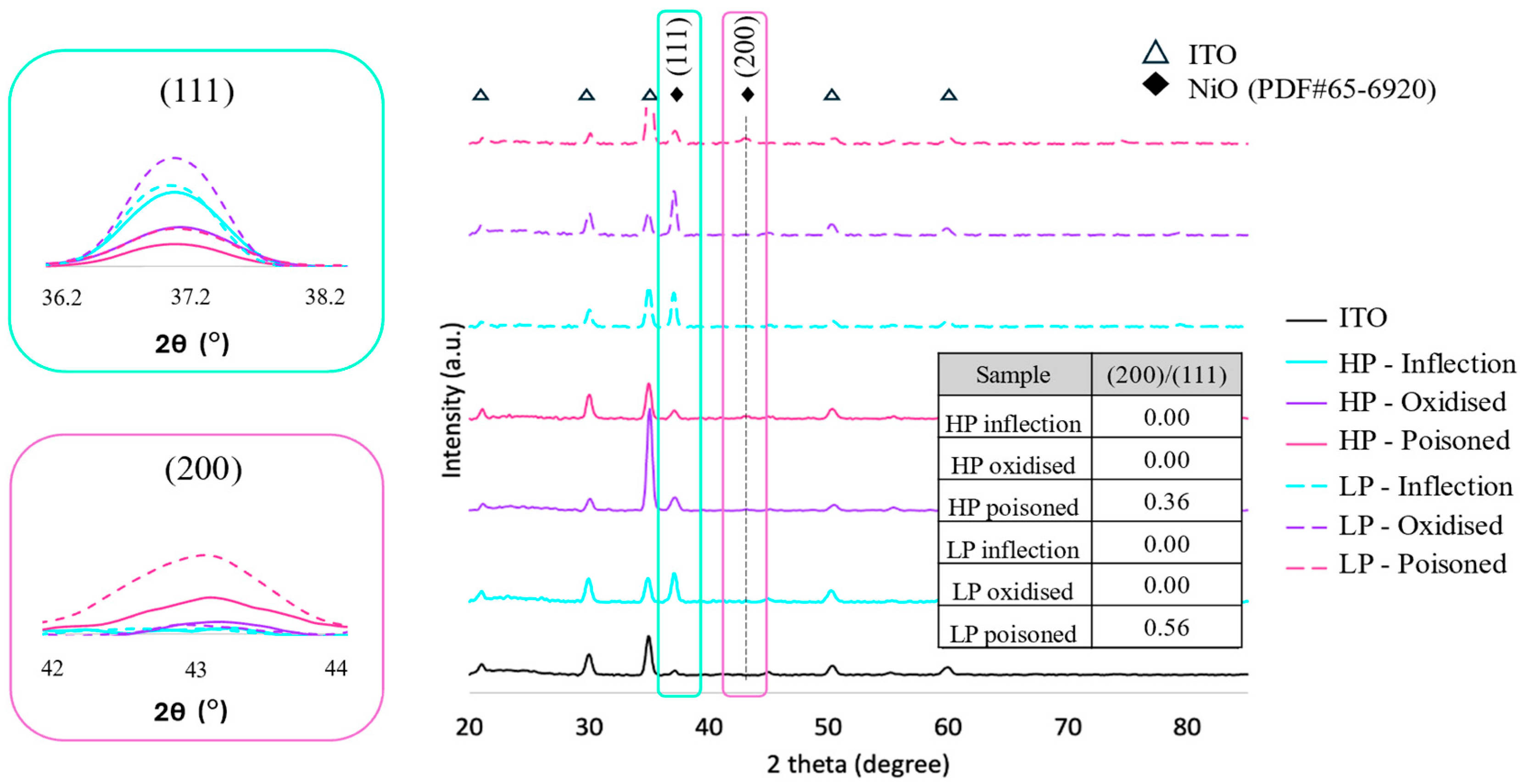
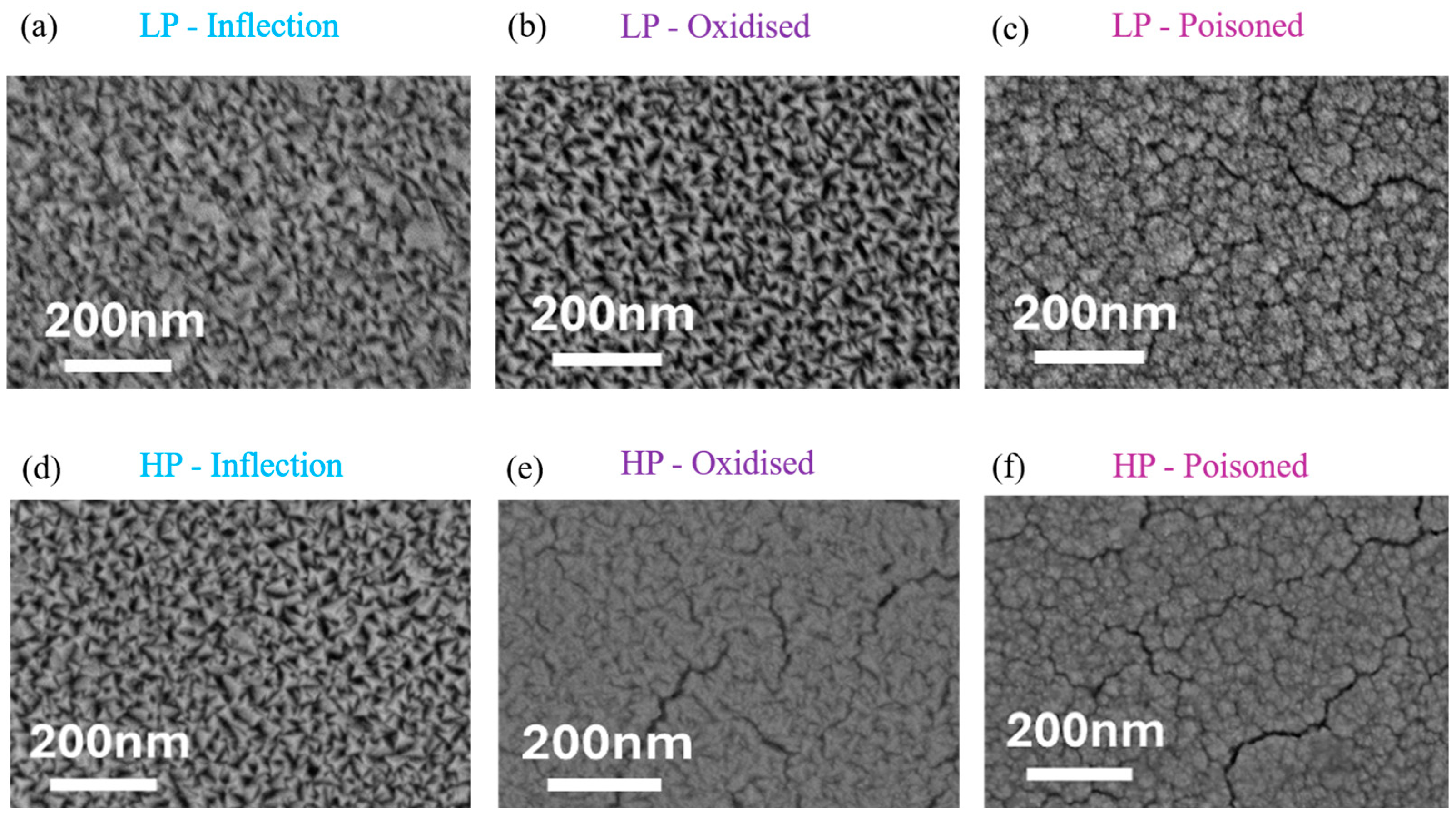
In order to analyse the influence of the sputtering process parameters (process pressure and oxidation state) on the composition of the deposited NiVxOy coatings, XRD analysis were done on all the coated samples, resulting in the observation of two NiO diffraction peaks at 2Ꝋ 37.1° and 42.8° which corresponds to the (111) and (200) planes of NiO (Figure 3). No peaks from vanadium or vanadium oxide appeared in the XRD patterns of the NiVxOy films, indicating that vanadium might exist as an amorphous phase or incorporated substitutionally into the film structure [59]. The most intense reflection in each case was determined to be (111), which is in line with a cubic crystal structure in the Fm-3 m space group. The total area under the diffraction peak in the (111) direction of NiO films slightly decreased with increasing O2 concentration. This trend, along with the appearance of the (200) peak under poisoned conditions, suggests a change in the growth morphology. Specifically, higher oxygen content during deposition may promote a transition from columnar growth to more granular, cauliflower-like surface as evidenced by the SEM images (Figure 4b,f). The appearance of the (200) plane peak indicates the coexistence of multiple orientations, although a complete texture analysis would require pole figure measurements. These qualitative observations reveal a direct correlation between excessive O2 levels, coinciding with a marked decrease in Ni P.E.M. (%) and a reduction in discharge voltage (in Figure 1 and Table 1) [30,39]. No diffraction peaks corresponding to vanadium or vanadium oxides were observed in the XRD patterns of the NiVxOy films, suggesting that vanadium does not form separate crystalline phases. Instead, it appears to be incorporated substitutionally into the NiO lattice. The slight peak shifts from the reference card further support this interpretation, previously reported by A. Kotta et al. [60], as vanadium and nickel possess similar atomic masses and ionic radius, allowing vanadium atoms to replace Ni atoms with minimal lattice distortion (from 4.19 to 4.18 Å). Crystallite sizes were estimated from the Debye-Scherrer formula [61]:
D = 0.9 λ β c o s θ
where λ is the wavelength of the X-rays (Cu Kα λ = 1.54056 Å), β is the full width at half maximum (or FWHM) of the diffraction spectra, and θ is the Bragg angle relative to the plane surface. The analysis was performed using the diffraction peak at 37°. The calculated crystallite sizes were 20.1 nm, 21.3 nm and 14.1 nm for the LP–inflexion, LP–oxidised and LP–poisoned conditions, respectively, and 17.5 nm, 13.7 nm and 15.7 nm for the HP–inflexion, HP–oxidised and HP–poisoned conditions. Small crystallite size was observed in the NiVxOy film at the HP-oxidised point.
SEM surface images of the NiVxOy coated samples (shown in Figure 4) also revealed a relationship between oxygen (or Ni percentage) and thin film structure, showing tetrahedral morphologies for layers grown in the inflexion and oxidised states and a cauliflower-like microstructure for layers grown in the poisoned state. This morphological change is consistent with the crystal state observed in Figure 3 and can be caused by the different kinetic energy of the atoms at each oxidation state and by having the inflexion and oxide points with higher target discharge voltage levels than the poisoned point (Table 1), leading to a higher energy bombardment. Similar results have been observed by H. Lin et al. [41] and Y. Tang et al. [33], where the surface microstructure of NiO thin films was found to correlate with both the energy or target discharge voltage levels and the O2 flow under different reactive sputtering conditions, producing cauliflower-like microstructures under O2 deficit or excess and tetrahedral microstructures at the oxidised point. In addition, coated samples developed at high pressures and oxidised and poisoned P.E.M. points showed superficial cracks (Figure 4e,f). These microstructures have been previously observed by Haonan Li et al. [22] when preparing NiO thin films by DC magnetron sputtering at different process pressures, finding that NiO coatings with a small concentration of surface cracks showed better electrochromic performance.
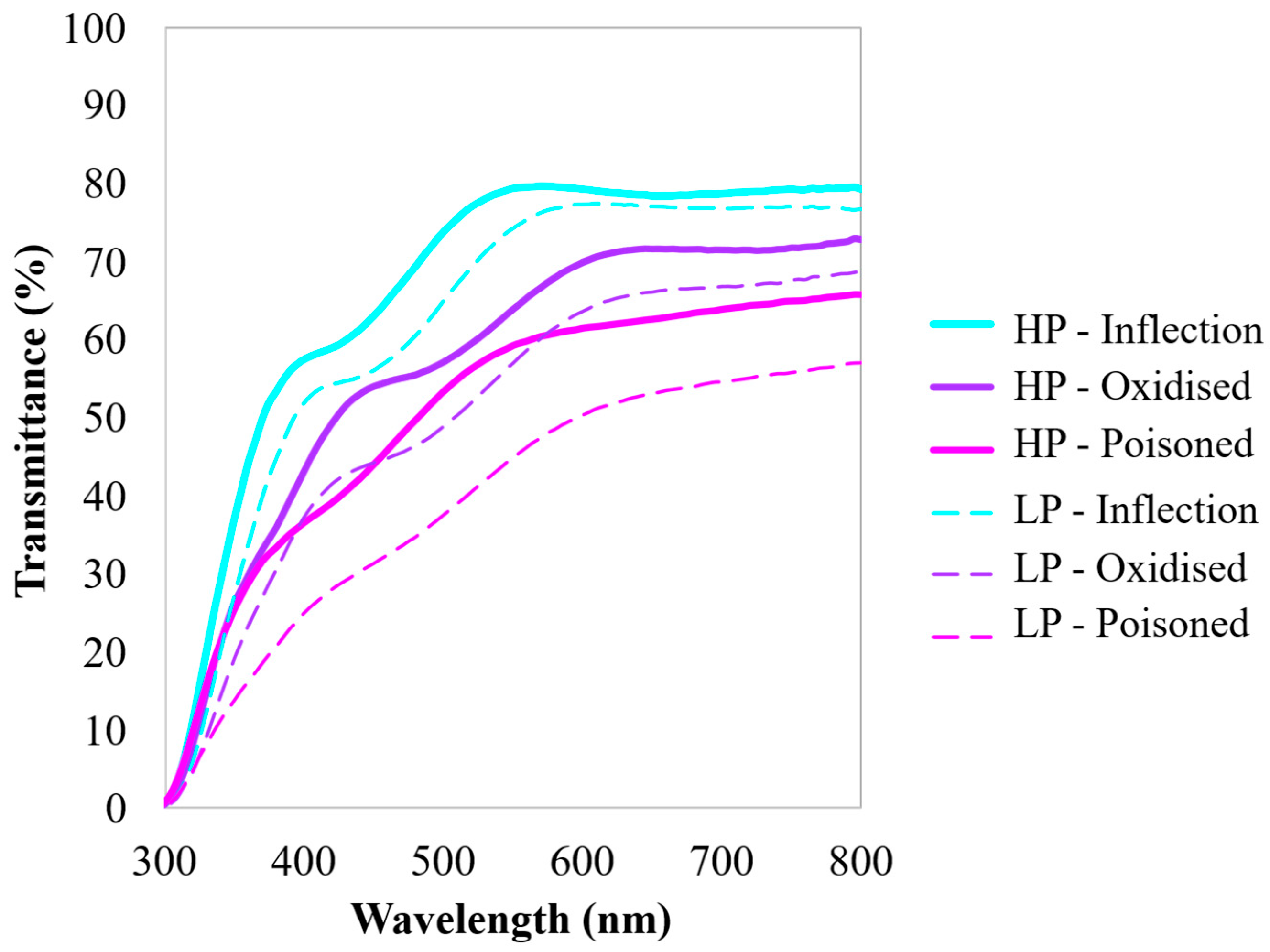
Besides phase composition and surface microstructure, the effect of O2 flow also influenced the optical properties of the coatings. As shown in Figure 5, the optical transmittance of all deposited NiVxOy thin films in the visible wavelength range decreased with the reduction in Ni P.E.M. signal, due to the increase in oxygen content, which introduces oxygen interstitial defects in the coating, increasing the scattering between light and atoms, and reducing the transmittance. This phenomenon is consistent with findings reported by several researchers [62,63,64], in contrast to conventional oxides such as WO3 [48], where increasing the oxygen content leads to higher transmittance of the coating.

3.3. Effect of the Pressure and Ni P.E.M.% on the Electrochemical and Electrochromic Performance of NiVxOy Thin Films

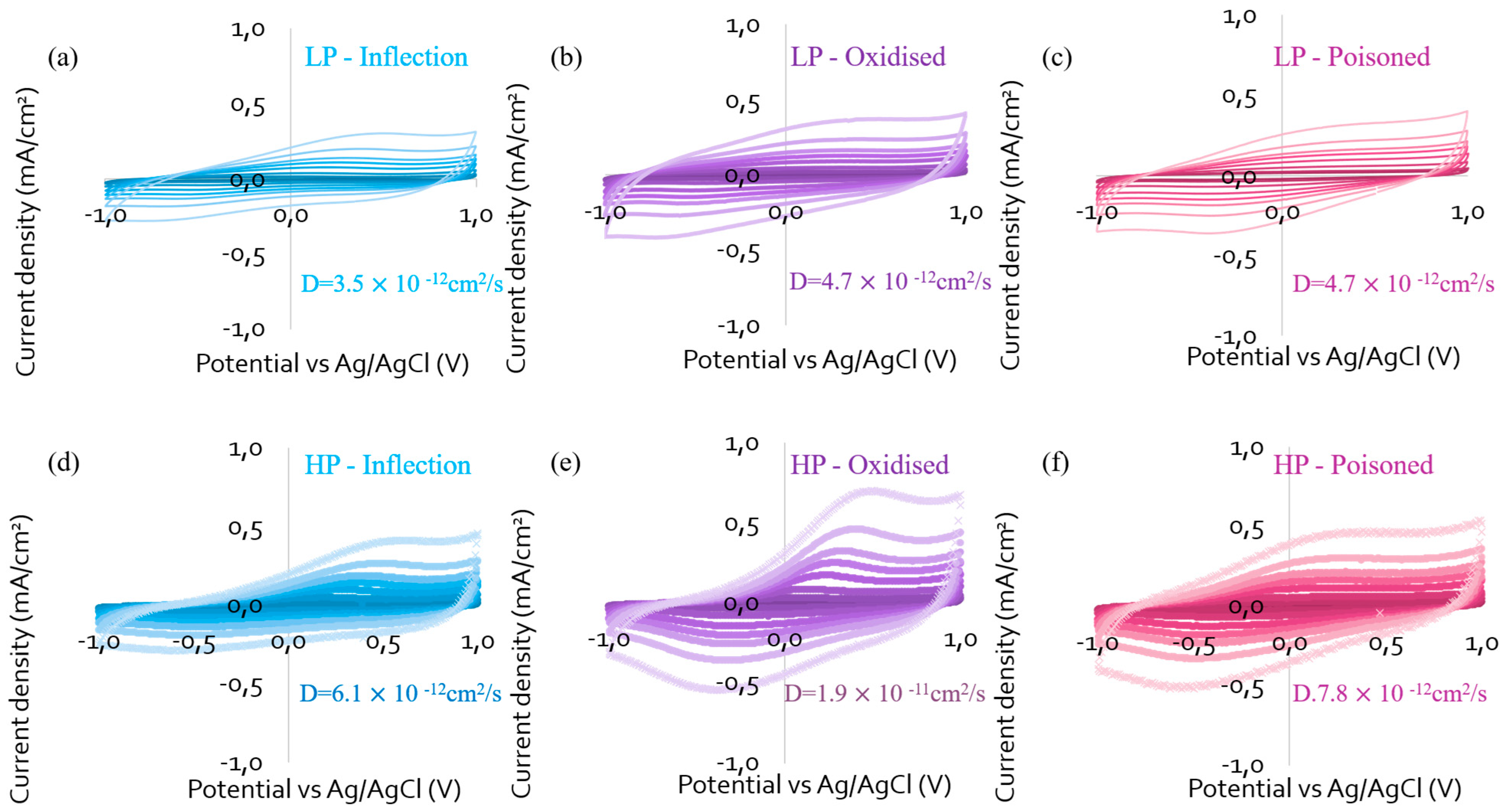
To evaluate the electrochemical performance of NiVxOy films, CV curves were performed (Figure 6), which represent the redox reaction of insertion/extraction of lithium ions from a 1 M LiClO4-PC electrolyte solution in the thin film, resulting in a colour change. The cathodic peak in the positive quadrant indicates the transition from Ni3+ (brown) to Ni2+ (transparent), and the anodic peak in the negative quadrant indicates the reversible process of conversion of Ni2+ back to Ni3+. All the NiVxOy films showed a similar CV curve shape but with differences in the value of the area under the curve (calculated by integration). Further understanding of the charge-storage and ion-transport mechanisms underlying the CV response was obtained by applying the Randles–Sevcik analysis used to estimate the ion transport behaviour, confirming the predominance of a mixed pseudocapacitive-diffusional response; the linearity plots of ip versus ν1/2 for all samples are provided in Figure S3. NiVxOy thin films deposited under high pressure and containing a high enough oxygen concentration (oxidised and poisoned P.E.M. points) showed the highest values of area and ion diffusion coefficient, leading to the optimal electrochromic behaviour. Avendaño et al. [65] also found that partly oxidised NiV coatings (as in the oxidised point considered here) showed the best EC properties when using a KOH electrolyte. Therefore, it is important to note that an appropriate choice of oxygen content is key for optimising the EC performance of NiVxOy coatings. Even when keeping the working pressure and the rest of the process parameters constant, adjusting the oxygen level can lead to a significant improvement in the ionic diffusion coefficient. Specifically, an increase of 143% is observed when comparing the highly oxidised condition (HP–poisoned, 7.8 × 10⁻¹² cm2/s) with the partly oxidised condition (HP–oxidised, 1.9 × 10⁻¹¹ cm2/s). The XRD patterns also support this observation, showing a well-defined crystalline structure (phase 111) against the polycrystalline structure characterised by a mixture of (111) and (200) phases from the poisoned sample. The pure (111) phase structure and the small crystallite size correlate with higher charge density and optical modulation, as such structures are generally considered favourable for ion transport [33,61]. Additionally, the surface microstructure and area of the film also have an influence on the EC performance, since the presence of cracks provides additional pathways for lithium ion transport during the redox process, as observed by other authors [22,61].
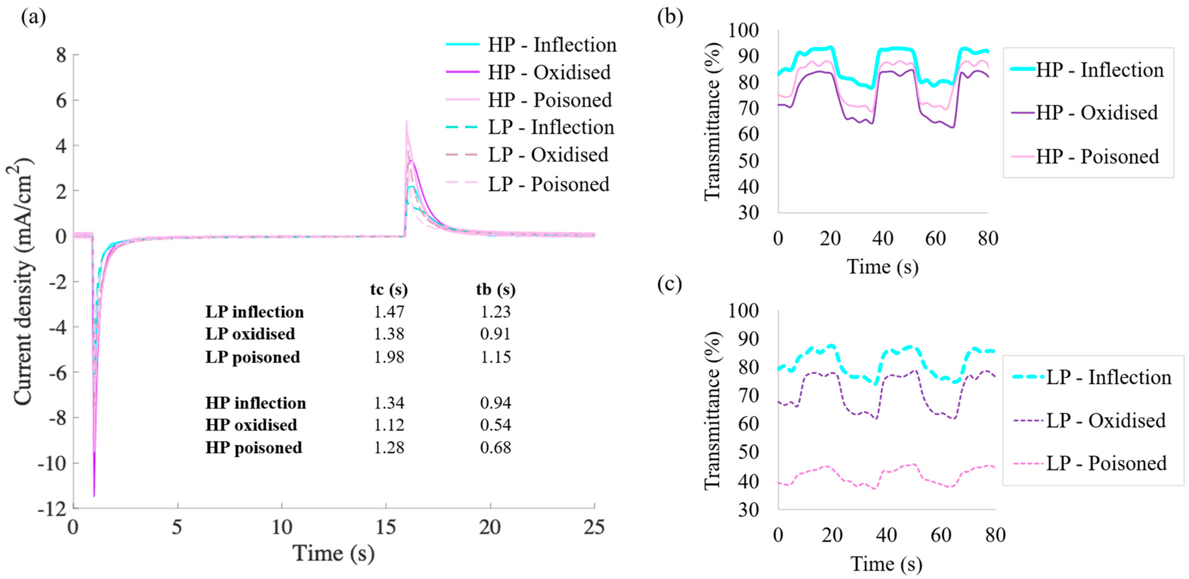
The electrochromic performance of the glass/ITO/NiVxOy samples is shown in Figure 7 and Table 2. These present two key parameters used to evaluate the behaviour of electrochromic coatings: the colouration efficiency (η), defined as the optical density change (ΔOD) per unit of inserted charge density, and the optical modulation (ΔT) of the different layers. Figure 7a shows the CA curves, where the thin films developed at the oxidated point present the highest charge density (Q), both under high and low pressure (4.0 and 3.5 mC/cm2, respectively), in contrast to the lowest Q values observed for the films deposited at the inflexion and poisoned points, ranging from 2.5 to 2.7 mC/cm2. In terms of response time, the films deposited at the oxidised P.E.M. point under high pressure exhibit the fastest kinetics, with colouration (tc) and bleaching times (tb) of 1.12 s and 0.54 s, respectively (HP-oxidised). In contrast, coatings grown at the inflexion point and under poisoned conditions show a significantly slower response, reaching up to 1.98 s for colouration and 1.15 s for bleaching in the LP-poisoned sample, with bleaching being the most affected process. Overall, HP deposited samples reveal shorter response times than their LP equivalents. In the literature, sputtered NiVxOy coatings exhibit higher colouration and bleaching times of approximately 3 s and 2 s, respectively, together with charge densities of10.16 mC/cm2 [38]. This difference can be attributed to the shorter characteristic ion transport length. In this regard, the NiVxOy layers investigated in the present study have a thickness of 150 nm, which is lower than the 200 nm reported by J. Ye et al. [38]. Since the characteristic diffusion time scales with the square of the diffusion length, the reduced thickness shortens the ion transport pathway and accelerates the charge accumulation process, resulting in shorter response times.
A comparison of Figure 7b,c reveals that transmittance modulation is primarily enhanced when the processes are carried out at HP, while the regulation of the O2 flux produces a significant improvement only for the films grown at LP. The coating deposited at high pressure and oxidised P.E.M. point presented the greatest ΔT of 21%. At low pressure, the electrochromic performance is significantly obstructed compared to HP conditions, reducing the optical contrast to 16%. This behaviour corresponds to a higher ion storage capacity, as also evidenced by the CV curves (Figure 6), and is consistent with the trends reported by Haonan Li et al. [22] for NiO-based layers deposited under different pressures. In their study, the authors demonstrated that this improvement is the result of the effect of structural stability and efficient ion transport within the film during the electrochemical cycle. A clear correlation between increased O2 content and enhanced colouration efficiency was observed, achieving a maximum value of 40 cm2/C for the HP-Poisoned-coated sample. This performance is comparable to previously reported values obtained using significantly thicker films (200 nm) and higher oxygen flow ratios (up to 40%) [37], while our process involved only 4% of O2 and 150 nm coating thickness. This suggests that the deposition method and plasma conditions used in this study enable an efficient film growth under milder conditions. Nevertheless, the efficiency of the deposited coating remains below the 63 cm2/C reported by Y.-S. Lin et al. [44] for 321 nm-thick films, likely due to the nearly doubled thickness used in their study, which enhances optical modulation. The coatings deposited at the poisoned P.E.M. point exhibit the highest colouring efficiency but the lowest Q values. Since, as mentioned in the introduction, NiVxOy coatings are primarily designed for ion storage, it is crucial to consider the balance between colouring efficiency and charge density when determining the optimal deposition process parameters. Accordingly, the NiVxOy coatings deposited at oxidised P.E.M. point (both at high and low pressure) demonstrated the best compromise between charge density and colouration efficiencies, leading the high pressure scenario to the best EC performance, with values in the range of 0.9 to 10 mC/cm2, consistent with values reported in the literature using LiClO4-based electrolytes [22,33,38,44].
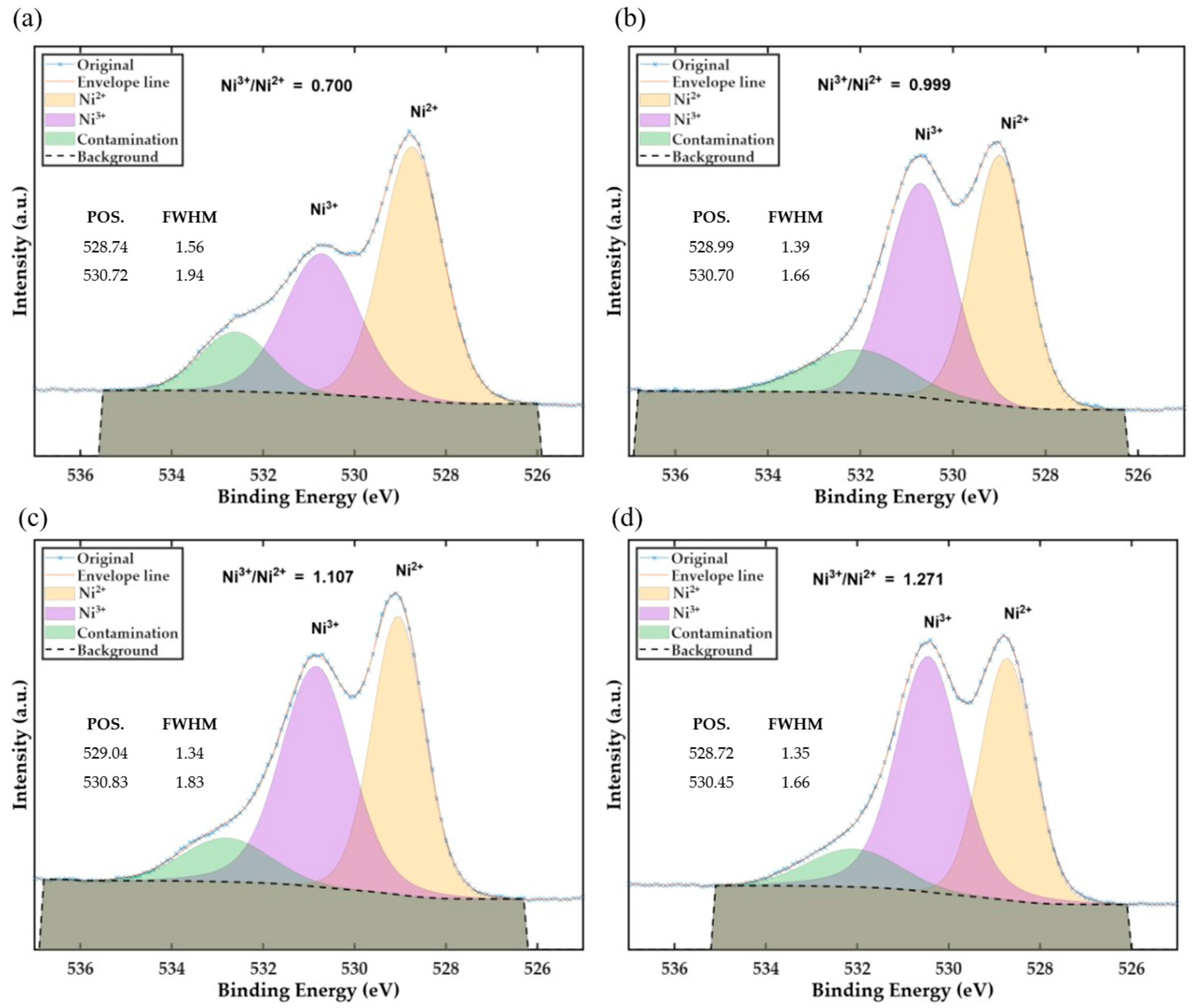
The samples that exhibited the highest EC capacities in terms of ΔOD and n (oxidised and poisoned P.E.M. points) were analysed by XPS (Figure 8 and Figure 9) to determine the coating composition and the relative proportions of Ni3+ and Ni2+. To estimate the proportion of NiO and Ni2O3 in nonstoichiometric NiVxOy films, the O1s spectra in Figure 8 were deconvoluted into three peaks: NiO (528.8 eV), Ni2O3 (530.5 eV), and a third attributed to the surface contamination, such as carbon oxides and H-O-H bond for the residual water (532 eV) [32,62,66,67]. For the proportion of different vanadium states in the thin films, the V 2p3/2 spectrum was deconvoluted into three distinct peaks at 513.6 eV, 515.8 eV and 516.9 eV [68], which correspond to the V2+ (VO), V3+ (V2O3) and V5+ (V2O5) oxidation states, respectively. Figure 8 reveals that the higher the O2 flux, the higher the Ni3+ concentration. This shows that a high oxygen content leads to the incorporation of interstitial oxygen, which results in the formation of Ni2+ vacancies. To maintain charge neutrality, Ni2+ ions are partially oxidised to Ni3+, introducing holes into the lattice. This increase in the Ni3+/Ni2+ ratio promotes the development of non-stoichiometric phases and point defects, contributing to higher hole concentrations and a reduction in optical transmission (Figure 5). As discussed in the electrochromic analysis, the enhanced hole density due to Ni3+ formation facilitates ion and electron transport during charging and discharging, thereby improving the electrochromic performance of the film.
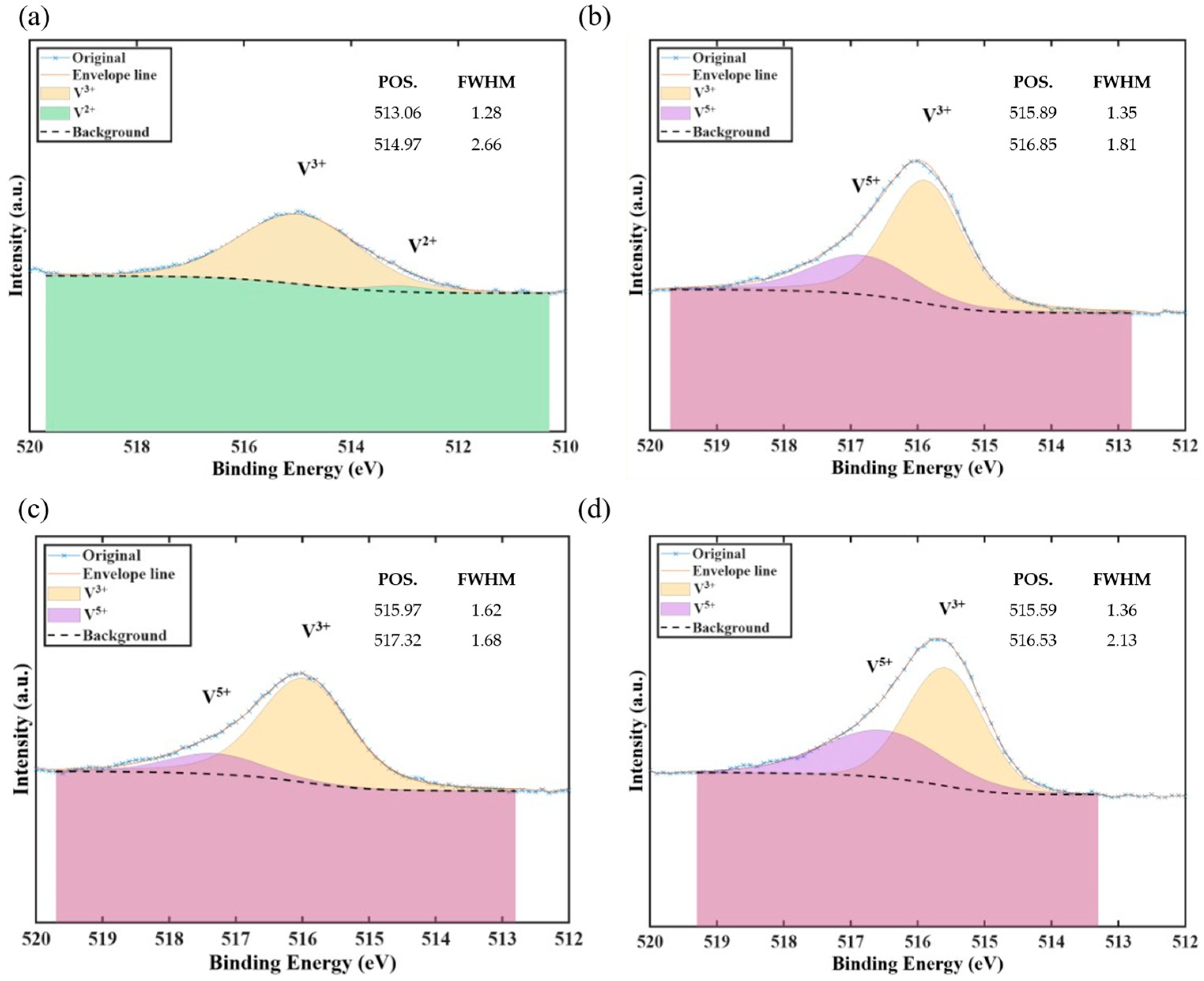
As observed for nickel in Figure 8, where increasing oxygen content and pressure correlated with a higher concentration of Ni3+ species, a similar trend is evident in Figure 9 for vanadium. This figure presents the spectra of the thin NiVxOy films deposited under the four experimental conditions considered. The analysis confirms the presence of vanadium in multiple oxidation states, with V2+, V3+, and V5+ species detected within the binding energy range of 519 eV to 512 eV. It is observed that increasing the O2 flux from oxidised to poisoned point during deposition leads to an increase in the V5+ signal intensity. These results agree with those reported by A. Rakshit et al. [69], who found that a higher oxygen availability during film growth stabilises the higher oxidation states of V. Furthermore, it was also observed that despite a higher O2 flux at the oxidised point under low-pressure (LP) conditions, samples processed at higher chamber pressure exhibit a higher fraction of V5+. This phenomenon is attributed to the longer residence time of oxygen species within the vacuum chamber at elevated pressures, which allows for more complete oxidation reactions before gas evacuation.
In addition, the surface atomic composition was quantified (Table 3) from the XPS survey spectra (Figure S4). The vanadium content remains low and nearly constant for all samples (2.0–2.7 at.%), yielding an average Ni/V ratio close to 10, which indicates that the incorporation of vanadium is stable and not significantly affected by the deposition conditions. By normalising the atomic concentrations to Ni = 1, the surface composition can be approximated as NiVxOy, with x ≈ 0.10 for all samples, while the oxygen, y coefficient, increases from ~2.5 under less oxidising conditions to ~4.0 for the most oxidising conditions, confirming a progressive oxidation of the films. Therefore, the increase in the V5+ contribution observed in Figure 9 is attributed to an oxidation of vanadium species promoted by higher oxygen availability and pressure, and not to an enrichment in vanadium concentration at the surface.

3.4. Short-Term Cycling Stability of NiVxOy Electrochromic Coatings

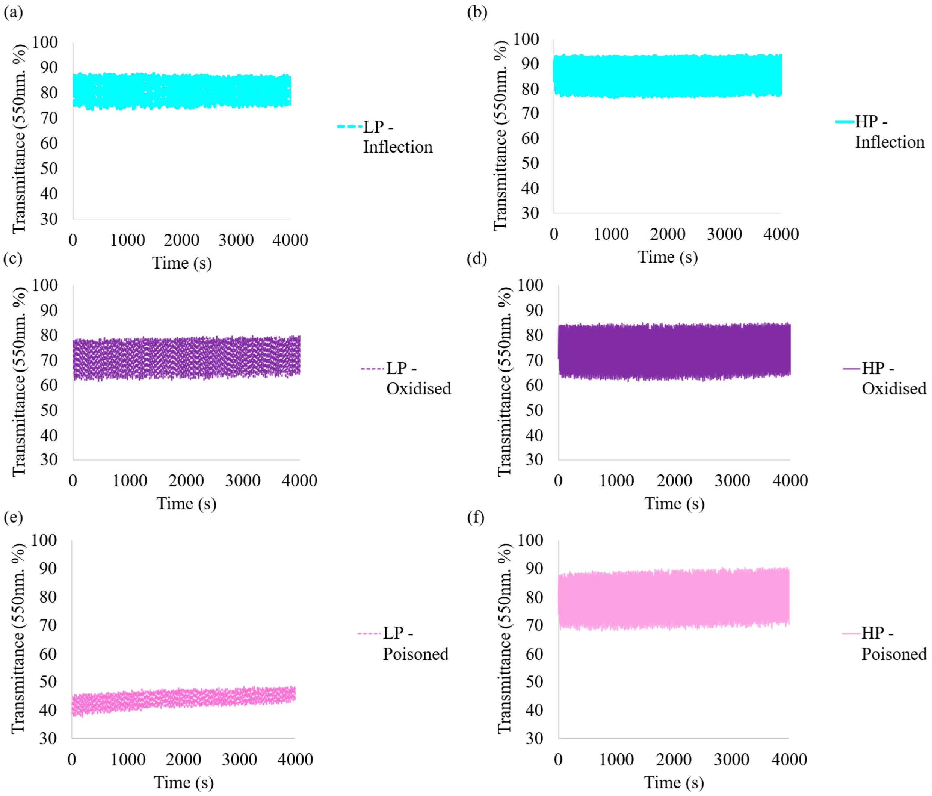
The evaluation of cycling durability is key to the validation of the optical performance of electrochromic coatings under operational conditions. A CA cycling test was carried out for 4000 s using ±1 V steps of 15 s in order to examine the short-term stability of the optical modulation and to enable a direct comparison between films deposited under different target oxidation states. The transmission results shown in Figure 10 confirm the stability of the coating in spite of the presence of surface cracks, without observing a loss of transmittance modulation during this timeframe. Although previous studies have reported that a high density of surface cracks in NiO coatings can lead to increased degradation of optical modulation during prolonged cycling [22,61], the results here showed no evidence of such deterioration under the present short-term test conditions. In contrast, a previous study on WOx or NiO films showed measurable degradation even during short-term cycling, which was attributed to the larger crack density in those coatings [35,48]. In the present results, the absence of early degradation is probably related to the superficial nature of the cracks, which were not observed inside the thin film, as also reported by Li H. et al. for coating developed at 2.4 Pa [22]. On the contrary, these features may have contributed positively to the EC performance by increasing the electrochemically active surface area, indicating that the electrochromic reaction of NiO mainly occurs on the crystal surface, as also reported in recent reviews on NiO-based and advanced electrochromic materials [70,71]. It should be noted, however, that confirming whether this behaviour is maintained over the full operational lifetime of an electrochromic device would require durability tests over longer cycling times.
The reduction in transmittance observed in Figure 5 and Figure 10 for LP coatings can be attributed to two distinct effects (see Figure S5). First, as discussed in Section 3.2, the variation among control points is mainly due to the increase in Ni3+ content. Second, the pressure-related effect observed for LP coatings is associated with a higher concentration of V3+, as evidenced in Figure 9. This increased V3+ content enhances light absorption attributed to electronic transitions between d-type bands, which is in line with observations on vanadium oxide films during electrochemical cycling, where the presence of V3+ correlates with blue colouration and strong absorption in the visible range [72].

4. Conclusions

An OES-based method for monitoring the deposition of functional thin films by RMS has been applied to produce EC NiVxOy coatings. The Ni target discharge voltage has shown non-monotonic behaviour, which complicates control in regions where the process gain changes sign. In contrast, OES has demonstrated a monotonic response, allowing simpler feedback control since the process gain does not change sign, and the control could be established with simple PID parameters.
This work presents an investigation of multiple P.E.M. operating regimes along the reactive sputtering hysteresis curve and demonstrates their distinct impact on deposition kinetics, film composition, microstructure and electrochromic performance. The process parameters that provide the best compromise between optical modulation and charge density were a high pressure and 30% of Ni P.E.M. signal, which resulted in a high Ni3+ proportion, low V5+ content and surface cracks at low density. Under these conditions, the coatings exhibit a preferential (111) orientation with a crystallite size of 13.7 nm and a compact tetrahedral-like microstructure, which promotes efficient ion transport and a high density of electrochemically active sites. As a result, very short response times are achieved, with colouration and bleaching times of 1.12 s and 0.54 s, respectively, confirming the beneficial electrochromic kinetics associated with this microstructural configuration. These results should therefore be interpreted within the timeframe investigated in this study, as long-term cycling behaviour may differ.
In terms of industrial applicability, the simplicity of the OES technique has a significant impact on processes with large targets and requiring a specific O2 ratio, where a user-friendly method is essential.

Supplementary Materials

The following supporting information can be downloaded at: https://www.mdpi.com/article/10.3390/coatings16020206/s1, Figure S1. Optical emission spectrum of the plasma generated from a NiV target; Figure S2. Time evolution during reactive control at different set-points using the PEM-based reactive sputtering control technology, showing the initial 10 min of Ar target cleaning and the subsequent deposition stages for each control point; Figure S3. Peak current dependence on scan rate square root (ip vs. ν1/2) showing linear trends for HP and LP NiVxOy films under different oxidation conditions; Figure S4. XPS survey spectra of HP and LP NiVxOy films under different oxidation conditions; Figure S5. Atomic concentration of Ni2+, Ni3+, V3+ and V5+ in NiVxOy films obtained from XPS spectra, with an inset zoom on vanadium species.

Author Contributions

Conceptualization, I.Q.; Methodology, O.H.-R. and G.G.; Investigation, O.H.-R.; Writing—original draft preparation, O.H.-R.; Writing—review and editing, O.H.-R., G.G., R.O., E.Z., V.B.-G. and E.G.-B.; Supervision, I.Q.; Funding acquisition, I.Q. All authors have read and agreed to the published version of the manuscript.

Funding

This research was funded by CDTI (Centro para el Desarrollo Tecnológico Industrial) in the SURFERA-PLUS project (EXP—00163512/CER-20231008) in frames of the CERVERA program 2023 (https://www.surfera-plus.com, accessed on 4 February 2026).

Data Availability Statement

The remaining experimental data generated by the authors are available from the corresponding author upon reasonable request.

Acknowledgments

E. Z. thanks funding from the Basque Government Department of Education, University and Research (consolidated research groups IT-1766-22 GIC21/131).

Conflicts of Interest

Author Victor Bellido-Gonzalez was employed by the company “Gencoa Ltd.”. The remaining authors declare that the research was conducted in the absence of any commercial or financial relationships that could be construed as a potential conflict of interest.

Abbreviations

The following abbreviations are used in this manuscript:
AVTAverage visible transmittance
CAChronoamperometry
CEColouration efficiency
CVCyclic voltammetry
DCDirect current
ECDElectrochromic device
ECElectrochromic
FE-SEMField emission scanning electron microscopy
FWHMFull width at half maximum
HPHigh pressure
LPLow pressure
MFCMass flow controller
MSMagnetron sputtering
OESOptical emission spectroscopy
P.E.MPlasma emission monitoring
PDFPseudo-derivative feedback
RMSReactive magnetron sputtering
SEMScanning electron microscopy
XPSX-ray photoelectron spectroscopy
XRDX-ray diffraction

References

  1. Huang, Y.; Wang, B.; Chen, F.; Han, Y.; Zhang, W.; Wu, X.; Li, R.; Jiang, Q.; Jia, X.; Zhang, R. Electrochromic Materials Based on Ions Insertion and Extraction. Adv. Opt. Mater. 2022, 10, 2101783. [Google Scholar] [CrossRef] [Scilit]
  2. Cannavale, A.; Cossari, P.; Eperon, G.E.; Colella, S.; Fiorito, F.; Gigli, G.; Snaith, H.J.; Listorti, A. Forthcoming Perspectives of Photoelectrochromic Devices: A Critical Review. Energy Environ. Sci. 2016, 9, 2682–2719. [Google Scholar] [CrossRef] [Scilit]
  3. Patel, K.J.; Bhatt, G.G.; Ray, J.R.; Suryavanshi, P.; Panchal, C.J. All-Inorganic Solid-State Electrochromic Devices: A Review. J. Solid State Electrochem. 2017, 21, 337–347. [Google Scholar] [CrossRef] [Scilit]
  4. Rai, V.; Singh, R.S.; Blackwood, D.J.; Zhili, D. A Review on Recent Advances in Electrochromic Devices: A Material Approach. Adv. Eng. Mater. 2020, 22, 2000082. [Google Scholar] [CrossRef] [Scilit]
  5. Mehmood, A.; Long, X.; Haidry, A.A.; Zhang, X. Trends in Sputter Deposited Tungsten Oxide Structures for Electrochromic Applications: A Review. Ceram. Int. 2020, 46, 23295–23313. [Google Scholar] [CrossRef] [Scilit]
  6. Granqvist, C.G.; Arvizu, M.A.; Pehlivan, İ.B.; Qu, H.Y.; Wen, R.T.; Niklasson, G.A. Electrochromic Materials and Devices for Energy Efficiency and Human Comfort in Buildings: A Critical Review. Electrochim. Acta 2018, 259, 1170–1182. [Google Scholar] [CrossRef] [Scilit]
  7. Modak, M.; Rane, S.; Jagtap, S. WO 3: A Review of Synthesis Techniques, Nanocomposite Materials and Their Morphological Effects for Gas Sensing Application. Bull. Mater. Sci. 2023, 46, 28. [Google Scholar] [CrossRef] [Scilit]
  8. Gillaspie, D.T.; Tenent, R.C.; Dillon, A.C. Metal-Oxide Films for Electrochromic Applications: Present Technology and Future Directions. J. Mater. Chem. 2010, 20, 9585–9592. [Google Scholar] [CrossRef] [Scilit]
  9. Zhang, W.; Li, H.; Hopmann, E.; Elezzabi, A.Y. Nanostructured Inorganic Electrochromic Materials for Light Applications. Nanophotonics 2020, 10, 825–850. [Google Scholar] [CrossRef] [Scilit]
  10. Wu, S.; Sun, H.; Duan, M.; Mao, H.; Wu, Y.; Zhao, H.; Lin, B. Applications of Thermochromic and Electrochromic Smart Windows: Materials to Buildings. Cell Rep. Phys. Sci. 2023, 4, 101370. [Google Scholar] [CrossRef] [Scilit]
  11. Access, O.; Hussein, H.S. The State of the Art of Nanomaterials and Its Applications in Energy Saving. Bull. Natl. Res. Cent. 2023, 47, 7. [Google Scholar] [CrossRef] [Scilit]
  12. Ghosh, T.; Kandpal, S.; Rani, C.; Chaudhary, A.; Kumar, R. Recipe for Fabricating Optimized Solid-State Electrochromic Devices and Its Know-How: Challenges and Future. Adv. Opt. Mater. 2023, 11, 2203126. [Google Scholar] [CrossRef] [Scilit]
  13. Yang, P.; Sun, P.; Mai, W. Electrochromic Energy Storage Devices. Mater. Today 2016, 19, 394–402. [Google Scholar] [CrossRef] [Scilit]
  14. Yang, G.; Zhang, Y.M.; Cai, Y.; Yang, B.; Gu, C.; Zhang, S.X.A. Advances in Nanomaterials for Electrochromic Devices. Chem. Soc. Rev. 2020, 49, 8687–8720. [Google Scholar] [CrossRef] [Scilit] [PubMed]
  15. Sibilio, S.; Rosato, A.; Scorpio, M.; Iuliano, G.; Ciampi, G.; Vanoli, G.P.; De Rossi, F. A Review of Electrochromic Windows for Residential Applications. Int. J. Heat Technol. 2016, 34, S481–S488. [Google Scholar] [CrossRef] [Scilit]
  16. Granqvist, C.G. Electrochromics for Smart Windows: Oxide-Based Thin Films and Devices. Thin Solid Film. 2014, 564, 1–38. [Google Scholar] [CrossRef] [Scilit]
  17. Granqvist, C.G. (Ed.) Handbook of Inorganic Electrochromic Materials, 1st ed.; Elsevier: Amsterdam, The Netherlands, 1995; ISBN 978-0-444-89930-9. [Google Scholar]
  18. Passerini, S.; Scrosati, B.; Gorenstein, A. The Intercalation of Lithium in Nickel Oxide and Its Electrochromic Properties. Electrochem. Soc. 1990, 137, 10. [Google Scholar] [CrossRef] [Scilit]
  19. Wei, Y.; Chen, M.; Liu, W.; Li, L.; Yan, Y. Electrochemical Investigation of Electrochromic Devices Based on NiO and WO3 Films Using Different Lithium Salts Electrolytes. Electrochim. Acta 2017, 247, 107–115. [Google Scholar] [CrossRef] [Scilit]
  20. Xuping, Z.; Haokang, Z.; Qing, L.; Hongli, L. All-Solid-State Inorganic Electrochromic Display of WO3 and NiO Films with LiNbO3 Ion Conductor. IEEE Electron Device Lett. 2000, 21, 215–217. [Google Scholar] [CrossRef]
  21. Xie, Z.; Liu, Q.; Zhang, Q.; Lu, B.; Zhai, J.; Diao, X. Fast-Switching Quasi-Solid State Electrochromic Full Device Based on Mesoporous WO3 and NiO Thin Films. Sol. Energy Mater. Sol. Cells 2019, 21, 215–217. [Google Scholar] [CrossRef] [Scilit]
  22. Li, H.; Li, Y.; Li, X.; Xie, A.; Sun, D.; Wang, Y. Effects of Sputtering Pressure on Electrochromic Properties of NiO Films Prepared by DC Magnetron Sputtering. J. Electrochem. Soc. 2022, 169, 116508. [Google Scholar] [CrossRef] [Scilit]
  23. Shin, M.; Lee, J.H.; Seo, I.; Kang, H.W.; Seo, J.H.; Jin, H.J.; Kim, B.H.; Tenent, R.C.; Han, S.H. Durability Enhancement of All-Solid-State Electrochromic Devices by Adjusting the Charge Density Ratio between Electrochromic and Counter Electrode Layers. Sol. Energy Mater. Sol. Cells 2024, 272, 112901. [Google Scholar] [CrossRef] [Scilit]
  24. Ukoba, K.O.; Eloka-Eboka, A.C.; Inambao, F.L. Review of Nanostructured NiO Thin Film Deposition Using the Spray Pyrolysis Technique. Renew. Sustain. Energy Rev. 2018, 82, 2900–2915. [Google Scholar] [CrossRef] [Scilit]
  25. Obaida, M.; Fathi, A.M.; Moussa, I.; Afify, H.H. Characterization and Electrochromic Properties of NiO Thin Films Prepared Using a Green Aqueous Solution by Pulsed Spray Pyrolysis Technique. J. Mater. Res. 2022, 37, 2282–2292. [Google Scholar] [CrossRef] [Scilit]
  26. Sahu, D.R.; Lee, Y.H.; Wu, T.J.; Wang, S.C.; Huang, J.L. Synthesis and Electrochromic Property Improvement of NiO Films for Device Applications. Thin Solid Film. 2020, 707, 138097. [Google Scholar] [CrossRef] [Scilit]
  27. Sahu, D.R.; Wu, T.J.; Wang, S.C.; Huang, J.L. Electrochromic Behavior of NiO Film Prepared by E-Beam Evaporation. J. Sci. Adv. Mater. Devices 2017, 2, 225–232. [Google Scholar] [CrossRef] [Scilit]
  28. Pereira, S.; Gonçalves, A.; Correia, N.; Pinto, J.; Pereira, L.; Martins, R.; Fortunato, E. Electrochromic Behavior of NiO Thin Films Deposited by E-Beam Evaporation at Room Temperature. Sol. Energy Mater. Sol. Cells 2014, 120, 109–115. [Google Scholar] [CrossRef] [Scilit]
  29. Saadeddin, I.; Suleiman, M.; Salman, H.; Zrikem, K.; Song, G.; Rougier, A. Optimization of Low Value Electrodeposition Parameters of Nano-Structured NiO Electrochromic Thin Films. Solid State Ion. 2019, 343, 115129. [Google Scholar] [CrossRef] [Scilit]
  30. Jin, S.; Wen, S.; Li, M.; Zhong, H.; Chen, Y.; Wang, H. Effect of the Grain Size on the Electrochromic Properties of NiO Films. Opt. Mater. 2020, 109, 110280. [Google Scholar] [CrossRef] [Scilit]
  31. Rakibuddin, M.; Shinde, M.A.; Kim, H. Sol-Gel Fabrication of NiO and NiO/WO3 Based Electrochromic Device on ITO and Flexible Substrate. Ceram. Int. 2020, 46, 8631–8639. [Google Scholar] [CrossRef] [Scilit]
  32. Dalavi, D.S.; Devan, R.S.; Patil, R.S.; Ma, Y.R.; Patil, P.S. Electrochromic Performance of Sol-Gel Deposited NiO Thin Film. Mater. Lett. 2013, 90, 60–63. [Google Scholar] [CrossRef] [Scilit]
  33. Tang, Y.; Shen, H.; Wang, T.; Peng, S.; Jin, K.; Qian, Q.; Li, G.; Gan, Z. Study on Electrochemical Ion Behavior and Electrochromic Properties of NiO Thin Films Prepared by Magnetron Sputtering with Different Oxygen Levels. Thin Solid Film. 2023, 769, 139754. [Google Scholar] [CrossRef] [Scilit]
  34. Zhang, L.; Chen, Z.; Ma, H. Effect of Sputtering Pressure and Oxygen Content on the Electrochromic Properties of NiO Films by DC Magnetron Sputtering. Phys. B Condens. Matter 2024, 677, 415663. [Google Scholar] [CrossRef] [Scilit]
  35. Ding, Y.; Wang, M.; Mei, Z.; Liu, L.; Yang, J.; Zhong, X.; Wang, M.; Diao, X. Electrochromic Adaptability of NiOx Films Modified by Substrate Temperature in Aqueous and Non-Aqueous Electrolytes. Adv. Mater. Interfaces 2022, 9, 2102223. [Google Scholar] [CrossRef] [Scilit]
  36. Igartua, A.; Mendoza, G.; Fernandez, X.; Zabala, B.; Alberdi, A.; Bayon, R.; Aranzabe, A. Surface Treatments Solutions to Green Tribology. Coatings 2020, 10, 634. [Google Scholar] [CrossRef] [Scilit]
  37. Liang, J.; Liu, Q.; Li, T.; Luo, Y.; Lu, S.; Shi, X.; Zhang, F.; Asiri, A.M.; Sun, X. Magnetron Sputtering Enabled Sustainable Synthesis of Nanomaterials for Energy Electrocatalysis. Green Chem. 2021, 23, 2834–2867. [Google Scholar] [CrossRef] [Scilit]
  38. Ye, J.M.; Lin, Y.P.; Yang, Y.T.; Chang, J.T.; He, J.L. Electrochromic Properties of Ni(V)Ox Films Deposited via Reactive Magnetron Sputtering with a 8V-92Ni Alloy Target. Thin Solid Film. 2010, 519, 1578–1582. [Google Scholar] [CrossRef] [Scilit]
  39. Weng, K.W.; Lin, T.N.; Huang, J.J.; Huang, Y.P. Deposition of NiVOx Thin Films by Pulse Magnetron Sputtering with Various Ar/O2 Ratios. Thin Solid Film. 2013, 529, 62–65. [Google Scholar] [CrossRef] [Scilit]
  40. Niklasson, G.A.; Granqvist, C.G. Electrochromics for Smart Windows: Thin Films of Tungsten Oxide and Nickel Oxide, and Devices Based on These. J. Mater. Chem. 2007, 17, 127–156. [Google Scholar] [CrossRef] [Scilit]
  41. Lin, H.; Wang, Z.; Han, Q.; Wang, R.; Pan, L.; Zhu, H.; Wan, M.; Mai, Y. The Growth, Properties and Application of Reactively Sputtered Nickel Oxide Thin Films in All Thin Film Electrochromic Devices. Mater. Sci. Eng. B Solid. State. Mater. Adv. Technol. 2021, 270, 115196. [Google Scholar] [CrossRef] [Scilit]
  42. Keraudy, J.; García Molleja, J.; Ferrec, A.; Corraze, B.; Richard-Plouet, M.; Goullet, A.; Jouan, P.Y. Structural, Morphological and Electrical Properties of Nickel Oxide Thin Films Deposited by Reactive Sputtering. Appl. Surf. Sci. 2015, 357, 838–844. [Google Scholar] [CrossRef] [Scilit]
  43. Karpinski, A.; Ferrec, A.; Richard-Plouet, M.; Cattin, L.; Djouadi, M.A.; Brohan, L.; Jouan, P.Y. Deposition of Nickel Oxide by Direct Current Reactive Sputtering: Effect of Oxygen Partial Pressure. Thin Solid Film. 2012, 520, 3609–3613. [Google Scholar] [CrossRef] [Scilit]
  44. Lin, Y.S.; Chen, P.W.; Lin, D.J. Electrochromic Performance of NiVxOy Thin Films Deposited onto Flexible PET/ITO Substrates by Reactive Plasma Sputtering for Flexible Electrochromic Devices. Thin Solid Film. 2010, 518, 7416–7420. [Google Scholar] [CrossRef] [Scilit]
  45. Han, Y.H.; Jung, S.J.; Lee, J.J. Deposition of TiO2 Films by Reactive Inductively Coupled Plasma Assisted DC Magnetron Sputtering for High Crystallinity and High Deposition Rate. Surf. Coat. Technol. 2007, 201, 5387–5391. [Google Scholar] [CrossRef] [Scilit]
  46. Bellido-Gonzalez, V.; Daniel, B.; Monaghan, D.; Counsell, J. Uniformity Control in Reactive Magnetron Sputtering. In Proceedings of the Glass Performance Days, Tampere, Finland, 12–15 June 2009; pp. 1–4. [Google Scholar]
  47. Sgrilli, T. Reactive Magnetron Sputtering Feedback Control Via Target Voltage: A Method to Overcome Ambiguities in Complex Systems. In 66th Annual Technical Conference Proceedings; Society of Vacuum Coaters: Albuquerque, NM, USA, 2023; Volume 66. [Google Scholar] [CrossRef] [Scilit]
  48. Hernandez-Rodriguez, O.; Guzman, G.; Ortiz, R.; Zuza, E.; Bellido-Gonzalez, V.; Quintana, I.; G-Berasategui, E. OES-Based Control Methodology for Process Optimization of WOx Electrochromic Coatings Deposited by Reactive Magnetron Sputtering. Surf. Coat. Technol. 2025, 511, 132239. [Google Scholar] [CrossRef] [Scilit]
  49. Bellido-González, V.; Daniel, B.; Counsell, J.; Monaghan, D. Reactive Gas Control of Non-Stable Plasma Conditions. Thin Solid Film. 2006, 502, 34–39. [Google Scholar] [CrossRef] [Scilit]
  50. Dong, D.; Wang, W.; Dong, G.; Zhang, F.; He, Y.; Yu, H.; Liu, F.; Wang, M.; Diao, X. Electrochromic Properties and Performance of NiOx Films and Their Corresponding All-Thin-Film Flexible Devices Preparedby Reactive DC Magnetron Sputtering. Appl. Surf. Sci. 2016, 383, 49–56. [Google Scholar] [CrossRef] [Scilit]
  51. Depla, D.; Heirwegh, S.; Mahieu, S.; Haemers, J.; De Gryse, R. Understanding the Discharge Voltage Behavior During Reactive Sputtering of Oxides. J. Appl. Phys. 2007, 101, 013301. [Google Scholar] [CrossRef] [Scilit]
  52. Depla, D.; Buyle, G.; Haemers, J.; De Gryse, R. Discharge Voltage Measurements during Magnetron Sputtering. Surf. Coat. Technol. 2006, 200, 4329–4338. [Google Scholar] [CrossRef] [Scilit]
  53. Audronis, M.; Bellido-Gonzalez, V. Hysteresis Behaviour of Reactive High Power Impulse Magnetron Sputtering. Thin Solid Film. 2010, 518, 1962–1965. [Google Scholar] [CrossRef] [Scilit]
  54. Särhammar, E.; Nyberg, T.; Berg, S. Applying “the Upgraded Berg Model” to Predict Hysteresis Free Reactive Sputtering. Surf. Coat. Technol. 2016, 290, 34–38. [Google Scholar] [CrossRef] [Scilit]
  55. Kakati, H.; Borah, S.M. Study of Hysteresis Behavior in Reactive Sputtering of Cylindrical Magnetron Plasma. Chin. Phys. B 2015, 24, 125201. [Google Scholar] [CrossRef] [Scilit]
  56. Pflug, A.; Siemers, M.; Szyszka, B.; Severin, D.; Physikalisches, I. A Second Hysteresis Effect of Reactive Magnetron Sputtering in Compound Mode. In Proceedings of the 49th Annual Technical Conference of the Society of Vacuum Coaters, Society of Vacuum Coaters, Washington, DC, USA, 22–27 April 2006; pp. 434–440. [Google Scholar]
  57. Berg, S.; Blom, H.-O.; Larsson, T.; Nender, C. Modeling of Reactive Sputtering of Compound Materials. J. Vac. Sci. Technol. A Vac. Surf. Film. 1987, 5, 202–207. [Google Scholar] [CrossRef] [Scilit]
  58. Strijckmans, K.; Schelfhout, R.; Depla, D. Tutorial: Hysteresis during the Reactive Magnetron Sputtering Process. J. Appl. Phys. 2018, 124, 241101. [Google Scholar] [CrossRef] [Scilit]
  59. Weng, K.W.; Chen, Y.C.; Lin, T.N.; Li, Y.D.; Chen, T.L. Characterization of Ni0.92V0.08Ox Thin Films Deposited by the Pulse Sputter Method. Vacuum 2013, 87, 169–173. [Google Scholar] [CrossRef] [Scilit]
  60. Kotta, A.; Seo, H.K. Facile Synthesis of Highly Conductive Vanadium-Doped NiO Film for Transparent Conductive Oxide. Appl. Sci. 2020, 10, 5415. [Google Scholar] [CrossRef] [Scilit]
  61. Qiu, J.; Chen, Z.; Zhao, T.; Chen, Z.; Chu, W.; Yuan, N.; Ding, J. Effect of O 2 Concentration on the Electrochromic Properties of NiO x Films. J. Nanosci. Nanotechnol. 2017, 18, 4814–4821. [Google Scholar] [CrossRef] [Scilit]
  62. Tuna, Ö.; Mak, A.K.; Öztürk, O.; Karabulut, M. Influence of Oxygen Partial Pressure on the Structural, Optical and Electrochromic Properties of NiO Thin Films Grown by Magnetron Sputtering. Appl. Phys. A Mater. Sci. Process. 2023, 129, 820. [Google Scholar] [CrossRef] [Scilit]
  63. Hwang, J.D.; Ho, T.H. Effects of Oxygen Content on the Structural, Optical, and Electrical Properties of NiO Films Fabricated by Radio-Frequency Magnetron Sputtering. Mater. Sci. Semicond. Process. 2017, 71, 396–400. [Google Scholar] [CrossRef] [Scilit]
  64. Salunkhe, P.; Muhammed Ali, A.V.; Kekuda, D. Investigation on Tailoring Physical Properties of Nickel Oxide Thin Films Grown by Dc Magnetron Sputtering. Mater. Res. Express 2020, 7, 016427. [Google Scholar] [CrossRef] [Scilit]
  65. Avendaño, E.; Azens, A.; Isidorsson, J.; Karmhag, R.; Niklasson, G.A.; Granqvist, C.G. Optimized Nickel-Oxide-Based Electrochromic Thin Films. Solid State Ion. 2003, 165, 169–173. [Google Scholar] [CrossRef] [Scilit]
  66. Acuña, J.R.A.; Perez, I.; Sosa, V.; Gamboa, F.; Elizalde, J.T.; Farías, R.; Carrillo, D.; Enríquez, J.L.; Burrola, A.; Mani, P. Sputtering Power Effects on the Electrochromic Properties of NiO Films. Optik 2021, 231, 166509. [Google Scholar] [CrossRef] [Scilit]
  67. Payne, B.P.; Biesinger, M.C.; McIntyre, N.S. The Study of Polycrystalline Nickel Metal Oxidation by Water Vapour. J. Electron Spectros. Relat. Phenom. 2009, 175, 55–65. [Google Scholar] [CrossRef] [Scilit]
  68. Hryha, E.; Rutqvist, E.; Nyborg, L. Stoichiometric Vanadium Oxides Studied by XPS. Surf. Interface Anal. 2012, 44, 1022–1025. [Google Scholar] [CrossRef] [Scilit]
  69. Rakshit, A.; Mukherjee, M.; Chakraborty, S. Effect of Oxygen Content on the Electrical Properties of Sputter Deposited Vanadium Oxide Thin-Films. Mater. Sci. Semicond. Process. 2018, 88, 127–131. [Google Scholar] [CrossRef] [Scilit]
  70. Zhao, F.; Chen, T.; Zeng, Y.; Chen, J.; Zheng, J.; Liu, Y.; Han, G. Nickel Oxide Electrochromic Films: Mechanisms, Preparation Methods, and Modification Strategies-a Review. J. Mater. Chem. C Mater. 2024, 12, 7126–7145. [Google Scholar] [CrossRef] [Scilit]
  71. Wang, Z.; Zhu, H.; Zhuang, J.; Lu, Y.; Chen, Z.; Guo, W. Recent Advance in Electrochromic Materials and Devices for Display Applications. Chempluschem 2024, 89, e202300770. [Google Scholar] [CrossRef] [Scilit]
  72. Mjejri, I.; Gaudon, M.; Song, G.; Labrugère, C.; Rougier, A. Crystallized V2O5 as Oxidized Phase for Unexpected Multicolor Electrochromism in V2O3 Thick Film. ACS Appl. Energy Mater. 2018, 1, 2721–2729. [Google Scholar] [CrossRef] [Scilit]
Figure 1. Hysteresis curves of the Ni plasma emission intensity (% P.E.M. sensor signal monitoring at 352.3 nm Ni signal, blue solid line) and NiV target discharge voltage (% signal, red dotted line) as a function of the oxygen flow (purple dashed line) for the two experimental conditions: (a) high pressure (2.0 Pa, pumping speed 115 L/s) and (b) low pressure (0.6 Pa, pumping speed 398 L/s); P.E.M. selected points: inflexion (blue dot), oxidised (green dot) and poisoned state (red dot). The coloured shaded areas represent the different states of the target surface region: metallic (red area), oxidised (green area) and poisoned (yellow area).
Coatings 16 00206 g001
Figure 2. Hysteresis curve of the Ni P.E.M. signal (%) as a function of the time (blue line), fitting curve (black line) and d/dt (P.E.M.) plot (yellow dashed line) of the P.E.M. signals for the process condition of HP.
Coatings 16 00206 g002
Figure 3. XRD patterns of ITO-coated (ITO) and NiVxOy/ITO-coated samples under different RMS conditions: high pressure and P.E.M. (%) inflexion point (HP–Inflexion); high pressure and P.E.M. (%) oxidised point (HP–Oxidised); high pressure and P.E.M. (%) poisoned point (HP–Poisoned); low pressure and P.E.M. (%) inflexion point (LP–Inflexion); low pressure and P.E.M. (%) oxidised point (LP–Oxidised); low pressure and P.E.M. (%) poisoned point (LP–Poisoned). The table summarises the (200)/(111) ratio to assess preferential crystallographic orientation.
Coatings 16 00206 g003
Figure 4. SEM surface images of NiVxOy coatings deposited on silicon samples at different pressures and P.E.M. selected points: (a) low pressure and P.E.M. (%) inflexion point (LP–Inflexion); (b) low pressure and P.E.M. (%) oxidised point (LP–Oxidised); (c) low pressure and P.E.M. (%) poisoned point (LP–Poisoned); (d) high pressure and P.E.M. (%) inflexion point (HP–Inflexion); (e) high pressure and P.E.M. (%) oxidised point (HP–Oxidised); (f) high pressure and P.E.M. (%) poisoned point (HP–Poisoned).
Coatings 16 00206 g004
Figure 5. Transmittance in the visible wavelength range (from 300 to 800 nm) for NiVxOy thin films deposited on ITO-coated glass samples under the selected process parameters: high pressure and P.E.M. (%) inflexion point (HP–Inflexion); high pressure and P.E.M. (%) oxidised point (HP–Oxidised); high pressure and P.E.M. (%) poisoned point (HP–Poisoned); low pressure and P.E.M. (%) inflexion point (LP–Inflexion); low pressure and P.E.M. (%) oxidised point (LP–Oxidised); low pressure and P.E.M. (%) poisoned point (LP–Poisoned).
Coatings 16 00206 g005
Figure 6. Cyclic voltammetry curves performed at different scan rates and ion diffusion coefficient (D) of NiVxOy thin films deposited on ITO-coated glass samples under the selected process parameters: (a) low pressure and P.E.M. (%) inflexion point (LP–Inflexion); (b) low pressure and P.E.M. (%) oxidised point (LP–Oxidised); (c) low pressure and P.E.M. (%) poisoned point (LP–Poisoned); (d) high pressure and P.E.M. (%) inflexion point (HP–Inflexion); (e) high pressure and P.E.M. (%) oxidised point (HP–Oxidised); (f) high pressure and P.E.M. (%) poisoned point (HP–Poisoned).
Coatings 16 00206 g006
Figure 7. Electrochromic properties of NiVxOy thin films deposited on ITO-coated glass samples under the selected process parameters: high pressure and P.E.M. (%) inflexion point (HP–Inflexion); high pressure and P.E.M. (%) oxidised point (HP–Oxidised); high pressure and P.E.M. (%) poisoned point (HP–Poisoned); low pressure and P.E.M. (%) inflexion point (LP–Inflexion); low pressure and P.E.M. (%) oxidised point (LP–Oxidised); low pressure and P.E.M. (%) poisoned point (LP–Poisoned): chronoamperometry curves with response times (a), and in situ transmittance curves at λ = 550 nm under high pressure (b), and low pressure (c).
Coatings 16 00206 g007
Figure 8. XPS spectra of the O1s region fitted with Ni3+ and Ni2+ components for NiVxOy thin films at different pressures and control points: (a) LP–oxidised, (b) LP–poisoned, (c) HP–oxidised and (d) HP–poisoned.
Coatings 16 00206 g008
Figure 9. XPS spectra of the V2p3/2 region fitted with V5+, V3+ and V2+ components for NiVxOy thin films at different pressures and control points: (a) LP–oxidised, (b) LP–poisoned, (c) HP–oxidised and (d) HP–poisoned.
Coatings 16 00206 g009
Figure 10. In situ transmittance curves measured during CA tests at λ = 550 nm for the optimal process configurations in terms of EC performance: Inflexion (a) LP and (b) HP, oxidised (c) LP and (d) HP, and poisoned (e) LP and (f) HP.
Coatings 16 00206 g010
Table 1. O2 flow, P.E.M. and discharge voltage values for the selected oxidised states during the Hysteresis for RMS deposition parameters of NiVxOy films.
ReferenceO2
(SCCM)
NI SIGNAL (P.E.M. %)Target
(V; %)
Deposition Time (S)
LP Inflection1353400; 881020
LP Oxidised1631390; 811620
LP Poisoned389341; 555523
HP Inflection949383; 871125
HP Oxidised1130373; 792192
HP Poisoned1911336; 426371
Table 2. Summary of electrochromic performance parameters measured from the RMS processes: Q: charge density; ΔT: optical modulation; ΔOD: optical density change; η: coloration efficiency.
ReferenceQ (mC/cm2)ΔTΔODη (cm2/C)
LP Inflexion2.6130.0726
LP Oxidised3.5160.1029
LP Poisoned2.580.0833
HP Inflexion2.8150.0727
HP Oxidised4.0210.1231
HP Poisoned2.7190.1140
Table 3. XPS atomic concentrations and surface stoichiometry (NiVxOy) of the deposited films.
ReferenceO2 (at.%)Ni (at.%)V (at.%)Ni/VNiVxOy
LP Oxidised69.527.72.710.1NiV0.10O2.51
LP Poisoned72.325.22.510.3NiV0.10O2.87
HP Oxidised78.020.02.010.0NiV0.10O3.90
HP Poisoned77.919.52.57.7NiV0.13O3.99
Disclaimer/Publisher’s Note: The statements, opinions and data contained in all publications are solely those of the individual author(s) and contributor(s) and not of MDPI and/or the editor(s). MDPI and/or the editor(s) disclaim responsibility for any injury to people or property resulting from any ideas, methods, instructions or products referred to in the content.