Abstract
Silver thin films are widely utilized in plasmonic, electronic, and catalytic devices due to their excellent conductivity, optical properties, and surface activity. However, the nanostructure and performance of Ag films are highly dependent on deposition parameters, particularly during radio-frequency magnetron sputtering (RF-MS). In this study, we systematically investigate the effects of RF power, sputtering time, and substrate type on the growth behavior, crystallinity, and electrical conductivity of Ag films. Optical emission spectroscopy (OES) and Langmuir probe diagnostics were employed to analyze the plasma environment, revealing the evolution of electron temperature and plasma density with varying RF powers. Structural characterizations using XRD, SEM, and AFM demonstrate that higher RF power results in reduced grain size, increased film density, and improved crystallinity, while deposition time influences film thickness and grain coalescence. Substrate material also plays a key role, with Cu substrates promoting better crystallinity due to improved lattice matching. Electrical measurements show that denser films with larger grains exhibit lower sheet resistance. These findings provide a comprehensive understanding of the plasma–film interplay and offer strategic insights for optimizing silver nanofilms in high-performance optoelectronic and catalytic systems.
1. Introduction
Silver (Ag) thin films have attracted widespread attention in the fields of plasmonics, electronics, and catalysis due to their excellent electrical conductivity, strong surface plasmon resonance (SPR) effects, and high reflectivity [1,2]. In particular, nanostructured silver layers play a vital role in applications such as transparent electrodes, surface-enhanced Raman scattering (SERS), and catalytic interfaces. In recent years, the magnetron sputtering deposition of Ag films has attracted considerable attention for applications in optical and electronic devices, and researchers have conducted in-depth investigations into film continuity, surface roughness, and electrical properties [3,4,5,6,7]. The functional performance of Ag films strongly depends on their grain size, surface morphology, and crystallinity, which are highly sensitive to process conditions during physical vapor deposition [8].
Among various deposition techniques, RF-MS is widely recognized as a versatile and efficient method for the fabrication of high-purity, high-uniformity metallic thin films. It offers several advantages, including low contamination, excellent adhesion, and precise controllability of deposition parameters. However, controlling the microstructural evolution of Ag films during RF-MS remains challenging, as it involves complex interactions between plasma characteristics and film growth dynamics.
Previous studies have predominantly focused on the influence of individual sputtering parameters—such as RF power [9], deposition time, or substrate type [10,11,12], or the effect of a seed layer [13]—on film morphology and crystallization. Nevertheless, a comprehensive understanding of the synergistic effects among these key parameters and their impact on the plasma environment and resulting film properties is still lacking. Moreover, the role of plasma species and electron energy distributions during Ag sputtering processes has not been systematically correlated with the resulting film nanostructures.
In addition, although some reports have attempted to correlate plasma diagnostics with film properties [14,15], a complete coupling relationship among RF power, plasma parameters, film structure, and electrical performance has not yet been established. To address these challenges, this study employs a radio-frequency plasma magnetron sputtering (RF-PMS) system to investigate the co-effects of RF power, sputtering duration, and substrate material on Ag film formation. Through a combination of optical emission spectroscopy (OES), Langmuir probe diagnostics, and structural characterizations (XRD, SEM, AFM), we establish a direct correlation between plasma characteristics and the morphological and electrical properties of Ag films. The aim is to provide deeper insight into the mechanisms of nucleation and growth under varying plasma environments, offering practical guidance for the rational design of high-performance Ag thin films for optoelectronic and catalytic applications.
2. Materials and Methods
A schematic diagram of the RF-PMS system is provided in Figure 1. The sputtering chamber was made of stainless steel with a diameter of 48 cm. The distance between the substrate and the four targets in the RF-PMS system was 5 cm. The films were prepared using self-designed ultra-high-vacuum multi-functional sputtering (MFS 450) equipment, manufactured by the Shenyang Science and Technology Center of the Chinese Academy of Sciences. The system was pumped to a background pressure of about 1 × 10⁻⁵ Pa before the start of the sputtering process.
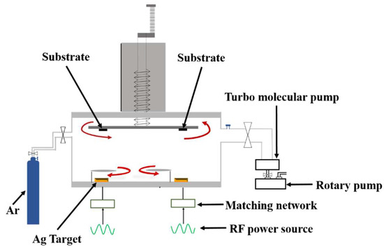
Figure 1.
Schematic diagram of the RF PMS system.
The structure of the chamber used for the film growth is presented in Figure 1. There are four target sites in the chamber, where all four targets can simultaneously be placed into the chamber for multilayer deposition. The upper substrate can be rotated 360°, and the four sets of samples can be fixed to the upper substrates. Furthermore, the chamber is connected to multiple air channels, where gases such as Ar, N2, and O2 can be introduced according to the requirements. The power supply of the device is composed of one DC power supply and two RF power supplies, which can be used to sputter various solid target materials including metals, insulators, and ferromagnetic materials. The vacuum of the equipment can be pumped to pressure values below 1 × 10⁻⁵ Pa. Only the Ag target, with a power of 600 W and an RF power supply of 13.56 MHz, was used in this experiment.
The coating process required simple adjustments to the input power and the gas flow rate. Six Ag nanofilm samples were prepared on Si substrates by adjusting the RF power, while keeping the chamber pressure at a constant value. The RF powers used were 20 W, 40 W, 60 W, 80 W, 100 W, and 160 W, whereas the sputtering time was 10 min and the working pressure was around 5 Pa, labeled as the first data set. The active gas was pure Ar (99.99%). No further heating was provided during the sputtering process. The second data set was obtained at an RF power of 100 W, in which Ag film was sputtered onto different substrates (Cu, Si, and Ti) for 10 min. The third data set was acquired by depositing Ag film on the Cu substrates, with a sputtering RF power of 100 W, but with varying sputtering times of 5 min, 10 min, and 15 min.
The surface morphology and the thickness of the samples were characterized using scanning electron microscopy (SEM, Hitachi SU-8010, Hitachi, Japan). The 3D morphology and RMS surface roughness of the films were obtained using atomic force microscopy (AFM, Dimension Icon, Bruker, Germany). The crystalline planar structures of the prepared Ag film were identified using X-ray diffraction (XRD, Bruker D8 ADVANCE, Bruker, Germany) with CuKα as the radiation source. Optical emission spectroscopy (OES, MS5204i, SOL Company, Belarus) was employed to study the different Ag-based species formed in the RF magnetron plasma. A passively compensated Langmuir probe (0601 ESPION, Hiden Analytical, United Kingdom) was positioned 50 mm directly above the Ag target for measurement of the RF magnetron plasma parameters (including plasma density, ne, and effective electron temperature, Te).
3. Results
3.1. Grain Size and Morphologies of Ag Film
The obtained XRD diffraction patterns for the Ag film are provided in Figure 2. The diffraction peaks of the Ag film were found at 2θ values of 39.6°, 46.4°, and 67.8°, corresponding to the planes Ag (111), Ag (200), and Ag (220) [16,17,18,19], respectively. It is noteworthy that a slight shift of the Ag (111) peak position was observed in this study. A similar phenomenon has also been reported for Ag films on TiN substrates [11], which may be attributed to stress states and lattice mismatch. Lattice parameter a for the Ag film was calculated from the Ag (220) peak using the Scherrer equation. The calculated values for a ranged from 4.041 Å to 4.112 Å, which are in good agreement with the bulk Ag lattice parameter of 4.086 Å, with slight deviations likely due to residual stress and the early coalescence of Ag grains. This is consistent with previous reports on the sputtering of Ag films on different substrates. As shown in Figure 2a, these three peaks can clearly be observed in the data obtained for the Si and Cu substrates, taken at the same deposition time and power of 5 min and 100 W, respectively. However, since the Si substrate peak was so intense, the Ag (220) diffraction peak was not clearly observable. The diffraction peak corresponding to the Ag (220) plane on the Si substrate was found to be weaker than for the Cu substrate. This suggests that better lattice matching between Ag and Cu promotes higher film crystallinity. The relatively low intensity of the Ag (220) peak on the Si substrate suggests the presence of a preferential (111) orientation in the Ag films. This is consistent with previous studies that have shown a strong (111) fiber texture in Ag films deposited on substrates such as Si, likely due to the lattice mismatch and the resulting strain in the early stages of film growth.
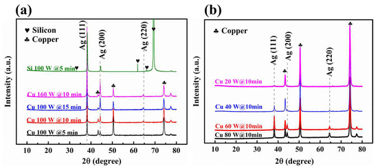
Figure 2.
(a) XRD of Ag film deposited on Si and Cu substrates (100W @ 5 min) and on Cu substrates at different times, and (b) XRD of Ag film deposited on Cu substrates at different RF powers.
In addition, according to Figure 2a,b, the peak position did not seem to shift too much with an increase in sputtering time or the RF power. For the Cu substrate, the diffraction peak corresponding to Ag (111) indicated that the Ag layer grew in a textured form [20,21]. On the Cu substrates, the intensity of the predominant peak attributed to the Ag (111) plane increased with an increase in deposition time and power. This phenomenon can be attributed to the formation of larger grains.
The average size of the Ag film was calculated from the Ag (220) peak using Scherrer’s formula, which is provided in Table 1. The plot of the change in grain size in relation to the sputtering power is provided in Figure 3. As seen from the fitting curve (red line), as the RF power increased from 20 W to 160 W, the coherent scattering region (CSR) size, calculated using the Scherrer formula, decreased from 30 nm to 2.5 nm, indicating a higher degree of crystallinity. However, the surface grain size observed in the SEM images increased with higher RF power, consistent with the larger atomic flux and enhanced adatom mobility at higher power. This may be attributed to the enhanced ion bombardment effect at higher RF power, which increases the nucleation rate while restricting grain growth. Previous studies have reported similar trends in the reduction of CSR size with increased RF power, which is linked to enhanced ion bombardment and improved adatom mobility during the sputtering process [22]. According to Table 1, the grain size also increased with the increase in the deposition time. At the initial deposition stage, many nucleation centers were generated on the substrate. Small crystals break into even smaller ones for a shorter deposition time period. As the sputtering time increased from 5 min to 15 min, the grain size grew from 6.19 nm to 7.18 nm, which is consistent with the grain growth model where nuclei gradually coalesce after initial nucleation.

Table 1.
The half-height width and grain size of Ag (220) peak as a function of sputtering time.
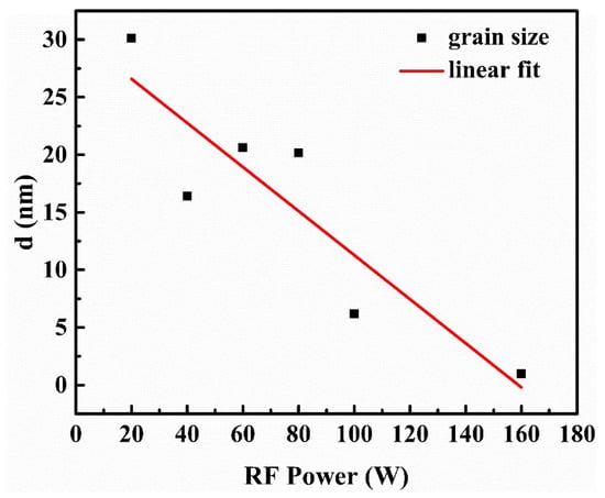
Figure 3.
Change trend of grain size with increasing RF power.
The change in surface morphology of the Ag film deposited on Si substrates with different sputtering times is shown in Figure 4, whereas the corresponding cross-section morphology is presented in the upper right corner of the figure. It can be seen in Figure 4a–c that the film thickness increased with the increase in the sputtering time, whereas the thickness ranged from 220 nm to 1130 nm at the selected sputtering power. However, as the sputtering time increased, the size of individual Ag grains increased, as observed in the SEM images, due to the coalescence of smaller grains into larger ones. This increase in grain size corresponds to the enhanced adatom mobility and nucleation rate at higher RF power and longer sputtering time. This can be attributed to the fact that the thickness of Ag film increased with an increase in the sputtering time. However, with continued film growth, the sputtered Ag film then effectively formed a thick Ag film, which acted as a Ag substrate on which further deposition continued. This indicated that substrates with different thermal conductivities affected the reaction rates and, hence, further migration of adsorbed molecules on the surface. To confirm this hypothesis, thick Ag films were pre-deposited on different substrates in the subsequent experiments. The thickness increased approximately linearly with the sputtering time, and the slope of the red fit dotted line was calculated as 72.14 nm/min. The film thickness increased almost linearly with the RF power, while all other parameters were kept unchanged. The deposition rate of the film was calculated to be around 72.14 nm/min at an RF power of 100 W.
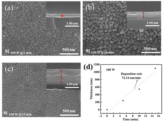
Figure 4.
(a–c) SEM of Ag film deposited on Si substrate changes with sputtering time; (d) variation trend of Ag film thickness with sputtering time, and deposition rate of thin films at RF power of 100 W fitted by red curve.
As shown in Figure 5a–e, both the particle size and growth rate of the Ag films increased with rising RF power from 20 W to 160 W under constant sputtering conditions (10 min, 5 Pa). The inset of Figure 5f presents the corresponding film thickness and calculated deposition rate as a function of RF power. A nearly linear increase in deposition rate is observed with increasing power, ranging from 3.7 nm/min to 89.19 nm/min. This trend is attributed to the enhanced kinetic energy of sputtered atoms at higher RF powers, which promotes greater atomic mobility, thereby accelerating nucleation and film growth.
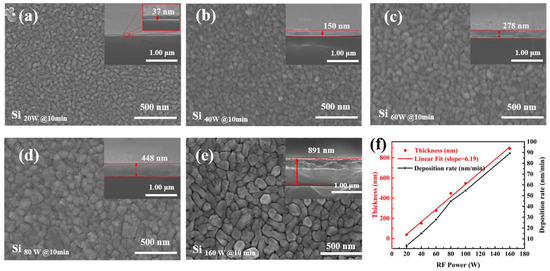
Figure 5.
(a–e) SEM of Ag film deposited on Si substrate changes with RF power; (f) growth height and deposition rate of Ag film change with RF power.
The SEM images of Ag film deposited on different substrates (Si, Cu, and Ti) under the same growth conditions are presented in Figure 6. The SEM results indicate that different substrates significantly influence the grain orientation and crystallinity of the films. Previous studies have shown that stress and lattice mismatch occur when Ag is deposited on Ti substrates [10] or TiN substrates [11], whereas on Cu substrates, the metallic seed layer helps to reduce the critical thickness for film continuity and improve electrical conductivity [12]. It can be seen from Figure 6 that the deposited particles of the Ag nano thin films grown on the Si substrate were smaller in size, and they exhibited a more uniform distribution in comparison to the Ag films grown on the Cu and Ti substrates. The particle size of the Ag nanofilm deposited on the Cu substrate was found to be slightly smaller than that for the Ti substrate. Therefore, the SEM images for the Ag film deposited on different substrates clearly showed that the substrate type influenced the morphology of the thin films. The difference in lattice parameters of various materials determine the lattice mismatch, the infiltrability, and the thermal expansion coefficients of the materials. The type of substrate material influences the deposition and growth processes of the thin films, as well as their microstructure. This may be linked to the fact that the crystal structure and thermal conductivity of the substrate has a direct effect on the morphology of the nanoparticles [18,23,24,25]. Hence, this explains why the size of the film particles decreased as sputtering time was increased, as shown in Figure 4. This was due to the fact that the deposited Ag film formed a thick Ag layer after a certain period of time after the start of the deposition. As deposition time increased further, the subsequent Ag film was actually being deposited onto a dense Ag film.

Figure 6.
SEM images of Ag film deposited on different substrates under the same sputtering conditions.
The AFM images obtained for the Ag film prepared at RF powers ranging from 20 W to 160 W with the same sputtering time (10 min) and pressure are provided in Figure 7a–f. In the observation area of 2 μm × 2 μm, it can be seen that the film as a whole was quite flat and compact. However, the root mean square (RMS) surface roughness of the films gradually increased with an increase in the RF power. The thickness of the Ag film was therefore closely related to the surface roughness of the prepared nanoparticles. Moreover, at increased RF powers, the high-energy particles bombarded the film surface, which led to an increase in the surface roughness. From Figure 7f, it can be seen that the film surface exhibited island-type characteristics, implying that high-energy particles were formed due to bombardment at increased RF powers.
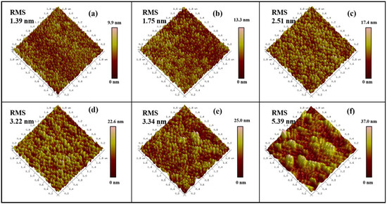
Figure 7.
(a–f) RMS of Ag film at RF powers of 20 W, 40 W, 60 W, 80 W, 100 W, and 160 W, respectively.
3.2. Diagnosis of RF-PMS
The obtained characteristic optical emission spectra (OESs) of the discharge plasma with a fixed RF frequency of 13.56 MHz and at different RF powers of 60 W, 80 W, 100 W, and 120 W are presented in Figure 8. The working pressure was 5 Pa. The OES results revealed optical peaks of atoms and ions of Ag and Ar. All emission spectra exhibited two strong Ag resonance emission lines at 328.1 nm and 338.3 nm, corresponding to excitation energies (Eex) of 3.78 eV and 3.66 eV, respectively. The OES shows that the intensity of the main emission lines of Ag atoms at 328.1 nm and 338.3 nm increases with RF power, indicating a higher density of excited Ag atoms at elevated power levels. There were weak Ag emission lines at 421.1 nm, 520.9 nm, 546.6 nm, and 547.2 nm, which corresponded to different transitions from the energy band between Eex = 6.04–6.72 eV to the energy band between Eex = 3.66–3.78 eV. These were used to determine the ionization potential of Ag to be 7.574 eV. The Ag+ emission line at 349.5 nm corresponded to the transition from 4d85s2 (13.53–14.08 eV) to 4d95p (10.19–11.14 eV). The Ag+ emission peak at 349.5 nm was relatively weak compared to the dominant Ag atomic lines at 328.1 nm and 338.3 nm (3.78 eV and 3.66 eV) [26].
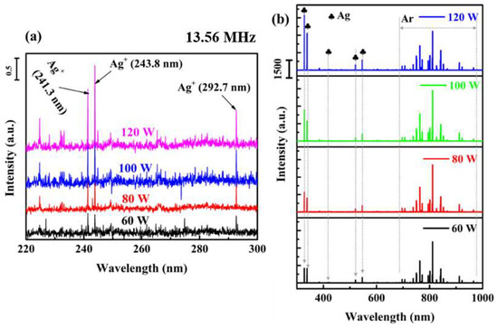
Figure 8.
Characteristic OES of RF magnetron discharge plasmas with an RF power of 60 W, 80 W, 100 W, and 120 W, as well as an RF frequency of 13.56 MHz; (a) wavelength range of 220–300 nm and (b) 300–1000 nm.
The spectral lines of Ag at 520.9 nm and at 243.8 nm were used to establish a correlation between the RF magnetron plasma and the RF power. These lines were specifically chosen as their peaks did not overlap with any other spectral lines. The results revealed that the intensity of these emission lines increased with the increase in the RF power.
The formed RF-PMS plasma was tested using a Langmuir probe device. The variation in the values of Te and ne as a function of the RF power was measured using the Langmuir probe at a discharge pressure of about 5.0 Pa and at an Ar flow rate of 50 sccm. The results of this test are presented in Figure 9.
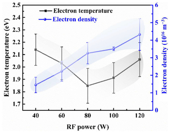
Figure 9.
Variation trend in electron temperature and electron density with RF power.
It can be observed that the value of Te decreased initially and then increased in relation to the RF power. As the RF power was increased from 40 W to 80 W, the number of Ag atoms at the sputtering site from the Ag target increased. In addition, the frequency of inelastic collisions between the electrons and the Ag atoms, as well as the loss in energy also increased within this range of RF power, while the electron temperature dropped rapidly as the RF power was increased from 40 W to 80 W. The electron density increased with the increase in the RF power. The increase in RF power provided the incoming particles with enough energy to break the chemical bonds in the target and ionize the atoms. Atoms present on the surface of the Ag target are the primary particles that collide and, hence, transfer their energy to other atoms within the target to produce a large amount of energy. The secondary particles then, in turn, collide with other atoms in the target, thereby transferring their energy to them, thus forming an atomic recoil cascade along the path of the incident ions. The bombardment of high-energy electrons, Ar+ ions, and Ar neutral species on the surface of the Ag target leads to the emission of secondary electrons. These electrons play a key role in the MS discharge process. At increased RF powers, secondary electrons are emitted from the cathode and sputtered Ag atoms are diffused into the plasma. The frequency of inelastic collisions between the electrons and the atoms increases, thus ionizing more atoms into ions. The density of electrons increased with the increase in the RF power. For the plasma to be electrically neutral on a macroscopic level, the ion density must also increase with the increase in RF power. As ion density is closely related to the film growth process, it also explains why the thickness of the Ag nanoparticle films increased with the increase in the RF power. The ionization of sputtered atoms increased as the thin film was deposited. This was beneficial for controlling the direction of the formed ions, resulting in the growth of higher-quality thin films.
4. Discussion
The crystal orientation, thickness, grain size, and morphology of Ag film changed with the increasing RF power. Thus, the plasma parameters, such as RF power, have a significant effect on the microstructures of Ag film. It can be speculated that the change in the microstructures of Ag film was related to the process of generation, transport, and deposition of the sputtered particles. A schematic diagram of Ag film sputtering, transport, and deposition in low-RF power and high-RF power is presented, respectively, in Figure 10. During the complicated deposition process of Ag film, the discharge is maintained by sputtering gas. In pure Ar discharge, Ar+ ions provide the main source of ions, while Ar atoms also exist in the vacuum, as confirmed by the plasma OES diagnostic techniques described in Section 3.2. The electron density in high-RF power are higher than those in low-RF power under the same parameters, as shown in Figure 9. A large quantity of sputtered Ar+ results in high sputter yields in high-RF power, so bigger and more numerous Ag clusters exist in high-RF power compared with in low-RF power. Another reason is that the RF power affects the transport and collision process of the sputtered particles, resulting in the change in energy.
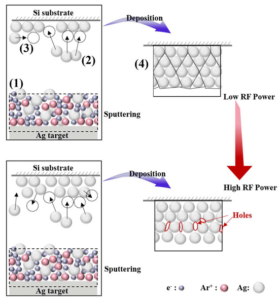
Figure 10.
Schematic representation of the RF magnetron sputtering process: (1) sputtering of Ag atoms from the target, (2) gas-phase collisions and thermalization of sputtered atoms, (3) surface adsorption and diffusion of atoms on the substrate, and (4) island formation and coalescence to form a continuous Ag film.
Due to migration and diffusion, Ag clusters can move to the gap between clusters, which leads to the close-packed growth of Ag clusters in the deposition process. Ag clusters have higher energy at higher RF power. Clusters with low mobility and diffusivity tend to remain in their initial position after deposition on Si substrates; therefore, under the condition of low-RF power discharge, Ag clusters have relatively loose growth patterns, as proven by the SEM images in Figure 5. Furthermore, in high-RF power discharge, the large size and high mobility of Ag clusters lead to the initial large size in the coalescence stage. During grain growth, lower mobility and diffusion leads to a higher nucleation rate in low-RF power discharge. Therefore, the grain size increases with the increase in the discharged RF power. The relatively higher strain energy that exists in Ag film is due to the large number of defects that exist in loose-packed patterns of Ag clusters [14]. In summary, RF power significantly influences the microstructure and strain energy of the Ag film.
The growth of Ag follows a pattern of islanding, coalescence, and continuous film formation. Higher RF power increases the arriving flux and enhances adatom mobility, shortening the time to percolation and favoring stronger texture. Ion-assisted effects can refine CSR while enlarging surface grains, explaining the occasional differences between Scherrer CSR and SEM grain size. Compared with DC sputtering and HiPIMS reports, our RF-MS results clarify how electron density/temperature (diagnosed by OES/Langmuir) relate to Ag texture and continuity under combined variations of power, time, and substrate. This diagnostic-coupled view provides actionable guidance beyond single-parameter studies.
The electrical properties of Ag thin films are closely related to the morphology of their nanoparticles. During the study, the I–V characteristics of the samples were measured using a semiconductor analyzer with a two-probe method, as shown in Figure 11. Figure 11 displays the I–V curves of Ag films prepared under different deposition conditions, with the inset showing the calculated resistance values. All curves exhibit good linearity, indicating typical Ohmic behavior in the low-voltage region and stable metallic conductivity. The inset at the lower right corner further quantifies the variation trend of the sheet resistance among different samples.
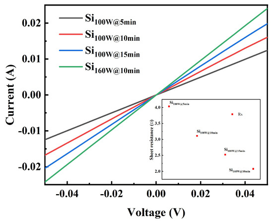
Figure 11.
Two-probe I–V curves of Ag films under different deposition conditions, showing linear Ohmic behavior; inset: resistance comparison.
With variations in sputtering power and time, the electrical conductivity of the films changes significantly. When the deposition time is fixed at 10 min, increasing the sputtering power from 100 W to 160 W results in a noticeable increase in the slope of the I–V curve, indicating a decrease in film resistance from 3.1 Ω to 2 Ω. This is attributed to the higher atomic flux density and faster deposition rate at higher power, which leads to denser films and larger grain sizes, thereby reducing electron scattering and enhancing electron mobility.
When the power is fixed at 100 W, extending the deposition time from 5 min to 15 min also results in an increased slope of the I–V curve. A longer deposition time produces thicker and more continuous films, facilitating the formation of complete conductive pathways and thus reducing the resistance from 4 Ω to 2.5 Ω. The development of low-cost fabrication methods for Ag films with low resistivity and high conductivity highlights their great potential in microelectronic applications.
The electrical measurements were performed using a two-probe method to obtain the I–V characteristics. Although the two-probe method can introduce contact resistance, the measurements were conducted within the low-voltage region where Ohmic behavior was observed, minimizing the impact of contact resistance on the results. Future studies will incorporate the four-probe method to eliminate contact resistance effects and provide more accurate data on sheet resistance and conductivity.
5. Conclusions
This study systematically explores the influence of key RF magnetron sputtering parameters—including RF power, deposition time, and substrate material—on the plasma characteristics and nanostructure of Ag thin films. Compared with previous studies that focused only on a single process parameter, this work systematically investigates, for the first time, the synergistic effects of RF power, sputtering time, and substrate type. By combining OES and Langmuir probe diagnostics, a direct correlation between plasma parameters and film structure evolution has been established. The results demonstrate that increasing RF power significantly enhances plasma excitation, leading to higher electron density and intensified ion bombardment, which, in turn, promotes finer grain size, better crystallinity, and faster deposition rates. Deposition time primarily affects film thickness and grain coalescence behavior, while substrate type modulates the film’s crystalline orientation and morphology due to differences in lattice matching and thermal conductivity.
Through combined diagnostics using OESs and Langmuir probing, a direct correlation is established between plasma parameters and film structure. The electrical performance of the films is closely tied to their microstructure, with denser, well-crystallized films exhibiting lower resistance. These findings not only deepen our understanding of sputtering-driven film growth mechanisms under variable plasma conditions, but also provide practical guidance for tailoring Ag film properties for applications in plasmonic sensors, catalysis, and flexible electronics.
We recognize that RF magnetron sputtering (RF-MS) offers advantages in terms of film uniformity and purity compared to DC sputtering, but the grain growth mechanisms and electrical properties observed in this study would benefit from comparison with alternative sputtering methods, such as HiPIMS, which can offer enhanced ionization and energy control. Future work will include the statistical analysis of experimental replication and comparisons with other sputtering techniques to provide a more comprehensive understanding of the effects of deposition methods on Ag thin films.
Author Contributions
Conceptualization, P.J. and X.W.; methodology, J.C.; software, T.H.; validation, J.C., Y.W. and T.H.; formal analysis, J.C.; investigation, J.C.; resources, Y.W.; data curation, J.C.; writing—original draft preparation, J.C.; writing—review and editing, P.J. and X.W.; visualization, T.H.; supervision, P.J. and X.W.; project administration, P.J.; funding acquisition, Y.W. and X.W. All authors have read and agreed to the published version of the manuscript.
Funding
This work was supported by the National Natural Science Foundation of China (No. 12175160, 12305284); the University–Industry Collaborative Education Program of the Ministry of Education (230706093253200); the Suzhou Basic Research Project (SJC2023003); Suzhou City University National-level Project Preliminary ResearchTopic (2023SGY011); and the Natural Science Foundation of the Jiangsu Higher Education Institutions of China (24KJB140016).
Institutional Review Board Statement
Not applicable.
Informed Consent Statement
Not applicable.
Data Availability Statement
The data presented in this study are available on request from the corresponding author.
Acknowledgments
The authors would like to acknowledge the technical assistance provided by the laboratory staff in material characterization and plasma diagnostics. The authors have reviewed and edited the output and take full responsibility for the content of this publication.
Conflicts of Interest
The authors declare no conflicts of interest.
References
- Yan, L.; Yan, Y.; Xu, L.; Ma, R.; Jiang, F.; Xu, X. Large Range Localized Surface Plasmon Resonance of Ag Nanoparticles Films Dependent of Surface Morphology. Appl. Surf. Sci. 2016, 367, 563–568. [Google Scholar] [CrossRef]
- Silver-Based Plasmonic Nanoparticles for and Their Use in Biosensing. Available online: https://www.mdpi.com/2079-6374/9/2/78 (accessed on 20 August 2025).
- Jamnig, A.; Pliatsikas, N.; Konpan, M.; Lu, J.; Kehagias, T.; Kotanidis, A.N.; Kalfagiannis, N.; Bellas, D.V.; Lidorikis, E.; Kovac, J.; et al. 3D-to-2D Morphology Manipulation of Sputter-Deposited Nanoscale Silver Films on Weakly Interacting Substrates via Selective Nitrogen Deployment for Multifunctional Metal Contacts. ACS Appl. Nano Mater. 2020, 3, 4728–4738. [Google Scholar] [CrossRef]
- Filip, A.V.; Sava, B.A.; Medianu, R.V.; Boroica, L.; Dinca, M.C.; Pascu, R.; Tigau, N.; Andrei, A.; Moldovan, A.; Dumitru, M.; et al. Ultrathin Films of Silver by Magnetron Sputtering. Inorganics 2022, 10, 235. [Google Scholar] [CrossRef]
- Campos, C.; Herguedas, N.; Carretero, E. Optimizing Sputter Deposition Conditions of Silver Thin Films Used in Low-Emissivity Coatings in an In-Line Deposition System. Coatings 2023, 13, 1556. [Google Scholar] [CrossRef]
- Reck, K.A.; Bulut, Y.; Xu, Z.; Liang, S.; Strunskus, T.; Sochor, B.; Gerdes, H.; Bandorf, R.; Müller-Buschbaum, P.; Roth, S.V.; et al. Early-Stage Silver Growth during Sputter Deposition on SiO2 and Polystyrene Comparison of Biased DC Magnetron Sputtering, High-Power Impulse Magnetron Sputtering (HiPIMS) and Bipolar HiPIMS. Appl. Surf. Sci. 2024, 666, 160392. [Google Scholar] [CrossRef]
- Mao, L.; Geng, Y.; Cao, Y.; Yan, Y. Uniform High-Reflectivity Silver Film Deposited by Planar Magnetron Sputtering. Vacuum 2021, 185, 109999. [Google Scholar] [CrossRef]
- Park, H.K.; Yoon, J.K.; Kim, K. Novel Fabrication of Ag Thin Film on Glass for Efficient Surface-Enhanced Raman Scattering. Langmuir 2006, 22, 1626–1629. [Google Scholar] [CrossRef]
- Lu, D.; Yang, J.; Wang, X.; Gao, S.; Li, M.; Ji, H. Effect of Sputtering Power on the Microstructure and Properties of Silver Films Prepared by Magnetron Sputtering. Mater. Today Commun. 2025, 42, 111288. [Google Scholar] [CrossRef]
- Xu, Y.; Zhang, J.; Liang, F.; Yin, M.; He, M. Investigation of Magnetron Sputtered Nano-Silver Coating on Titanium Surface with Micro-Nanostructure. Surf. Interfaces 2023, 38, 102770. [Google Scholar] [CrossRef]
- De Arruda, A.C.S.; Mansano, R.D.; Ordonez, N.; Ruas, R.; Durrant, S.F. Ag Behavior on TiN Thin Films for Decorative Coatings. Coatings 2024, 14, 322. [Google Scholar] [CrossRef]
- Guan, M.; Wang, L.; Zhang, Y.; Wang, D.; Wang, Q.; Liu, J. Effect of Metal Seed Layer on the Critical Thickness and Photoelectric Properties of Ultrathin Ag Films. Mater. Today Commun. 2023, 37, 107540. Available online: https://www.sciencedirect.com/science/article/abs/pii/S2352492823022316 (accessed on 20 August 2025). [CrossRef]
- Ma, D.; Ji, M.; Yi, H.; Wang, Q.; Fan, F.; Feng, B.; Zheng, M.; Chen, Y.; Duan, H. Pushing the Thinness Limit of Silver Films for Flexible Optoelectronic Devices via Ion-Beam Thinning-Back Process. Nat. Commun. 2024, 15, 2248. [Google Scholar] [CrossRef] [PubMed]
- Metawa, A.E.; El-Hossary, F.M.; Raaif, M.; SalahEl-Deen, M.; El-Moula, A.A.A. Langmuir Probe and Optical Emission Spectroscopy Studies for RF Magnetron Sputtering during TiON Thin Film Deposition. Chin. J. Phys. 2020, 68, 168–177. [Google Scholar] [CrossRef]
- Makówka, M.; Sobczyk-Guzenda, A.; Pawlak, W.; Wendler, B.; Gazicki-Lipman, M.; Szymanowski, H. Correlation between Plasma Parameters and Structure of Thin TiO2 Films Deposited by Conventional and Pulsed Magnetron Sputtering Methods. Appl. Surf. Sci. 2022, 578, 151808. [Google Scholar] [CrossRef]
- Kim, W.M.; Ku, D.Y.; Lee, K.S.; Cheong, B. Effect of Oxygen Content and Deposition Temperature on the Characteristics of Thin Silver Films Deposited by Magnetron Sputtering. Appl. Surf. Sci. 2010, 257, 1331–1336. [Google Scholar] [CrossRef]
- Formica, N.; Ghosh, D.S.; Carrilero, A.; Chen, T.L.; Simpson, R.E.; Pruneri, V. Ultrastable and Atomically Smooth Ultrathin Silver Films Grown on a Copper Seed Layer. ACS Appl. Mater. Interfaces 2013, 5, 3048–3053. [Google Scholar] [CrossRef]
- Mashaiekhy, J.; Shafieizadeh, Z.; Nahidi, H. Effect of Substrate Temperature and Film Thickness on the Characteristics of Silver Thin Films Deposited by DC Magnetron Sputtering. Eur. Phys. J. Appl. Phys. 2012, 60, 20301. [Google Scholar] [CrossRef]
- Maréchal, N.; Quesnel, E.; Pauleau, Y. Silver Thin Films Deposited by Magnetron Sputtering. Thin Solid Film. 1994, 241, 34–38. [Google Scholar] [CrossRef]
- Schmidl, G.; Dellith, J.; Kessler, E.; Schinkel, U. The Influence of Deposition Parameters on Ti/Pt Film Growth by Confocal Sputtering and the Temperature Dependent Resistance Behavior Using SiOx and Al2O3 Substrates. Appl. Surf. Sci. 2014, 313, 267–275. [Google Scholar] [CrossRef]
- Hu, Y.; Zhu, J.; Zhang, C.; Yang, W.; Fu, L.; Li, D.; Zhou, L. Understanding the Preferred Crystal Orientation of Sputtered Silver in Ar/N2 Atmosphere: A Microstructure Investigation. Adv. Mater. Sci. Eng. 2019, 2019, 3079393. Available online: https://onlinelibrary.wiley.com/doi/10.1155/2019/3079393 (accessed on 20 August 2025). [CrossRef]
- Jeon, D.Y. Influence of Dc Magnetron Sputtering Parameters on Surface Morphology of Indium Tin Oxide Thin Films. Appl. Surf. Sci. 2004, 221, 136–142. [Google Scholar] [CrossRef]
- Gao, X.; Hu, M.; Fu, Y.; Weng, L.; Liu, W.; Sun, J. Low Temperature Deposited Ag Films Exhibiting Highly Preferred Orientations. Mater. Lett. 2018, 213, 178–180. [Google Scholar] [CrossRef]
- Dong, L.; Srolovitz, D.J. Texture Development Mechanisms in Ion Beam Assisted Deposition. J. Appl. Phys. 1998, 84, 5261–5269. [Google Scholar] [CrossRef]
- Jung, Y.S. Study on Texture Evolution and Properties of Silver Thin Films Prepared by Sputtering Deposition. Appl. Surf. Sci. 2004, 221, 281–287. [Google Scholar] [CrossRef]
- Gardonio, S.; Karolak, M.; Wehling, T.O.; Petaccia, L.; Lizzit, S.; Goldoni, A.; Lichtenstein, A.I.; Carbone, C. Excitation Spectra of Transition-Metal Atoms on the Ag (100) Surface Controlled by Hund’s Exchange. Phys. Rev. Lett. 2013, 110, 186404. [Google Scholar] [CrossRef]
Disclaimer/Publisher’s Note: The statements, opinions and data contained in all publications are solely those of the individual author(s) and contributor(s) and not of MDPI and/or the editor(s). MDPI and/or the editor(s) disclaim responsibility for any injury to people or property resulting from any ideas, methods, instructions or products referred to in the content. |
© 2025 by the authors. Licensee MDPI, Basel, Switzerland. This article is an open access article distributed under the terms and conditions of the Creative Commons Attribution (CC BY) license (https://creativecommons.org/licenses/by/4.0/).