Article

Electrodeposition of Metallic Tungsten Coating on 9Cr-ODS Steel Substrate from Binary Oxide Molten Salt

by
Xiaoxu Dong
,
Yusha Li
,
Yajie You
,
Zeyu Gao
and
Yingchun Zhang
*
School of Materials Science and Engineering, University of Science and Technology Beijing, 30 Xueyuan Road, Haidian District, Beijing 100083, China
*
Author to whom correspondence should be addressed.
These authors contributed equally to this work.
Coatings 2025, 15(3), 257; https://doi.org/10.3390/coatings15030257
Submission received: 2 January 2025 / Revised: 17 February 2025 / Accepted: 19 February 2025 / Published: 21 February 2025

Abstract

:
Characteristics of electrodeposited tungsten coatings prepared at 1193 K and varying current density were investigated. The crystal structure and microstructure of tungsten coatings were characterized by scanning electron microscopy (SEM), X-ray diffraction (XRD), and photoelectron spectroscopy (XPS). The results indicated that pulsed current density significantly influence the tungsten nucleation and electro-crystallization phenomena. The average grain size of the coating becomes larger with increasing current density, which demonstrates that appropriate high cathodic current density can accelerate the growth of grains on the surface of the substrate. The micro-hardness of tungsten coatings increases with increasing thickness and then slightly decreases; the maximum micro-hardness is 589.55 HV, with the oxygen content remaining below 0.03 wt%.

1. Introduction

The technological realization of the fusion power source is critically dependent on the successful development of high-performance materials. These materials will have to be operated in extreme conditions, being subjected to complex thermal, mechanical, and chemical loads as well as strong irradiation. Tungsten is widely applied in the nuclear industries due to its high melting point (3695 K), low vapor pressure (p = 1.3 × 10⁻⁷ Pa), high thermal conductivity, low particle sputtering yield, and tritium retention [1,2,3]. However, tungsten is difficult to machine and weld; a possible solution for the utilization of tungsten at plasma facing surfaces is to coat the structural or heat sink material with a tungsten layer, which has been used as a heat sink coating for plasma oriented material (PFM). Among all the methods for realizing effective joints between tungsten armors and steel substrates, the deposition of tungsten coatings on substrates is efficient and economical [4,5,6]. It can be directly used for modular in situ replacement on the substrate.
Tungsten coatings can be obtained using multiple processes [7,8]. Techniques for obtaining high quality coatings, including vacuum plasma spray (VPS), physical vapor deposition (PVD), and chemical vapor deposition (CVD) have been investigated over recent decades [9,10]. But the disadvantages of the tungsten coatings prepared by normal spraying methods are obvious: weak bonding strength, high porosity, and inevitably introduced impurities. Fortunately, electrodeposition as a niche technology should have the potential to overcome these drawbacks [11]. Electrodeposition is one of the promising alternatives to fabricate functional tungsten coatings due to its simple, efficient process and because of its potential to cover complex extended surfaces at low cost.
In our prior research, we successfully achieved high-quality tungsten coatings with strong adhesion to copper alloy substrates through molten salt electrodeposition. However, a large body of literature shows that the combination of steel and tungsten is problematic [12,13], and the tungsten coating obtained by molten salt electrodeposition is expected to solve the problem of the problematic combination of steel and tungsten. Furthermore, based on our previous findings, coatings prepared by pulsed current electrodeposition are smoother compared to those obtained by direct current. Therefore, this study aims to develop tungsten coatings with enhanced adhesion to steel using pulsed current electrodeposition in molten salt.

2. Experiment and Parameters

2.1. Coating Deposition

All the chemicals were analytical reagent grade. Na2WO4−WO3 binary oxide molten salt was dried in a furnace at 473 K and 773 K, respectively, for 12 h. The dried chemicals were thoroughly mixed into a eutectic composition (Na2WO4:WO3 = 0.6:0.2, by mole ratio) in an alumina crucible, and then the crucible was set in an electric resistance furnace for electrodeposition. The heating rate of the mixed molten salt was 5 K/min. The working electrode was a 9Cr-ODS steel plate (C: 0.1 wt%, Cr: 9 wt%, W: 2 wt%, Mn: 0.5 wt%, Si: 0.15 wt%, V: 0.05 wt%, Ti: 0.05 wt%, Ta: 0.05 wt%, N: 0.05 wt%, O: 0.45 wt%, Y: 0.3 wt%, and Fe balance, 20 × 20 × 5 mm). The counter electrode was a tungsten plate (99.95%, 30 × 30 × 5 mm). The surfaces of electrodes were polished by mechanical and chemical methods to obtain high quality surfaces. The temperature was set as 1173 K. The average current density was set from 10 mA/cm2 to 70 mA/cm2. The frequency, duty cycle, and deposition duration were set as 1000 Hz, 30%, and 1 h, respectively.

2.2. Coating Characterization

The surface and cross-sectional morphology of the coated samples were observed by scanning electron microscopy (SEM, JSM6480LV) with elemental analysis. The phase and crystal orientation of W coatings were detected by X-ray diffraction (XRD, Rigaku Industrial Co., Ltd., Tokyo, Japan, D/MAX-BB). The oxidation state of tungsten in the coatings was characterized using X-ray photoelectron spectroscopy (XPS, Thermo Fisher Scientific Co., Ltd., Waltham, MA, USA, ESCALAB 250Xi). Micro-hardness of the coatings was measured by a EM1500L-6 micro hardness instrument with a loading force of 25 N and loading time of 10 s, and an average of five indentations was calculated. For the measurement of the oxygen content, the tungsten coating was separated from the 9Cr-ODS substrate by chemical dissolution in a dilute hydrochloric acid solution. The oxygen content was measured using a oxygen–nitrogen–hydrogen analyzer (Leco Co., Ltd., St Joseph, MI, USA, TCH600). The bonding strength was measured by tensile means, using a universal testing machine.

3. Results and Discussions

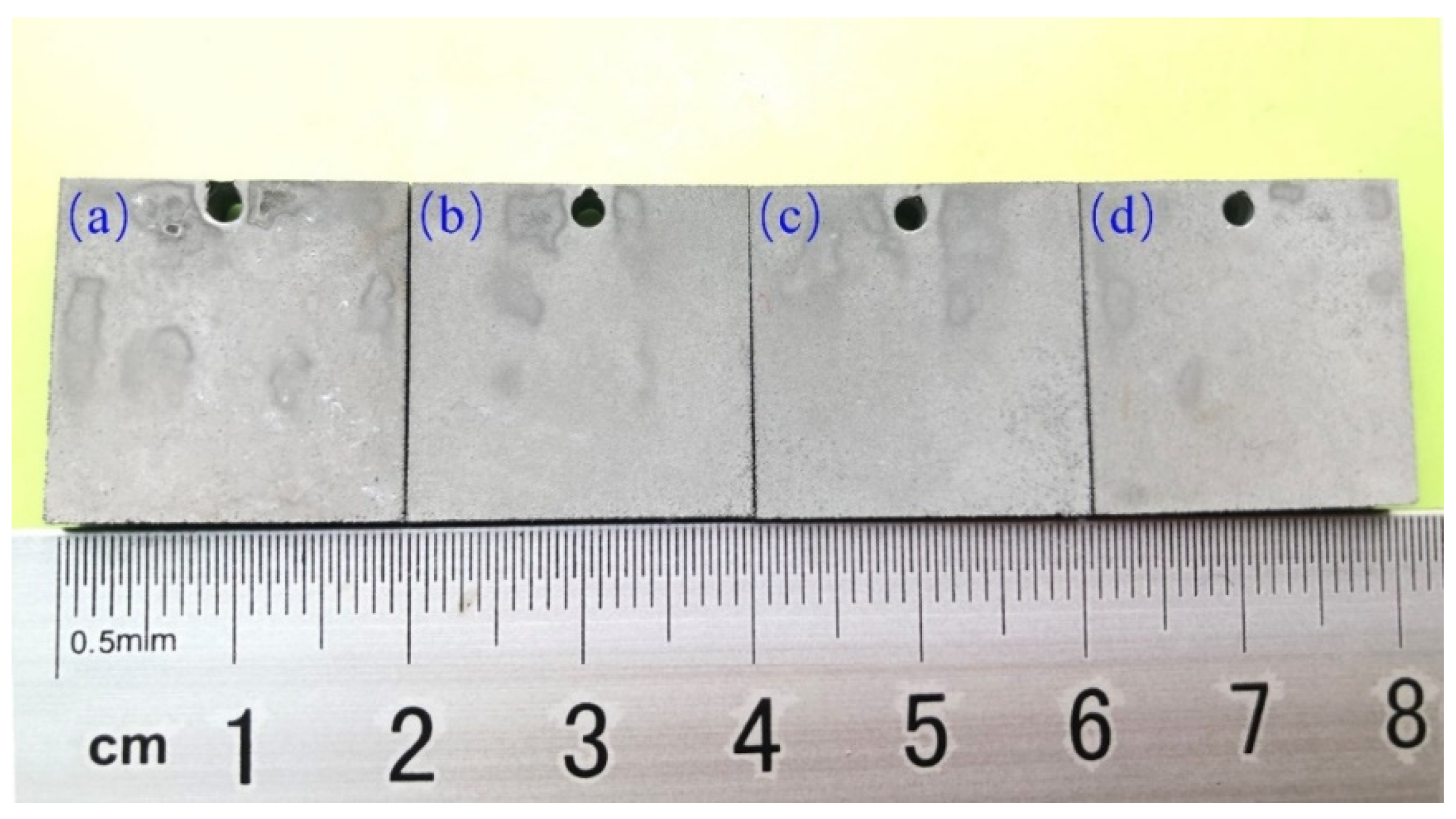
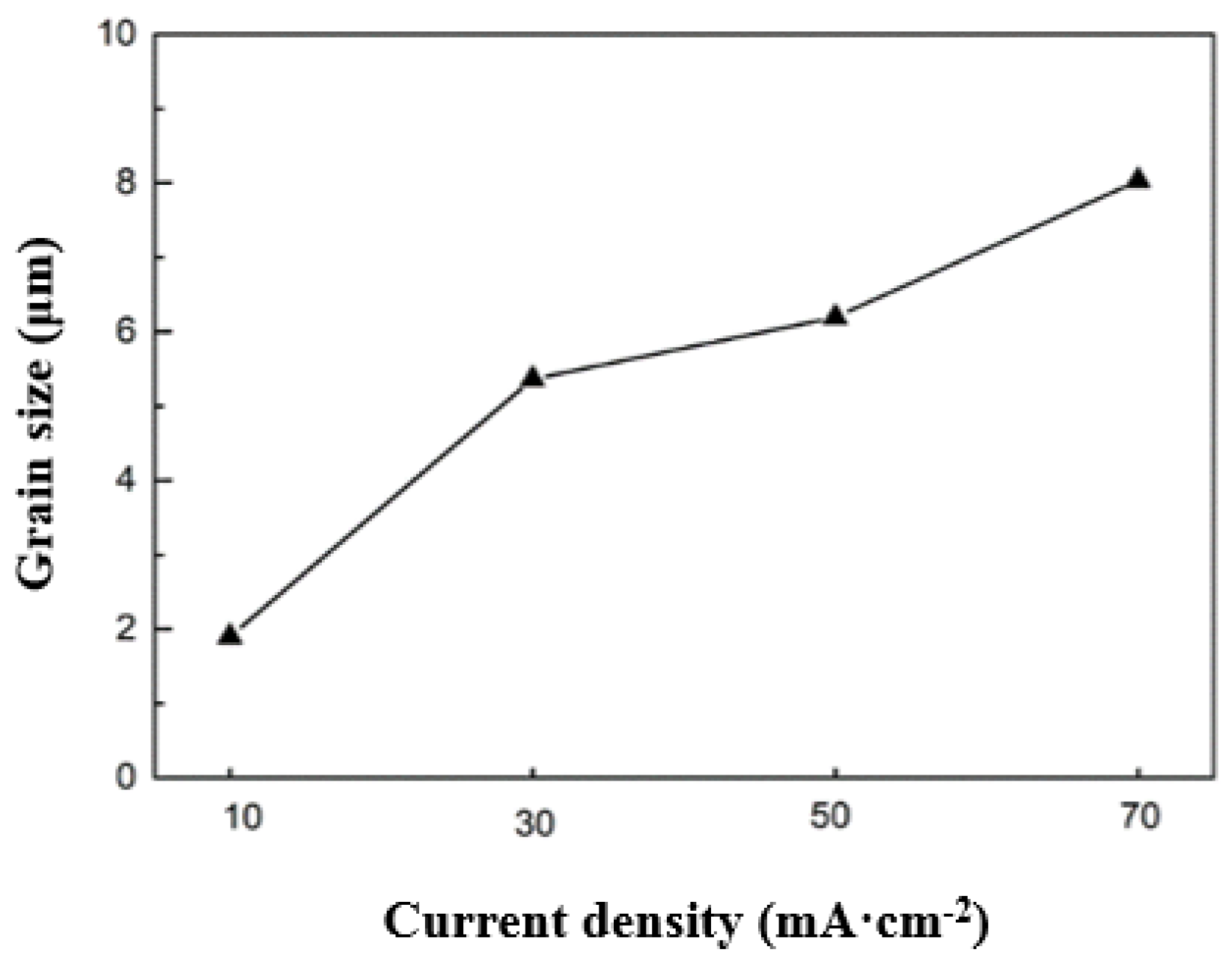
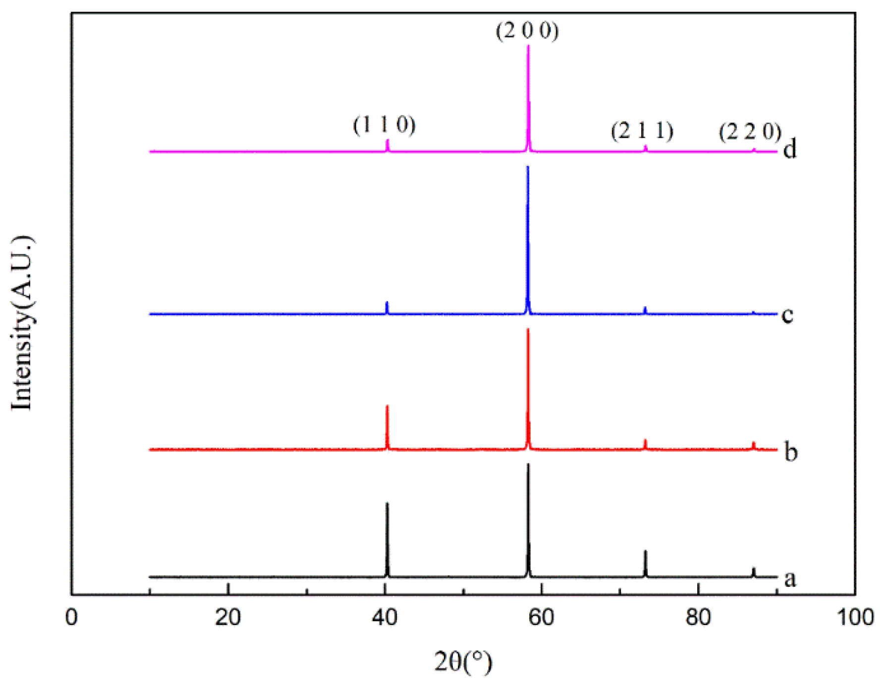
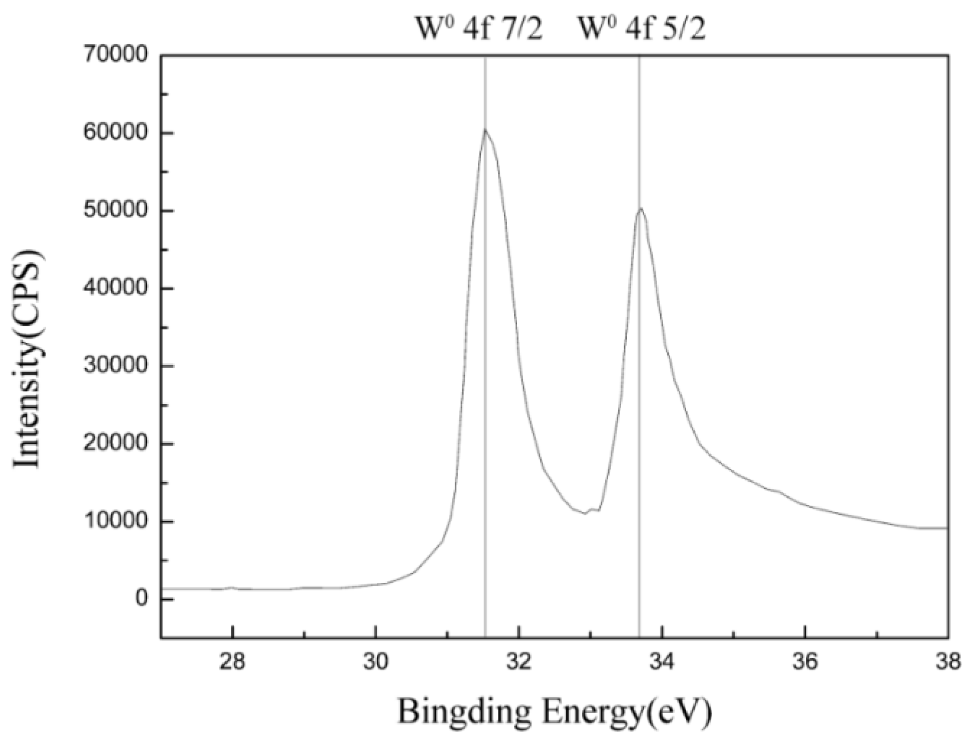
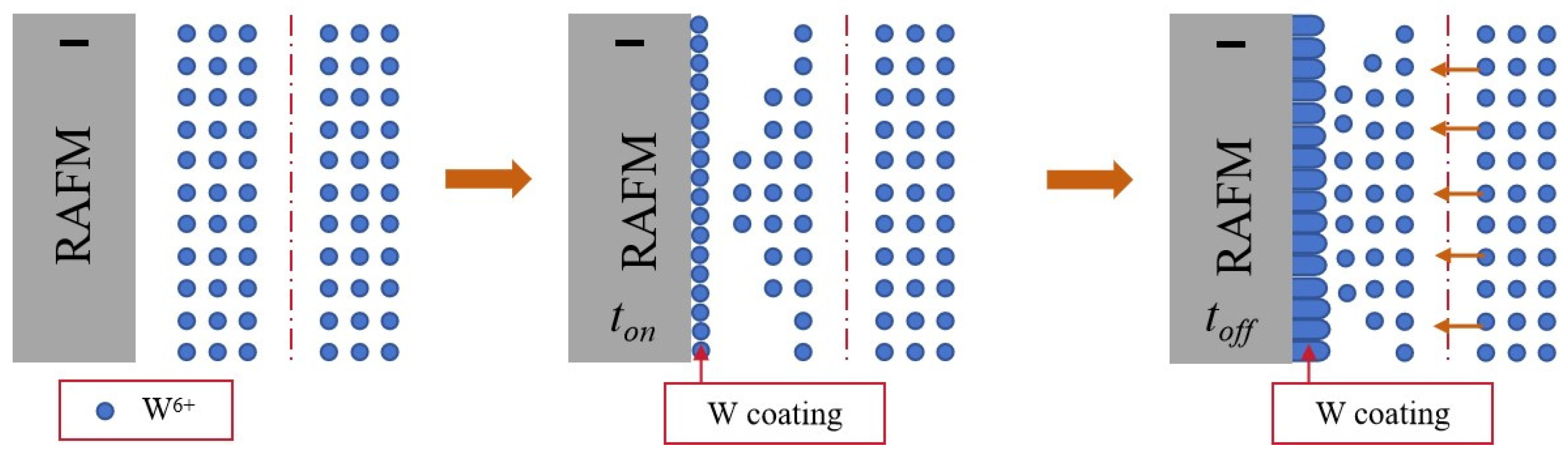
3.1. Microstructure and Crystal Structure of Thick Tungsten Coating

Figure 1 illustrates the macroscopic morphologies of tungsten coatings deposited at various pulse current densities. As depicted in the figure, silver-gray tungsten coatings can be successfully electrodeposited on the 9Cr-ODS steel substrate, exhibiting excellent coverage and a dense, smooth surface without visible cracks or pores. However, variations in macroscopic morphology are observed at different current densities. Specifically, when the current density exceeds 70 mA·cm−2, granular dendrites appear on the coating surface, which exhibit poor adhesion and tend to flake off during ultrasonic cleaning. In contrast, at current densities of 30 and 50 mA·cm−2, the coating surfaces are very smooth, with few protrusions.
The variations in the surface morphology of the tungsten coating can be further elucidated through corresponding SEM microtopography analysis. Figure 2 presents the SEM images of the tungsten coating surface under varying pulse current densities. It is evident that, across different current densities, the coating exhibits a uniform and dense structure without noticeable gaps or cracks, which aligns well with the macroscopic observations. However, despite this consistency, distinct differences in surface morphology are still apparent. The microscopic SEM images further reveal that the coating’s surface smoothness is suboptimal, with grain size exhibiting significant growth at high current densities (70 mA·cm−2).
The Image J software was utilized to quantify the grain size in the SEM images, thereby obtaining the average tungsten grain size across various coatings. The influence of current density on grain size is illustrated in Figure 3. It can be seen that when the minimum current density is 10 mA·cm−2, the grain size of the tungsten coating is only 1.90 μm. As the current density increases to 30 mA·cm−2, the grain size grows to 5.36 μm, maintaining excellent distribution uniformity. Further increasing the current density to 50 mA·cm−2 results in a grain size of 6.19 μm. At a current density of 70 mA·cm−2, the grain size reaches its maximum of 8.03 μm. Although the grain size continues to increase, the uniformity of grain size distribution deteriorates. Grain size of the tungsten coating exhibits a linear increase as the current density rises. This finding aligns with the previously reported behavior of molten salt electrodeposition of tungsten metal coatings on CuCrZr substrates by Liu [14].
The X-ray diffraction (XRD) patterns of the thick tungsten coatings at different electrodeposition current densities are presented in Figure 4. As shown, the tungsten coatings obtained at 10 mA·cm−2, 30 mA·cm−2, 50 mA·cm−2, and 70 mA·cm−2 exhibit four distinct diffraction peaks, located at 2θ values of 40°, 58°, 73°, and 87°, respectively. These angles correspond to the crystallographic planes (110), (200), (211), and (220) of tungsten according to the standard XRD cards for tungsten. At a 2θ angle of 58°, the most intense (200) peak was observed in all samples, indicating that the preferred orientation of the tungsten coatings was along the (200) plane. As the current density increased, the diffraction peaks corresponding to both the (110) and (211) planes progressively diminished.
To investigate whether a zero-valence tungsten coating is deposited on the surface of 9Cr-ODS steel, Figure 5 presents the XPS spectrum of the tungsten coating prepared at a current density of 50 mA·cm−2. The spectrum exhibits only two peaks, corresponding to W°4f7/2 at 31.5 eV and W°4f5/2 at 33.65 eV. This is similar to our previous results [11,14]. These results confirm that the tungsten in the coating is in its zero-valence state, with no other oxidation states of tungsten present. This indicates that the coating prepared by molten salt pulse electrodeposition is a single-phase metallic tungsten coating.
Figure 6 illustrates the SEM cross-sectional images of tungsten coatings deposited on a 9Cr-ODS steel substrate at varying pulse current densities. The coating thickness progressively increases with higher current densities. At a current density of 10 mA·cm−2, the tungsten coating thickness is only 4.64 μm. This may be attributed to the low current density, which results in a reduced nucleation rate of tungsten crystal nuclei during deposition, leading to insufficient accumulation of nuclei on the substrate surface and consequently a thinner coating. As the current density increases to 30 mA·cm−2, the coating thickness correspondingly increases to 33.54 μm. Further increasing the current density to 70 mA·cm−2 results in a maximum coating thickness of 60.65 μm.
The growth morphology of grains within the coating was characterized by fracturing the coating and analyzing its cross-sectional microstructure. Figure 7 shows the fracture SEM images of tungsten coatings prepared under different pulse current densities. It is evident that the tungsten coating fabricated via molten salt electrodeposition exhibits a columnar crystal structure similar to that produced by CVD, which contrasts with the layered structure obtained through PVD and the phased columnar crystal structure formed by VSS-W [15,16,17]. From Figure 7d, it can be clearly observed that a large number of equiaxed grains is present at the interface between tungsten and steel. These grains are characterized by their uniformity and fineness in this region, which is where the nucleation process of the tungsten coating predominantly occurs. As electrodeposition progresses, the diameter of the columnar crystals gradually increases, consistent with the trend of grain size evolution over electrodeposition time. Some equiaxed grains begin to grow rapidly, with their growth direction being parallel to the substrate normal but perpendicular to the substrate surface. This rapid growth leads to a preferential orientation of these grains over others, resulting in the cessation of growth for non-preferentially oriented grains, thereby establishing the dominance of the preferentially grown grains.
Figure 8 illustrates the electrodeposition waveform under pulsed power supply conditions. Here, T denotes the pulse period, defined as the time interval from the onset of one pulse to the initiation of the subsequent pulse. ton represents the pulse width, indicating the duration during which current is applied. toff signifies the pulse interval, representing the time gap during which the current is off and no electrodeposition reaction occurs. Figure 9 illustrates the schematic diagram of the electrochemical process for preparing tungsten coatings under a pulse power source. During the application of positive current (ton), tungsten ions on the substrate surface are depleted. Conversely, when the positive current ceases (toff), the tungsten ions released from the anode and those present in the solution diffuse to regions on the substrate surface with lower tungsten ion concentrations. This allows for timely reduction and deposition of tungsten ions onto the substrate surface at the onset of the subsequent cycle. Therefore, a flat and compact tungsten coating can be obtained on the steel surface by pulsed electrodeposition.

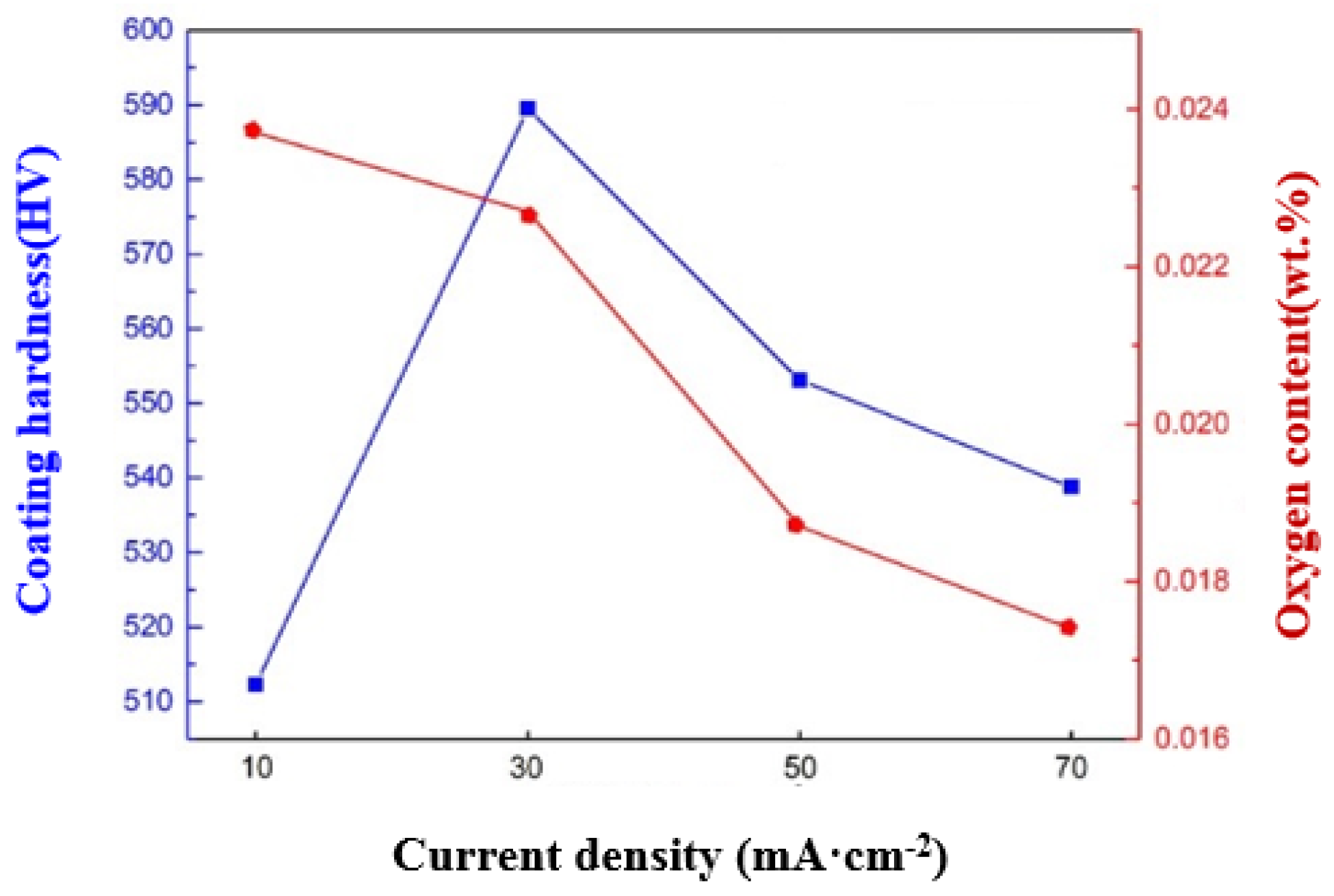
3.2. Performance Evaluation of Thick Tungsten Coatings

In this experiment, the tensile method was employed to assess the adhesive strength between the thick coating and the substrate. The bonding strengths are presented in Table 1. The bonding strength between the tungsten coating and the steel matrix, prepared via molten salt electrodeposition, exceeds 45 MPa. Notably, the bonding strength achieved at a current density of 50 mA/cm2 reaches up to 51.22 MPa, which may be attributed to the denser microstructure of the coating [18].
To characterize the mechanical properties of tungsten coatings on 9Cr-ODS steel substrates prepared by pulsed electrodeposition in molten salt, microhardness tests were conducted on polished samples. Figure 10 illustrates the trends in hardness and oxygen content of the tungsten coatings as a function of different pulse current densities. At a current density of 10 mA·cm−2, the hardness is measured at 512.52 HV. As the current density increases to 30 mA·cm−2, the hardness rises to 589.55 HV. Further increasing the current density to 50 mA·cm−2 results in a decrease in hardness to 553.11 HV. When the current density reaches its maximum value of 70 mA·cm−2, the hardness decreases to 538.75 HV.
The trend chart of hardness indicates that at low current densities, the substrate significantly influences the coating’s hardness. As current density increases, the coating thickness also increases, thereby reducing the substrate’s influence on hardness while increasing the effect of grain size. Generally, smaller metal grains result in more grain boundaries, which create greater obstacles to dislocation movement and increase resistance to deformation, leading to higher hardness and strength. Conversely, as grain size increases, the number of grain boundaries within the same region decreases, resulting in lower hardness values. Therefore, continued increases in current density lead to a decrease in hardness.
The oxygen content in the tungsten coatings on 9Cr-ODS steel substrate represents a critical performance parameter. At a current density of 10 mA·cm−2, the oxygen content is measured at 0.0237 wt%. When the current density is increased to 70 mA·cm−2, the oxygen content in the coating decreases slightly to 0.0174 wt%. The variation in current density has a minimal impact on the oxygen content, indicating that the tungsten coating prepared under these conditions exhibits consistently low oxygen levels.

4. Conclusions

In this paper, tungsten coatings were obtained from Na2WO4−WO3 molten salt on the surface of 9Cr-ODS steel substrate at 1173 K, 30% duty cycle, and 1000 Hz frequency, with current density changing from 10 mA/cm2 to 70 mA/cm2. The microstructure and crystal structure of tungsten coatings were studied. The hardness and oxygen content of thick tungsten coatings were measured. The main conclusions are as follows:
(1) Dense and uniform single-phase tungsten coatings were successfully prepared on 9Cr-ODS steel substrate via pulsed electrodeposition from a Na2WO4−WO3 molten salt system. The coating demonstrated superior adhesion to the steel substrate, with no observable signs of cracking or delamination, and the bonding strength exceeded 45 MPa.
(2) The microstructure of the tungsten coating is significantly influenced by variations in current density. As the current density increases, both the grain size and thickness of the tungsten coating exhibit a corresponding increase, reaching maximum values of 8.03 μm and 60.65 μm, respectively. Regardless of the specific current density, the tungsten coating consistently displays a columnar crystalline structure. As the current density increases, the hardness initially rises and then declines, while the oxygen content in the coating progressively decreases.

Author Contributions

Conceptualization, Y.Z.; methodology, Y.L. and X.D.; formal analysis, Y.L.; investigation, Y.L. and X.D.; resources, Y.Z.; data curation, Y.L., Z.G., Y.Y. and X.D.; writing—original draft preparation, X.D.; writing—review and editing, Y.L.; supervision, Y.L.; project administration, Y.Z.; funding acquisition, Y.Z. All authors have read and agreed to the published version of the manuscript.

Funding

This study was supported by the National MCF Energy R&D Program (No. 2019YFE03130002).

Institutional Review Board Statement

Not applicable.

Informed Consent Statement

Not applicable.

Data Availability Statement

The original contributions presented in this study are included in the article. Further inquiries can be directed to the corresponding author.

Conflicts of Interest

The authors declare no conflict of interest.

References

  1. Gonzalez-Arrabal, R.; Mendez-González, Y.; Perlado, J.M. Sputtering fabrication of isolated W nanocolumns: A possible al-ternative as plasma facing material for nuclear fusion reactors. Nucl. Mater. Energy 2024, 40, 101704. [Google Scholar] [CrossRef]
  2. Piip, K.; Paris, P.; Hakola, A.; Bystrov, K.; De Temmerman, G.; Aints, M.; Jõgi, I.; Kozlova, J.; Laan, M.; Likonen, J.; et al. Influence of He/d2 Plasma Fluxes on the Morphology and Crystallinity of Tungsten Coatings. Phys. Scr. 2014, 89, 044009. [Google Scholar] [CrossRef]
  3. Ribis, J.; Bordas, E.; Trocellier, P.; Serruys, Y.; de Carlan, Y.; Legris, A. Comparison of the neutron and ion irradiation response of nano-oxides in oxide dispersion strengthened materials. J. Mater. Res. 2015, 30, 2210–2221. [Google Scholar] [CrossRef]
  4. Xu, Y.; Tian, X.P.; Tan, H.Y.; Fu, H.Y.; Ni, J.J.; Luo, L.M.; Wu, Y.C. Effects of helium irradiation damage on deuterium plasma-driven permeation through tungsten coated RAFM steel. Nucl. Fusion 2025, 65, 026056. [Google Scholar] [CrossRef]
  5. Lee, J.; Shin, Y.C. Crack-free tungsten coating on ods plate via a modified laser-based additive technique: Offset laser cladding. Surf. Coat. Technol. 2024, 476, 130285. [Google Scholar] [CrossRef]
  6. Matthews, G.F.; Coad, P.; Greuner, H.; Hill, M.; Hirai, T.; Likonen, J.; Maier, H.; Mayer, M.; Neu, R.; Philipps, V.; et al. Development of divertor tungsten coatings for the JET ITER-like wall. J. Nucl. Mater. 2009, 390–391, 934–937. [Google Scholar] [CrossRef]
  7. Wan, B.; Ding, S.; Qian, J.; Li, G.; Xiao, B.; Xu, G. Physics Design of CFETR: Determination of the Device Engineering Parameters. IEEE Trans. Plasma Sci. 2014, 42, 495–502. [Google Scholar] [CrossRef]
  8. Matějíček, J.; Vilémová, M.; Mušálek, R.; Sachr, P.; Horník, J. The Influence of Interface Characteristics on the Adhesion/Cohesion of Plasma Sprayed Tungsten Coatings. Coatings 2013, 3, 108–125. [Google Scholar] [CrossRef]
  9. Strekalina, D.; Dushik, V.; Shaporenkov, A.; Tatiana, L.; Bukatin, T. Prospects of tungsten CVD technology for electric vehicles. AIP Conf. Proc. 2024, 3154, 020018. [Google Scholar] [CrossRef]
  10. Han, X.Y.; Liu, X.L.; Wang, D.Z.; Wu, Z.; Duan, B. Copper-based tungsten coating by CVD: Microstructure, thermal shock resistance and interfacial bond force. Surf. Coat. Technol. 2021, 426, 127778. [Google Scholar] [CrossRef]
  11. Sun, N.B.; Zhang, Y.C.; Lang, S.T.; Jiang, F.; Wang, L.L. Tungsten coatings electro-deposited on CFC substrates from oxide molten salt. J. Nucl. Mater. 2014, 455, 450–453. [Google Scholar] [CrossRef]
  12. Tokunaga, K.; Yoshida, N.; Kubota, Y.; Noda, N.; Imamura, Y.; Oku, T.; Kurumada, A.; Sogabe, T.; Kato, T.; Plöchl, L. High heat flux test of actively cooled tungsten-coated carbon divertor mock-ups. Fusion Eng. Des. 2000, 49–50, 371–376. [Google Scholar] [CrossRef]
  13. Matějíček, J.; Koza, Y.; Weinzettl, V. Plasma sprayed tungsten-based coatings and their performance under fusion relevant conditions. Fusion Eng. Des. 2005, 75–79, 395–399. [Google Scholar] [CrossRef]
  14. Liu, Y.H.; Zhang, Y.C.; Liu, Q.Z.; Li, X.L.; Jiang, F. The effects of electro-deposition current parameters on performance of tungsten coating. Int. J. Refract. Met. Hard Mater. 2012, 35, 241–245. [Google Scholar] [CrossRef]
  15. Lian, Y.Y.; Liu, X.; Xu, Z.Y.; Song, J.P.; Yu, Y. Preparation and properties of CVD-W coated W/Cu FGM mock-ups. Fusion Eng. Des. 2013, 88, 1694–1698. [Google Scholar] [CrossRef]
  16. Horník, J.; Tondl, D.; Sachr, P.; Anisimov, E.; Puchnin, M.; Chraska, T. The Effect of PVD Tungsten-Based Coatings on Improvement of Hardness and Wear Resistance. Key Eng. Mater. 2014, 606, 163–166. [Google Scholar] [CrossRef]
  17. Deng, C.; Liu, M.; Yang, Z.; Deng, C.; Zhou, K.; Kuang, Z.; Zhang, J. Manufacture of thick VPS W coatings on relatively large CuZrCr substrate and its steady high heat load performance. J. Nucl. Mater. 2014, 455, 145–150. [Google Scholar] [CrossRef]
  18. Zhang, Z.C.; Liu, Z.Q.; Cai, Y.K.; Wang, B.; Song, Q.H. Effect of Coating Thickness on the Bond Strength of Cold-Sprayed Ni-Based cBN Coating on 42CrMo Substrate. J. Therm. Spray Technol. 2023, 32, 1554–1569. [Google Scholar] [CrossRef]
Figure 1. Macroscopic morphology of tungsten coatings prepared at different current densities: (a) 10 mA·cm−2; (b) 30 mA·cm−2; (c) 50 mA·cm−2; (d) 70 mA·cm−2.
Coatings 15 00257 g001
Figure 2. Surface SEM images of the tungsten coatings prepared at different current densities: (a) 10 mA·cm−2; (b) 30 mA·cm−2; (c) 50 mA·cm−2; (d) 70 mA·cm−2.
Coatings 15 00257 g002
Figure 3. Effect of different pulse current densities on grain size of tungsten coatings.
Coatings 15 00257 g003
Figure 4. XRD patterns of tungsten coatings prepared at different current densities: (a) 10 mA·cm−2; (b) 30 mA·cm−2; (c) 50 mA·cm−2; (d) 70 mA·cm−2.
Coatings 15 00257 g004
Figure 5. XPS spectrum of tungsten coating prepared at 50 mA·cm−2 current density.
Coatings 15 00257 g005
Figure 6. Cross-sectional SEM images of tungsten coatings prepared at different current densities: (a) 10 mA·cm−2; (b) 30 mA·cm−2; (c) 50 mA·cm−2; (d) 70 mA·cm−2.
Coatings 15 00257 g006
Figure 7. Fracture SEM images of coatings prepared at different current densities: (a) 10 mA·cm−2; (b) 30 mA·cm−2; (c) 50 mA·cm−2; (d) 70 mA·cm−2.
Coatings 15 00257 g007
Figure 8. Schematic diagram of pulse electrodeposition waveform.
Coatings 15 00257 g008
Figure 9. Schematic representation of the electrochemical process for the electrodeposition of a tungsten coating on the substrate surface during a single pulse period.
Coatings 15 00257 g009
Figure 10. Effect of different pulse current densities on hardness and oxygen content of tungsten coatings.
Coatings 15 00257 g010
Table 1. Bonding strength of tungsten coatings prepared by different current densities.
Current DensityBonding Strength (MPa)
10 mA/cm245.87
30 mA/cm247.56
50 mA/cm251.22
70 mA/cm249.33
Disclaimer/Publisher’s Note: The statements, opinions and data contained in all publications are solely those of the individual author(s) and contributor(s) and not of MDPI and/or the editor(s). MDPI and/or the editor(s) disclaim responsibility for any injury to people or property resulting from any ideas, methods, instructions or products referred to in the content.

