Abstract
Thin films of copper oxide (CuxO), titanium oxide (TiOx), and several mixtures of copper and titanium oxides ((CuTi)Ox) were deposited using magnetron sputtering. X-ray diffraction analysis of the as-deposited TiOx thin film revealed the presence of TiO crystallites, while in the case of (CuTi)Ox with the lowest amount of copper, metallic Cu crystallites were found. In the case of (Cu0.77Ti0.23)Ox and CuxO thin films, characteristic peaks for metallic copper and copper oxides were observed in their diffractograms. It was found that post-process annealing at 473 K considerably affects the microstructure of (CuTi)Ox thin films. After annealing, anatase phase was observed in (Cu0.23Ti0.77)Ox and (Cu0.41Ti0.59)Ox thin films. In turn, the (Cu0.77Ti0.23)Ox and CuxO films were formed only in the copper oxide phase. The (Cu0.77Ti0.23)Ox film annealed at 473 K showed the best opto-electronic performance, as it had the highest transmission and the lowest resistivity. However, the greatest advantage of this thin film was the p-type semiconducting behavior, which was the strongest of all of the thin films in this work, as indicated by the measurement of the Seebeck coefficient. All deposited thin films were sensitive to hydrogen exposure, while the best sensor response of 10.9 was observed for the (Cu0.77Ti0.23) Ox thin film annealed at 473 K.
1. Introduction
Over the decades, there has been a steadily growing interest in metal oxides as materials for gas sensors, transparent electronics, lithium-ion batteries, solar cells, and self-cleaning or electrochromic coatings [1,2,3,4,5,6]. The reasons for such a high interest include the relatively low cost of metal oxides, the ability to create an extensive surface area with respect to the volume of the material, and the catalytic efficiency. In addition, the deposition technologies of such oxides in the form of thin films are compatible with production technology such as MOS [7], which makes it possible to easily integrate various oxide-based active devices, such as sensors, with electronics circuits in a single device. Copper and titanium oxides are nontoxic compounds commonly found in the Earth’s crust. They exhibit many interesting optical, electrical, and chemical properties that can be customized due to their different application areas, e.g., high optical transmittance, semiconducting properties, and photocatalytic properties [8,9].
There are two stable forms of copper oxide: cuprous oxide (Cu2O) and cupric oxide (CuO) [10]. The former has a cubic crystal structure and the latter crystallizes in the monoclinic phase. The band gap of copper oxides (CuxO)—depending on the oxide form—is in the range of 1.2–2.1 eV and 2.1–2.6 eV for CuO and Cu2O, respectively [10]. Such narrow band gaps make them promising materials for solar energy conversion [11]. Moreover, CuxO can be an interesting material for gas sensing applications [8,12] or for transparent electronic devices [3,13] since both copper oxides are well-known p-type oxide semiconductors. Their hole-type conduction is due to the presence of negatively charged Cu vacancies. The great advantage of Cu2O is one of the highest reported hole mobility (exceeding 100 cm2/Vs), which is caused by its unique band structure. Unlike other metal oxides, the valence band of the cupric oxide is formed of hybridized Cu 3d and O 2p orbitals that leads to the creation of a less localized hole transport pathway [14,15,16].
One of the simplest methods to obtain CuxO thin films is thermal oxidation of metallic copper foil. Annealing at 473 K initiates partial oxidation of Cu2O, a further increase in temperature to 573 K results in the formation of a mixed phase of Cu2O and CuO, and finally above 623 K, a single cupric oxide is formed [8].
On the other hand, titanium dioxide (TiO2) is a well-known photocatalyst [4,17]. It may crystallize in two stable tetragonal forms, anatase and rutile. A moderately wide band gap of 3.0–3.4 eV contributes to excellent transparency in the visible wavelength range. However, in the case of optoelectronic applications, an improvement of electrical parameters is necessary [3] as stoichiometric titanium dioxide at room temperature is an insulator [18]. The deposition of non-stoichiometric oxide with oxygen vacancies that cause intrinsic n-type semiconducting behavior could be one of the methods for modification of electronic properties. Therefore, the combination of good optical properties of titanium oxide with p-type conduction of copper oxides could result in formation of an attractive material for optoelectronic application.
For the production of technologically advanced transparent electronic devices or for the practical realization of such a sensor device as an electronic nose, it is necessary to combine p-type and n-type oxides. Recently, n-type metal oxides such as SnO2 or In2O3 have been successfully applied in commercial electronic devices, but their p-type counterparts still lack performance. Therefore, the development of p-type semiconducting metal oxides is still a strategic issue. The (CuTi)Ox thin films appear to be one of the most attractive systems. For example, Mor et al. [15] successfully manufactured the (CuTi)Ox(p)–TiO2(n) junction and showed that (CuTi)Ox, depending on the copper concentration, it can possess n-type properties for the lowest copper concentration [15] and p-type properties when the amount of copper increases [3,19]. Likewise, the optical properties of mixed copper and titanium oxide depend on the concentration of copper oxides [20]. However, it is possible to produce transparent [3] or semitransparent [13,20] semiconducting (CuTi)Ox thin films called transparent oxide semiconductors (TOS). Furthermore, the aforementioned p-type composite system exhibits gas sensing properties to NO2, O3, Cl2, H2, CH3COH, and Cl2 at moderate working temperatures [21,22,23] and the interactions between the sensor surface and the gas can be advantageously altered by doping with Li [22] or Au [23]. Barreca et al. [23] reported that the addition of titanium oxide can improve the performance of copper oxide as an electrode for lithium-ion batteries. Incorporation of CuxO into the TiO2 matrix improved photocatalytic activity in the case of pollution decomposition [24,25,26,27] including CO2 reduction [28] and hydrogen generation in the photoinduced water splitting process [15,29,30,31,32]. Antimicrobacterial studies show that copper addition to TiO2 has a positive effect in reducing bacterial (e.g., E. coli) viability [2,33]. In turn, the fabrication of coatings with gradient elemental distribution resulted in the formation of copper-reach regions of (CuTi)Ox, which acted as a semiconducting material, and copper-poor regions, which acted as an insulating material. This structure exhibited memristive properties without the necessity of depositing multilayer structures [19,34,35].
Mixed copper and titanium oxides have recently been prepared by microwave-assisted synthesis [24], ion beam sputtering [21,36], anodization of Cu-Ti films deposited by magnetron sputtering [15], low pressure CVD [23,37], or sol–gel [30,38]. In our previous works [3,19,34,35], preparation of (CuTi)Ox thin films using magnetron sputtering has also been described. In this paper, we propose a two-step preparation route: (1) deposition of not fully oxidized thin films using magnetron sputtering method and (2) additional post-process annealing at 473 K for tailoring of the thin film properties. To our knowledge, the composite material of mixed copper and titanium oxides with such a variety of copper concentrations (23–77 at.%) has never been thoroughly analyzed. The aim of the work was to obtain material with good optoelectronic properties, which is not an obvious task, since enhancing the electrical properties usually results in deterioration of the material’s transparency. The idea was to obtain a composite material in which one component possesses excellent transparency and the other is a desirable p-type oxide semiconductor, in order to enhance the dominance of the hole conduction type in the material, lowering its resistivity, while obtaining moderate transparency. Furthermore, results of investigations of the prepared sensor response to hydrogen have been demonstrated at a low operating temperature of 473 K.
2. Materials and Methods
The copper and titanium (CuTi)Ox mixed oxides thin films were deposited by the magnetron co-sputtering method using two circular titanium targets (99.999%) and one copper target (99.999%), each with a diameter of 28.5 mm and a thickness of 3 mm. A constant flow of argon and oxygen was provided during the deposition process, acting as the working and reactive gases, respectively. The amount of oxygen in the Ar − O2 gas mixture was equal to 15%. The base pressure was on the order of 10−5 mbar, while the pressure in the vacuum chamber during the sputtering was kept at approximately 1.25 × 10⁻² mbar. The magnetrons were powered using an MSS2 2 kW pulsed DC power supply unit (DORA Power System, Wilczyce, Poland). The power applied to each magnetron was a decisive factor in obtaining thin films with various material compositions, i.e., the copper–titanium ratio. The most crucial deposition parameters are summarized in Table 1.

Table 1.
Summary of the main process parameters for magnetron co-sputtering deposition of copper oxide (CuxO), titanium oxide (TiOx), and mixed copper and titanium oxides (CuTi)Ox.
No additional heating or electrical biasing of the substrate was used during the deposition. However, after the deposition process, (CuTi)Ox samples were additionally annealed in an air ambient at 473 K for 4 h. Thin films deposited on fused silica (SiO2) were used for structural and optical investigations, while scanning electron microscopy and energy-dispersive X-ray spectroscopy were performed for thin films deposited on n-type silicon substrates. For electrical measurements, ceramic substrates with interdigitated platinum-gold electrodes were used. The thickness of the thin films was measured using the Taylor Hobson optical profilometer (Talysurf CCI Lite, Leicester, UK) and was in the range of 430 to 620 nm.
The structure of the thin films was investigated by X-ray diffraction in the grazing incidence mode (GIXRD) using an Empyrean X-ray diffractometer (PANalytical, Malvern, UK) with a PIXel3D detector. The diffraction pattern was collected in the 2θ range of 20 to 80° using Cu Kα radiation (λ = 1.5406 Å). By comparing the obtained pattern with PDF cards (Cu #04-0836 [39], Cu2O #65-3288 [40], CuO #65-2309 [41], TiO #65-2900 [42], anatase #21-1272 [43]) a phase structure was determined. With the aid of MDI JADE 5.0 software, the average crystallite size was calculated using Scherrer’s equation [44].
The morphology and elemental composition were investigated using the SEM/Ga-FIB FEI Helios NanoLab 600i scanning electron microscope (FEI, Hillsboro, OR, USA) equipped with the energy dispersive X-ray spectrometer (EDS). Surface SEM imaging was expanded to cross-sectional profile studies.
The optical measurement workstation consisted of Ocean Optics QE 65000 and NIR 256-2.1 spectrophotometers (Ocean Optics, Largo, FL, USA) and a coupled deuterium–halogen light source. The transmission coefficient was determined from transmittance spectra measured in the wavelength range of 250 ÷ 2000 nm. The average transmission was evaluated by calculating the integral in visible wavelength range of 380 to 760 nm and in near infrared wavelength range of 760 to 2000 nm, while the position of the fundamental absorption edge was designated by fitting the descending to zero linear part of the transmission characteristic.
For electrical characterization, a M100 Cascade Microtech probe station (Cascade Microtech, Beaverton, OR, USA) and a Keithley SCS4200 system were used. Current–voltage characteristics were measured in a shielded Faraday cage at room temperature. Measurements were performed for temperature changing from 303 K to 353 K that allowed us to determine the activation energy. Thermoelectric characteristics were obtained using the FLUKE 8846A voltmeter (Fluke, Everett, WA, USA) and the Instek mK1000 temperature controller (GW Instek, Taipei, Taiwan). For the determination of the Seebeck coefficient [45] a temperature gradient (ΔT) between ‘hot’ and ‘cold’ electrical contacts was applied in the range from 0 to 50 K, as the ‘cold’ contact was kept at room temperature. The Seebeck coefficient (Sc) was calculated according to Equation (1) and the conduction type was evaluated based on the sign of the obtained values:
where Sc is the Seebeck coefficient, ΔU is the difference in thermoelectric voltage, and ΔT is the temperature gradient.
Furthermore, the gas sensing properties of annealed (CuTi)Ox thin films were investigated for 3.5% of H2 diluted in Ar. Measurements were performed in a self-assembled system equipped with an Agilent 34,901A data acquisition system; Instec mK1000 temperature controller; and a mass flow controller. Before injection of H2, the thin films were heated on a heating table to an operating temperature equal to 473 K and stabilized in an air environment for an hour.
3. Results
3.1. Microstructure and Morphology
Figure 1 presents results of X-ray microanalysis investigations for as-deposited thin oxide films of copper (CuxO), titanium (TiOx) and of four oxide mixtures with various concentrations of copper and titanium ((CuTi)Ox). As one can see, in the energy range of 4 to 10 keV only TiKα, TiKβ peaks were recognized in the spectrum attributed to the TiOx thin film and only CuKα and CuKβ peaks were found in the CuxO spectrum. Furthermore, as the copper concentration increased, the ratio of CuKα to TiKα increased simultaneously. The atomic content of copper in the thin films of oxide mixtures was estimated to be 23 at.%, 41 at.%, 56 at.%, and 77 at.%. The distribution maps of Cu, Ti, and O presented in Figure 1b show a homogeneous dispersion of each element in the thin films. A decisive factor in obtaining various elemental compositions in the deposited thin films was a proper regulation of the sputtering power supplying of each magnetron. Figure 2 presents the copper concentration in the thin film as a function of the ratio of the sputtering power at the Cu target (PCu) to the total power at the three targets (PCu + PTi). As expected, the increase in the PCu/(PCu + PTi) ratio resulted in a higher amount of copper in the thin film.
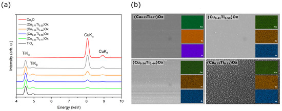
Figure 1.
Results of X-ray microanalysis investigations for as-deposited copper and titanium oxide thin films: (a) EDS spectra and (b) maps of elemental distribution of mixed oxides.
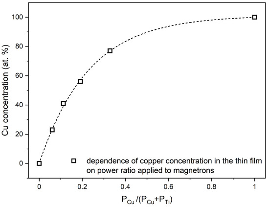
Figure 2.
Dependence of copper content in as-deposited thin films on the power ratio PCu/(PCu + PTi) applied to magnetrons with Cu and Ti targets.
The morphology of the deposited thin films was investigated using scanning electron microscopy. The elemental composition strongly affects the morphology of the thin films, as can be deduced from the SEM images presented in Figure 3. The surface of the as-deposited TiOx thin film was relatively smooth with some visible voids. The cross-sectional image revealed that it was composed of densely packed columnar grains. In contrast, the morphology of oxide mixtures with the 23, 41, and 56 at.% of copper differs significantly from TiOx, as the columnar character changed to elongated and coarse grains. The surfaces were relatively flat and crack-free. Furthermore, single nanowires were formed at the top of (Cu0.23Ti0.77)Ox. It is worth mentioning that when the copper content increased to 77 at.%, the morphology of oxides changed considerably. The grains were bulb-shaped, smaller at the bottom, and widen upward. Each bulb-shaped grain had a granular surface that resembles cauliflower. Such a grain shape resulted in the largest active surface of all of the as-deposited thin films, which is highly desirable in the case of photocatalytic activity or gas-sensing properties [23]. Compared to other thin films, (Cu0.77Ti0.23)Ox had the largest grains of ca. 250–300 nm and intergrain spaces (voids). The surface of copper oxide thin film was more homogeneous, the grains were still clearly visible, but the voids between them were smaller. Furthermore, the shape of the grains was also different—that is, they were elongated, granular, and more densely packed as compared to the oxide mixture with 77 at.% Cu.
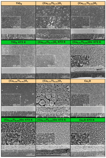
Figure 3.
Scanning electron microscopy images of the surface and cross-section of as-deposited and annealed at 473 K TiOx, (CuTi)Ox, and CuxO thin films.
After annealing at 473 K, no significant changes occurred on the surface of the TiOx thin film, but thermal oxidation considerably influenced the morphology of the oxide mixtures. It can be clearly seen from the cross-sectional images of the annealed thin films containing 23, 41, and 56 at.%, that at the bottom the elongated grains grow perpendicularly to the substrate surface, while close to the surface, they became grainy and rough. In addition, the grainy, sponge-shaped structure was thicker as the amount of copper in the thin film increased. The thin films were made up of grains smaller than 100 nm. The (Cu0.77Ti0.23)Ox was spongy in nature throughout its thickness. There were apparent interlayer voids of various shapes and sizes. For annealed CuxO thin films, the structure remains porous. However, the vertical orientation of the grains was favorable. Furthermore, the voids were smaller and uniformly distributed.
XRD analysis was performed to determine the structural properties of the prepared thin films (Figure 4a). In the diffraction pattern of the TiOx thin film, three characteristic peaks attributed to the (111), (200), and (220) planes of the TiO phase were observed, while no characteristic peaks of TiO2 anatase or rutile were found. The size of the crystallites of the TiO phase was in the range from 4.9 to 11.8 nm, as calculated according to Scherrer’s formula (Equation (2)):
where k = 0.89 is the shape factor, λ is the CuKα X-ray radiation wavelength (1.5406 Å), B is the full width at half maximum intensity of the peak (FWHM), and θ is a diffraction angle.
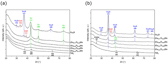
Figure 4.
X-ray diffraction patterns of (a) as-deposited and (b) annealed at 473 K (CuTi)Ox thin films.
In each diffractogram of the copper and titanium oxide mixtures, a peak occurring at 2θ = 42.7° is associated with the metallic copper (111) lattice plane. As the amount of copper in the thin film increased, the character of this peak changed significantly from very wide and poorly defined to sharp and intense. The crystallite size of the Cu (111) phase varied from ca. 3.0 to 13.4 nm. For (Cu0.77Ti0.23)Ox thin film, in addition to the most dominant Cu (111) peak, reflections from Cu (200), (220), Cu2O (111), and CuO (111) were detected. The Cu2O-cubic phase was characterized by the smallest crystallite size, which was equal to 5.1 nm, since the peak was broad, while metallic copper crystallites were equal to 13.4 nm. The copper oxide thin film consisted of the same metallic Cu peaks, but they are less intense, and the crystallite size was considerably smaller. In addition to the most intense peak of Cu2O (111), there are also weaker reflections of Cu2O (110) and Cu2O (220) observed at 2θ = 29.88° and 61.86°, respectively. Furthermore, a peak centered at 33.1° was attributed to the crystalline phase of CuO (110). However, as the titanium concentration in the thin films of oxide mixtures was decreasing, the copper was more oxidized.
Post-process annealing at 473 K did not significantly affect the TiOx thin film microstructure. The sample was still mostly amorphous in nature, but a TiO crystalline phase was observed. The most intense peak was attributed to the (200) crystal plane. Moreover, the crystallite size remained similar (ca. 5 nm) to that before annealing. Thermal oxidation of the thin films of oxide mixtures with a Ti content greater than 50% resulted in crystallization of the anatase. A strong peak of the anatase crystal plane (101) was found at 2θ = 25.2°, but when the amount of copper exceeded that of titanium, no anatase phase was observed. Similarly to the as-deposited thin films, the metallic copper reflections from the (111) plane was found in the diffractogram of the annealed thin films containing 23 at.%, 41 at.%, and 56 at.% of Cu; however, the intensity of the peaks decreased. Furthermore, characteristic Cu2O peaks were found in addition to metallic copper, suggesting that annealing at 473 K causes oxidation of the metallic Cu to Cu2O. It should be emphasised that in the (Cu0.77Ti0.23)Ox thin film, the phase transition was completed, as no Cu peaks were observed. The (111) crystal plane was the most preferable orientation for Cu2O and was observed at 2θ = 29.63° and its intensity increased with increasing amount of copper in the thin film. The diffraction pattern of the thin films with the highest copper concentration additionally consisted of Cu2O peaks corresponding to the (110), (200), (220), (311), and (222) planes. All cuprous oxide crystallites were smaller than 13 nm. Moreover, a minor phase of CuO was also detected. The results of the X-ray investigations are summarized in Table 2.
Table 2.
Summary x-ray diffraction structure analysis of as-deposited and annealed (CuTi)Ox thin films.
Both copper and titanium strongly affect the crystal structure and the oxidation state in the oxide mixtures, as in as-deposited and annealed thin films. With decreasing amount of titanium, the phase transformation process from Cu to Cu2O and finally to CuO is more advanced. This can be explained by the fact that Ti exhibits high affinity to oxygen and, consequently, a high Ti concentration limits the oxidation of copper [46,47,48]. In turn, after post-process treatment, the peaks from the anatase phase were observed only in the oxide mixtures with the lowest copper concentration (23 at.% and 41 at.%), confirming that the high concentration of copper hinders the crystallization of anatase or rutile [13,20,33,49].
3.2. Electrical and Optical Properties
The type of electrical conduction was determined by observation of the sign of the Seebeck coefficient (Sc) calculated from the thermoelectrical power measurements (Figure 5). A positive sign of the Sc indicates the hole type of conduction, while the negative value testifies about electron type of electrical conduction. The TiOx thin film exhibited the strongest n-type properties of all as-deposited thin films and the Seebeck coefficient was equal to −25 μV/K. The Sc value gradually increased as the amount of copper in the thin film increased and the change in the type of conduction was observed when the copper concentration exceeded 56 at.%. The thin films with the highest copper content were characterized by weak p-type conduction. For the CuxO thin film, the Seebeck coefficient was equal to +6.1 μV/K. Post-process annealing significantly influenced the conduction type of thin films consisting of crystalline copper and copper oxides, as samples were characterized by a hole type of electrical conduction (Figure 5c). Furthermore, it should be noted that the studies of copper and titanium oxide mixtures annealed at 473 K have shown that the Seebeck coefficient of the (Cu0.56Ti0.44)Ox and (Cu0.77Ti0.23)Ox thin films was significantly higher compared to CuxO thin film for which the Sc coefficient was +245.1 μV/K. Copper oxides are well-known semiconductors with strong p-type properties [10], while TiO2 is reported to be an n-type semiconductor [18]. When it comes to mixed copper-titanium oxides phase, Mor [15] et al. showed for Cu-Ti-O nanotubes fabricated by anodization of Cu-Ti films that the conduction type depends on the copper concentration. The sample with a Cu:Ti ratio equal to 24:76 was characterized by n-type conduction, while for ratios of 60:40 and 74:26, the samples were p-type semiconductors.
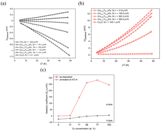
Figure 5.
Thermoelectric characteristics of: (a) as-deposited, (b) annealed at 473 K (CuTi)Ox thin films, and (c) Seebeck coefficient changes depending on the elemental composition and annealing of the thin films.
Investigations of electrical properties were extended with measurements of the current–voltage characteristics, performed at room temperature and at elevated temperature (from 303 to 353 K). For all samples, the characteristics were linear and high repeatability was observed. Based on the Arrhenius formula (Equation (3)) and the slope of the fit of log (ρ) = f(1000/T) plot, the activation energy was calculated from
where k is the Boltzmann constant and T is the temperature.
The obtained electrical parameters are presented in Table 3. With the increase in the copper concentration in the thin film, the resistivity of the (CuTi)Ox gradually decreased and for thin films with 56 and 77 at.% of Cu was equal to 2.5·10−2 and 3.0·10−3 Ω cm, respectively (Figure 6). Annealing at 473 K caused an increase in the resistivity by ca. three orders of magnitude for all thin films except (Cu0.77Ti0.23)Ox for which the resistivity increased almost four orders of magnitude. The resistivity of the TiOx sample after thermal treatment was 3.8 × 10³ Ω cm. Titanium monoxide is generally perceived as an excellent conductor with a resistivity value in the range of 10−4–10−3 Ω cm [50,51,52,53]. However, there are also reports showing that the resistivity value of nanocrystalline TiO can be as high as 105 Ω cm [54]. Therefore, the resistivity value obtained in this work falls within the wide range reported in the literature, while its quite high value may be explained by a large amount of the amorphous phase present in the thin film, as evidenced by the low intensity of the peaks visible in the XRD (Figure 4). The CuxO and (Cu0.23Ti0.77)Ox thin films after annealing had a resistivity equal to ca. 7 × 10² Ω cm. The addition of 41 at.% of Cu caused a decrease in ρ by an order of magnitude compared to the TiOx sample. A further increase in the Cu content resulted in a gradual decrease in resistivity, which was equal to 41.5 Ω cm and 28.1 Ω cm for (Cu0.56Ti0.44)Ox and (Cu0.77Ti0.23)Ox.
Table 3.
Electrical parameters of as-deposited and annealed at 473 K (CuTi)Ox thin films.
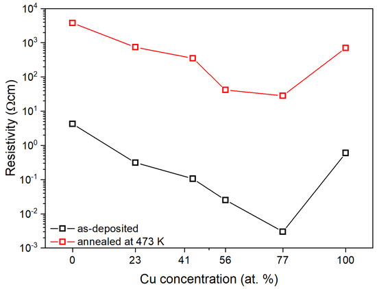
Figure 6.
Resistivity changes depending on elemental composition and annealing temperature.
Figure 7 presents the dependence of the resistivity vs. the temperature in the range from 303 K to 353 K. For the thin films with the lowest copper concentration, the resistivity gradually decreased with increasing temperature, while remaining constant when the Cu concentration in the film exceeded 50%. Almost no change in resistivity as a function of temperature indicated the very low activation energy of electrical conduction processes that might be connected with the presence of metallic Cu species in those thin films.
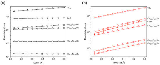
Figure 7.
Temperature dependent resistivity of (a) as-deposited and (b) annealed at 473 K thin films.
In each case of annealed thin films, the resistivity was found to decrease with increasing temperature. The activation energy was in the range from 0.26 to 0.35 eV/K indicating the semiconducting nature of the (CuTi)Ox thin films after thermal oxidation.
The optical properties of the (CuTi)Ox thin films were determined on the basis of the transmission measurements of light in the wavelength range from 250 nm to 2000 nm. All as-deposited thin films were opaque, which could be the consequence of the low oxygen concentration during the sputtering process [55], resulting in the presence of metallic copper crystallites in the CuxO and in (CuTi)Ox thin films. In the visible wavelength range, the transmission of the as-deposited thin films was less than 2%. As can be seen in Figure 8, the post-process thermal treatment strongly influenced the optical properties of the TiOx, (Cu0.77Ti0.23)Ox and CuxO thin films as they oxidized and became transparent, mainly in the infrared region. Moreover, interference fringes began to appear. However, the samples with 23, 41, and 56 at.% of Cu remained opaque. The absorption edge of the TiOx thin film was positioned at the cut-off wavelength (λcut-off) equal to 339 nm, while a redshift to ca. 490 nm was observed for the (Cu0.77Ti0.23)Ox and pure copper oxide films. This observation is consistent with the data reported for λcut-off for non-stoichiometric TiOx and CuxO thin films [56,57]. The average transmittance of TiOx in the visible wavelength range was equal to 11%, while for the (Cu0.77Ti0.23)Ox and CuxO thin films it was equal to 22% and 27%, respectively. In turn, in the near infrared wavelength range the average transmittance increased slightly for the TiOx and was equal to 21%, but for the (Cu0.77Ti0.23)Ox and CuxO thin films it was even ca. 70%.
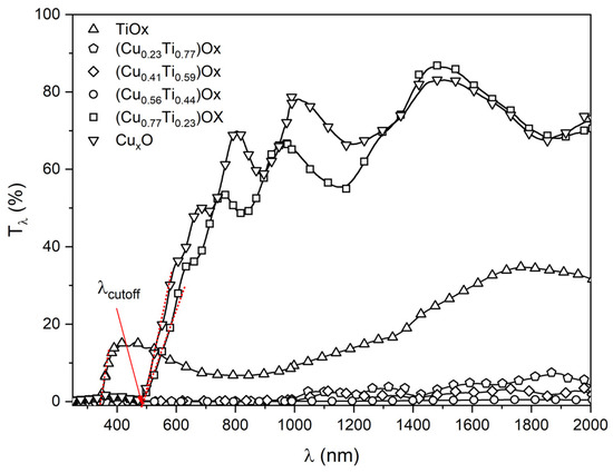
Figure 8.
Transmission characteristic of thin films annealed at 473 K.
3.3. Hydrogen Gas Sensing
Figure 9 presents the dynamic sensor response of the annealed titanium oxide, oxide mixtures, and copper oxide thin films exposed to 3.5% hydrogen diluted in argon at an operating temperature of 473 K. Titanium oxide showed the electron conduction type as its resistance decreased in the presence of the reducing gas (H2). The opposite effect was observed for the (CuTi)Ox and CuxO, indicating that holes were the dominant electrical charge carriers. Therefore, the conduction type designated on the basis of the gas sensing characteristics was consistent with the thermoelectric measurements. The sensing mechanism in metal oxide semiconductors is a complex issue as it depends not only on the material composition and conduction type, but also on their morphology, grain size, gas concentration, operating temperature, and humidity condition [58]. In general, in the case of metal oxide structures, the dominant role is in adsorption and desorption processes on the surface of the thin film. In air, oxygen molecules are adsorbed at the surface of sensing material in the form of O2−, O−, or O2− depending on working temperature. Temperatures above 423 K dominate the adsorption of O− or O2− species [59]. The oxygen adsorption might follow as in Equations (4) and (5):
O2 (gas) + e− ↔ O2−
O2 (gas) + 2e− ↔ 2O−
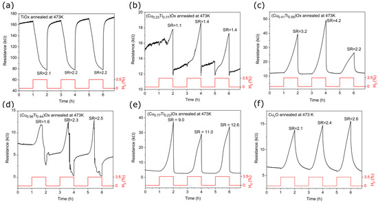
Figure 9.
Resistance changes of: (a) TiOx, (b–e) (CuTi)Ox, and (f) CuxO thin films annealed at 473 K upon exposure to 3.5% H2.
Chemisorbed oxygen extracts electrons from the surface, forming an electron depletion layer. For n-type semiconductors, the resistance of the depleted layer is higher than that of the bulk material, causing the current to follow through the bulk grain. However, for p-type materials, the opposite phenomenon is observed: the hole accumulation area is less resistive [6]. The introduction of hydrogen (a reducing gas) causes a reaction with chemisorbed oxygen according to the equation [60]
H2 (gas) + O− ↔ H2O(gas) + e−
As a result of the interaction of hydrogen with metal oxide, electrons are donated back to the conduction band, which occurs as an increase in the resistance for p-type materials and a decrease in the resistance for n-type materials.
The sensor response (SR) was calculated as the ratio of the resistance of the thin film in the air (Rair) to the resistance in the presence of hydrogen (RH2) for the TiOx thin film [61] and as the ratio of RH2 to Rair for the other thin films. Furthermore, the response and recovery times defined as the time required to reach 90% of the difference between Rair and RH2 were determined and summarised in Table 4.
Table 4.
Summary of sensing parameters of TiOx, CuxO, and (CuTi)Ox thin films annealed at 473 K.
The SR value for TiOx and CuxO was similar and equal to 2.2 and 2.4, respectively. As shown in Figure 9a, the titanium oxide response began to saturate after ca. 30 min of hydrogen flow and after ca. 5 min of air flow. The consequence of this was the short response and recovery time compared to those of CuxO, whose signal was far from saturation. Metal oxides that exhibit the p-type of electrical conduction typically respond worse than their n-type counterparts [6,62], however, the slightly better CuxO response may be caused by a considerable difference in the morphology and structure of the two thin films. As shown in the SEM images, titanium oxide annealed at 473 K had a dense and flat surface morphology, while copper oxide after the same thermal treatment was porous, resulting in a larger active surface area. In addition, the copper oxide crystallites were well-defined, whereas the titanium oxide thin film was mostly amorphous.
As can be concluded, the preparation of a composite of metal oxides can noticeably improve sensing capabilities—e.g., sensitivity and selectivity [58]—compared to a sensing material consisting of one of the components. In the case of heterostructures, the sensing response is determined by changes in the width of the charge depletion layer that is formed when the Fermi levels of the two metal oxides equilibrate and charge transfer occurs [63]. The undoubted advantage of oxide mixture thin films over double-layer structures is the better interaction of the reducing/oxidizing gas with p–n areas, since both the p-type and the n-type oxides are present at the surface simultaneously. This leads to a stronger manipulation of the p–n junction performance. It should be noted that in mixed composite structures not only the elemental composition of the thin film but also the dispersion state of the component are important [58].
In this work, a significant improvement in the gas detection response was observed for the (Cu0.77Ti0.23)Ox and (Cu0.41Ti0.59)Ox thin films compared to TiOx and CuxO. Sensor response of the thin film containing 77 at.% of Cu was more than 4.5 times higher than that of CuxO. The thin film with 23 at.% of Cu showed the worst H2 detection abilities, while in the case of (Cu0.56Ti0.44)Ox, the unique behavior was observed. As shown in Figure 9d under exposure to 3.5% H2, the resistance of the (Cu0.56Ti0.44)Ox thin film initially increased, but after a specific time decreased. Kosc et al. [64] reported a similar inversion of the response type in TiO2 modified with NiO structures in the presence of hydrogen. Inversion was observed when the hydrogen concentration exceeded a specific critical point. This unique behavior was explained by the fact that, when the amount of electrons from broken bonds of adsorbed oxygen exceeds the amount of holes in the Debaye length, the conduction type of heterostructure changes. In the ambient air atmosphere, the oxygen is re-adsorbed on the film surface causing the resistance to increase and reach the initial base value [58,64].
The resistance of the (CuTi)Ox thin films was constantly increasing throughout the hydrogen flow, and no signal plateau was observed, resulting in the response time exceeding 55 min. However, recovery times were relatively short. The best sensing performance to 3.5% H2 showed a thin film with 77 at.% of Cu as the sensor response was equal to 10.9 and the recovery time was the shortest of all measured thin films.
Comparing the sensing parameters of the (Cu0.77Ti0.23)Ox thin films to hydrogen with previously published works presented in Table 5, it can be seen that the sensor response is the highest among all the works reported so far. Similarly to this work, Park et al. [48] reported that the response time was shortened when TiO2 was added to the CuO nanorods. Furthermore, the recovery time increased after titanium dioxide modification and was in the range from 300 to 400 s. In turn, Alev et al. [63] reported that the response of TiO2 nanotubes covered with a CuO layer to 1000 ppm of H2 saturates in 15 min and the recovery time was equal to 10 min. The operating temperature applied in all the measurements of the response of copper and titanium oxide composites to hydrogen was in the range of 473 K to 673 K. Park et al. [48] and Alev [63] et al. presented findings that the optimal working temperature for their structures was 473 K, while for other structures higher temperatures were more desirable. In all articles summarized in Table 5, cupric oxide was the dominant phase of copper oxides. Our aim was to show that oxide mixtures of Cu2O and TiO2 can exhibit a good response to H2, while higher working temperature could cause oxidation to CuO, thereby hindering the SR value.
Table 5.
Gas sensing performance of copper oxide and titanium oxide composites toward hydrogen.
4. Summary
The purpose of this study was to investigate the selected properties of thin films of copper and titanium oxide mixtures. In this regard, the (CuTi)Ox thin films with various Cu concentrations were prepared using magnetron co-sputtering. In addition, post-process annealing at 473 K was applied to additionally oxidize deposited thin films. The as-deposited thin films had dense and well-packed structures. The copper concentration was equal to 23, 41, 56, and 77 at.%. XRD studies showed that the as-deposited oxide mixtures consisted of metallic copper and copper oxides crystallites. Post-process annealing resulted in a change in morphology to partially porous structures and caused crystallization of anatase and partial oxidation of copper to Cu2O or CuO. All annealed (CuTi)Ox thin films exhibited strong p-type semiconducting properties. Moreover, stronger hole-type conductivity was obtained in the (CuTi)Ox composite material than in the CuxO thin film. The (Cu0.77Ti0.23)Ox annealed at 473 K exhibited the best optoelectronic properties, as it was semitransparent in the visible radiation range, exhibited the strongest p-type conductivity and had the lowest resistivity of all deposited samples. Moreover, all the thin films responded to 3.5% hydrogen. These responses were characterized by long response times and very short recovery times. Again, the (Cu0.77Ti0.23)Ox sample exhibited the highest response (10.9 times).
As has been shown in this work, the hydrogen sensing properties of (CuTi)Ox thin films are promising, nevertheless, there is much to be done in the future works, e.g., further investigation of gas sensing properties to hydrogen of concentrations smaller than 1000 ppm and determination of chemical state of the surface are planned. The authors’ aim is to establish the mechanism responsible for the change in resistance under the influence of hydrogen. For that purpose, in-situ XPS measurements without and under the influence of hydrogen are scheduled to determine changes in oxidation states on the surface.
Author Contributions
Conceptualization, E.M. and M.M.; Methodology, E.M. and M.M.; Validation, E.M., M.M. and J.D.; Formal analysis, E.M.; Investigation, E.M., M.M., J.D. and D.W.; Resources, M.M.; Data curation, E.M.; Writing—original draft preparation, E.M., M.M. and J.D.; Writing—review and editing, E.M. and M.M.; Visualization, E.M.; Supervision, M.M.; Project administration, M.M.; Funding acquisition, M.M. All authors have read and agreed to the published version of the manuscript.
Funding
This work was co-financed from the sources given by the Polish National Science Center (NCN) as a research project number UMO-2018/29/B/ST8/00548 and UMO-2020/39/D/ST5/00424.
Institutional Review Board Statement
Not applicable.
Informed Consent Statement
Not applicable.
Data Availability Statement
Not applicable.
Acknowledgments
Authors would like to thank Danuta Kaczmarek for discussion on the investigation results.
Conflicts of Interest
The authors declare no conflict of interest.
References
- Wojcieszak, D.; Domaradzki, J.; Mazur, M.; Kotwica, T.; Kaczmarek, D. Investigation of a Memory Effect in a Au/(Ti–Cu)Ox-Gradient Thin Film/TiAlV Structure. Beilstein J. Nanotechnol. 2022, 13, 265–273. [Google Scholar] [CrossRef] [PubMed]
- Wojcieszak, D.; Mazur, M.; Kaczmarek, D.; Poniedziałek, A.; Osekowska, M. An Impact of the Copper Additive on Photocatalytic and Bactericidal Properties of TiO2 Thin Films. Mater. Sci. Pol. 2017, 35, 421–426. [Google Scholar] [CrossRef]
- Domaradzki, J. Perspectives of Development of TCO and TOS Thin Films Based on (Ti-Cu)Oxide Composites. Surf. Coatings Technol. 2016, 290, 28–33. [Google Scholar] [CrossRef]
- Nakata, K.; Fujishima, A. TiO2 Photocatalysis: Design and Applications. J. Photochem. Photobiol. C Photochem. Rev. 2012, 13, 169–189. [Google Scholar] [CrossRef]
- Livage, J.; Ganguli, D. Sol-Gel Electrochromic Coatings and Devices: A Review. Sol. Energy Mater. Sol. Cells 2001, 68, 365–381. [Google Scholar] [CrossRef]
- Maziarz, W. TiO2/SnO2 and TiO2/CuO Thin Film Nano-Heterostructures as Gas Sensors. Appl. Surf. Sci. 2019, 480, 361–370. [Google Scholar] [CrossRef]
- Nunes, D.; Pimentel, A.; Goncalves, A.; Pereira, S.; Branquinho, R.; Barquinha, P.; Fortunato, E.; Martins, R. Metal Oxide Nanostructures for Sensor Applications. Semicond. Sci. Technol. 2019, 34, 043001. [Google Scholar] [CrossRef]
- Wojcieszak, D.; Obstarczyk, A.; Mańkowska, E.; Mazur, M.; Kaczmarek, D.; Zakrzewska, K.; Mazur, P.; Domaradzki, J. Thermal Oxidation Impact on the Optoelectronic and Hydrogen Sensing Properties of P-Type Copper Oxide Thin Films. Mater. Res. Bull. 2022, 147, 111646. [Google Scholar] [CrossRef]
- Wiatrowski, A.; Wojcieszak, D.; Mazur, M.; Kaczmarek, D.; Domaradzki, J.; Kalisz, M.; Kijaszek, W.; Pokora, P.; Mańkowska, E.; Lubanska, A.; et al. Photocatalytic Coatings Based on TiOx for Application on Flexible Glass for Photovoltaic Panels. J. Mater. Eng. Perform. 2022, 31, 6998–7008. [Google Scholar] [CrossRef]
- Zoolfakar, A.S.; Rani, R.A.; Morfa, A.J.; O’Mullane, A.P.; Kalantar-Zadeh, K. Nanostructured Copper Oxide Semiconductors: A Perspective on Materials, Synthesis Methods and Applications. J. Mater. Chem. C 2014, 2, 5247–5270. [Google Scholar] [CrossRef]
- Dahl, M.; Liu, Y.; Yin, Y. Composite Titanium Dioxide Nanomaterials. Chem. Rev. 2014, 114, 9853–9889. [Google Scholar] [CrossRef]
- Rydosz, A. The Use of Copper Oxide Thin Films in Gas-Sensing Applications. Coatings 2018, 8, 425. [Google Scholar] [CrossRef]
- Barreca, D.; Battiston, G.A.; Casellato, U.; Gerbasi, R.; Tondello, E. Low Pressure CVD of Transparent Cu-Al-O and Cu-Ti-O Thin Films. J. Phys. IV 2001, 11, Pr11-253. [Google Scholar] [CrossRef]
- Wang, Z.; Nayak, P.K.; Caraveo-Frescas, J.A.; Alshareef, H.N. Recent Developments in P-Type Oxide Semiconductor Materials and Devices. Adv. Mater. 2016, 28, 3831–3892. [Google Scholar] [CrossRef]
- Mor, G.K.; Varghese, O.K.; Wilke, R.H.T.; Sharma, S.; Shankar, K.; Latempa, T.J.; Choi, K.S.; Grimes, C.A. P-Type Cu-Ti-O Nanotube Arrays and Their Use in Self-Biased Heterojunction Photoelectrochemical Diodes for Hydrogen Generation. Nano Lett. 2008, 8, 1906–1911. [Google Scholar] [CrossRef]
- Fortunato, E.; Figueiredo, V.; Barquinha, P.; Elamurugu, E.; Barros, R.; Goņalves, G.; Park, S.H.K.; Hwang, C.S.; Martins, R. Thin-Film Transistors Based on p-Type Cu2O Thin Films Produced at Room Temperature. Appl. Phys. Lett. 2010, 96, 2–5. [Google Scholar] [CrossRef]
- Mazur, M.; Wojcieszak, D.; Domaradzki, J.; Kaczmarek, D.; Song, S.; Placido, F. TiO2/SiO2 Multilayer as an Antireflective and Protective Coating Deposited by Microwave Assisted Magnetron Sputtering. Opto-Electron. Rev. 2013, 21, 233–238. [Google Scholar] [CrossRef]
- Nair, P.B.; Justinvictor, V.B.; Daniel, G.P.; Joy, K.; Ramakrishnan, V.; Thomas, P.V. Effect of RF Power and Sputtering Pressure on the Structural and Optical Properties of TiO2 Thin Films Prepared by RF Magnetron Sputtering. Appl. Surf. Sci. 2011, 257, 10869–10875. [Google Scholar] [CrossRef]
- Domaradzki, J.; Wiatrowski, A.; Kotwica, T.; Mazur, M. Analysis of Electrical Properties of Forward-to-Open (Ti,Cu)Ox Memristor Rectifier with Elemental Gradient Distribution Prepared Using (Multi)Magnetron Co-Sputtering Process. Mater. Sci. Semicond. Process. 2019, 94, 9–14. [Google Scholar] [CrossRef]
- Zhang, W.; Li, Y.; Zhu, S.; Wang, F. Copper Doping in Titanium Oxide Catalyst Film Prepared by Dc Reactive Magnetron Sputtering. Catal. Today 2004, 93–95, 589–594. [Google Scholar] [CrossRef]
- Torrisi, A.; Horák, P.; Vacík, J.; Cannavò, A.; Ceccio, G.; Yatskiv, R.; Kupcik, J.; Fara, J.; Fitl, P.; Vlcek, J.; et al. Preparation of Heterogenous Copper-Titanium Oxides for Chemiresistor Applications. Mater. Today Proc. 2019, 33, 2512–2516. [Google Scholar] [CrossRef]
- Torrisi, A.; Ceccio, G.; Cannav, A.; Lavrentiev, V.; Hor, P.; Yatskiv, R.; Vaniš, J.; Grym, J.; Fišer, L.; Hruška, M. Chemiresistors Based on Li-Doped CuO-TiO2 Films. Chemosensors 2021, 9, 246. [Google Scholar] [CrossRef]
- Barreca, D.; Carraro, G.; Comini, E.; Gasparotto, A.; MacCato, C.; Sada, C.; Sberveglieri, G.; Tondello, E. Novel Synthesis and Gas Sensing Performances of CuO-TiO2 Nanocomposites Functionalized with Au Nanoparticles. J. Phys. Chem. C 2011, 115, 10510–10517. [Google Scholar] [CrossRef]
- Kubiak, A.; Bielan, Z.; Kubacka, M.; Gabała, E.; Zgoła-Grześkowiak, A.; Janczarek, M.; Zalas, M.; Zielińska-Jurek, A.; Siwińska-Ciesielczyk, K.; Jesionowski, T. Microwave-Assisted Synthesis of a TiO2-CuO Heterojunction with Enhanced Photocatalytic Activity against Tetracycline. Appl. Surf. Sci. 2020, 520, 146344. [Google Scholar] [CrossRef]
- Ma, Q.; Liu, S.J.; Weng, L.Q.; Liu, Y.; Liu, B. Growth, Structure and Photocatalytic Properties of Hierarchical Cu-Ti-O Nanotube Arrays by Anodization. J. Alloys Compd. 2010, 501, 333–338. [Google Scholar] [CrossRef]
- Zhao, Z.; Sun, J.; Zhang, G.; Bai, L. The Study of Microstructure, Optical and Photocatalytic Properties of Nanoparticles(NPs)-Cu/TiO2 Films Deposited by Magnetron Sputtering. J. Alloys Compd. 2015, 652, 307–312. [Google Scholar] [CrossRef]
- Fouad, S.S.; Baradács, E.; Nabil, M.; Parditka, B.; Negm, S.; Erdélyi, Z. Microstructural and Optical Duality of TiO2/Cu/TiO2 Trilayer Films Grown by Atomic Layer Deposition and DC Magnetron Sputtering. Inorg. Chem. Commun. 2022, 145, 110017. [Google Scholar] [CrossRef]
- Mekasuwandumrong, O.; Jantarasorn, N.; Panpranot, J.; Ratova, M.; Kelly, P.; Praserthdam, P. Synthesis of Cu/TiO2 Catalysts by Reactive Magnetron Sputtering Deposition and Its Application for Photocatalytic Reduction of CO2 and H2O to CH4. Ceram. Int. 2019, 45, 22961–22971. [Google Scholar] [CrossRef]
- Zong, M.; Bai, L.; Liu, Y.; Wang, X.; Zhang, X.; Huang, X.; Hang, R.; Tang, B. Antibacterial Ability and Angiogenic Activity of Cu-Ti-O Nanotube Arrays. Mater. Sci. Eng. C 2017, 71, 93–99. [Google Scholar] [CrossRef]
- Pai, M.R.; Banerjee, A.M.; Rawool, S.A.; Singhal, A.; Nayak, C.; Ehrman, S.H.; Tripathi, A.K.; Bharadwaj, S.R. A Comprehensive Study on Sunlight Driven Photocatalytic Hydrogen Generation Using Low Cost Nanocrystalline Cu-Ti Oxides. Sol. Energy Mater. Sol. Cells 2016, 154, 104–120. [Google Scholar] [CrossRef]
- Manjunath, K.; Souza, V.S.; Ramakrishnappa, T.; Nagaraju, G.; Scholten, J.D.; Dupont, J. Heterojunction CuO-TiO2 Nanocomposite Synthesis for Significant Photocatalytic Hydrogen Production. Mater. Res. Express 2016, 3, 115704. [Google Scholar] [CrossRef]
- Wang, Z.; Liu, Y.; Martin, D.J.; Wang, W.; Tang, J.; Huang, W. CuOx-TiO2 Junction: What Is the Active Component for Photocatalytic H2 Production? Phys. Chem. Chem. Phys. 2013, 15, 14956–14960. [Google Scholar] [CrossRef] [PubMed]
- Sreedhar, M.; Reddy, I.N.; Bera, P.; Ramachandran, D.; Gobi Saravanan, K.; Rabel, A.M.; Anandan, C.; Kuppusami, P.; Brijitta, J. Cu/TiO2 Thin Films Prepared by Reactive RF Magnetron Sputtering. Appl. Phys. A Mater. Sci. Process. 2015, 120, 765–773. [Google Scholar] [CrossRef]
- Mazur, M.; Domaradzki, J.; Wojcieszak, D.; Kaczmarek, D. Investigations of Elemental Composition and Structure Evolution in (Ti,Cu)-Oxide Gradient Thin Films Prepared Using (Multi)Magnetron Co-Sputtering. Surf. Coatings Technol. 2018, 334, 150–157. [Google Scholar] [CrossRef]
- Kotwica, T.; Domaradzki, J.; Wojcieszak, D.; Sikora, A.; Kot, M.; Schmeisser, D. Analysis of Surface Properties of Ti-Cu-Ox Gradient Thin Films Using AFM and XPS Investigations. Mater. Sci. Pol. 2018, 36, 761–768. [Google Scholar] [CrossRef]
- Torrisi, A.; Horák, P.; Vacík, J.; Cannavò, A.; Ceccio, G.; Vaniš, J.; Yatskiv, R.; Grym, J. Multilayered Cu–Ti Deposition on Silicon Substrates for Chemiresistor Applications. Sulfur Silicon Relat. Elem. 2020, 195, 932–935. [Google Scholar] [CrossRef]
- Barreca, D.; Carraro, G.; Gasparotto, A.; MacCato, C.; Cruz-Yusta, M.; Gómez-Camer, J.L.; Morales, J.; Sada, C.; Sánchez, L. On the Performances of CuxO-TiO2 (x = 1, 2) Nanomaterials as Innovative Anodes for Thin Film Lithium Batteries. ACS Appl. Mater. Interfaces 2012, 4, 3610–3619. [Google Scholar] [CrossRef]
- Horzum, S.; Gürakar, S.; Serin, T. Investigation of the Structural and Optical Properties of Copper-Titanium Oxide Thin Films Produced by Changing the Amount of Copper. Thin Solid Films 2019, 685, 293–298. [Google Scholar] [CrossRef]
- PDF Card 04-0836; Powder Diffraction File, Joint Commiittee on Powder Diffraction Standards. ASTM: Philadelphia, PA, USA.
- PDF Card 65-3288; Powder Diffraction File, Joint Commiittee on Powder Diffraction Standards. ASTM: Philadelphia, PA, USA.
- PDF Card 65-2309; Powder Diffraction File, Joint Commiittee on Powder Diffraction Standards. ASTM: Philadelphia, PA, USA.
- PDF Card 65-2900; Powder Diffraction File, Joint Commiittee on Powder Diffraction Standards. ASTM: Philadelphia, PA, USA.
- PDF Card 21-1272; Powder Diffraction File, Joint Commiittee on Powder Diffraction Standards. ASTM: Philadelphia, PA, USA.
- Holzwarth, U.; Gibson, N. The Scherrer Equation versus the “Debye-Scherrer Equation”. Nat. Nanotechnol. 2011, 6, 534. [Google Scholar] [CrossRef]
- Goto, T.; Li, J.H.; Hirai, T.; Maeda, Y.; Kato, R.; Maesono, A. Measurements of the Seebeck Coefficient of Thermoelectric Materials by an AC Method. Int. J. Thermophys. 1997, 18, 569–577. [Google Scholar] [CrossRef]
- Kelkar, G.P.; Carim, A.H. Synthesis, Properties, and Ternary Phase Stability of M6X Compounds in the Ti—Cu—O System. J. Am. Ceram. Soc. 1993, 76, 1815–1820. [Google Scholar] [CrossRef]
- Hickman, J.; Gulbransen, E. Oxide Films Formed on Titanium, Zirconia, and Their Alloys with Nickel, Copper, and Cobalt. Anal. Chem. 1948, 20, 158–165. [Google Scholar] [CrossRef]
- Park, S.; Kim, S.; Kheel, H.; Park, S.E.; Lee, C. Synthesis and Hydrogen Gas Sensing Properties of TiO2-Decorated CuO Nanorods. Bull. Korean Chem. Soc. 2015, 36, 2458–2463. [Google Scholar] [CrossRef]
- Wang, H.; Li, Y.; Ba, X.; Huang, L.; Yu, Y. TiO2 Thin Films with Rutile Phase Prepared by DC Magnetron Co-Sputtering at Room Temperature: Effect of Cu Incorporation. Appl. Surf. Sci. 2015, 345, 49–56. [Google Scholar] [CrossRef]
- Banakh, O.; Schmid, P.E.; Sanjines, R.; Levy, F. Electrical and Optical Properties of TiOx Thin Films Deposited by Reactive Magnetron Sputtering. Surf. Coatings Technol. 2002, 151, 272–275. [Google Scholar] [CrossRef]
- Assim, E.M. Optical Constants of Titanium Monoxide TiO Thin Films. J. Alloys Compd. 2008, 465, 1–7. [Google Scholar] [CrossRef]
- Grigorov, K.G.; Grigorov, G.I.; Drajeva, L.; Bouchier, D.; Sporken, R.; Caudano, R. Synthesis and Characterization of Conductive Titanium Monoxide Films. Diffusion of Silicon in Titanium Monoxide Films. Vacuum 1998, 51, 153–155. [Google Scholar] [CrossRef]
- Wei, Y.; Shi, Y.; Zhang, X.; Li, D.; Zhang, L.; Gong, C.; Zhang, J. Preparation of Black Titanium Monoxide Nanoparticles and Their Potential in Electromagnetic Wave Absorption. Adv. Powder Technol. 2020, 31, 3458–3464. [Google Scholar] [CrossRef]
- Nguyen, T.T.N.; Chen, Y.H.; He, J.L. Preparation of Inkjet-Printed Titanium Monoxide as p-Type Absorber Layer for Photovoltaic Purposes. Thin Solid Films 2014, 572, 8–14. [Google Scholar] [CrossRef]
- Domaradzki, J.; Kaczmarek, D.; Prociow, E.L.; Radzimski, Z.J. Study of Structure Densification in TiO2 Coatings Prepared by Magnetron Sputtering under Low Pressure of Oxygen Plasma Discharge. Acta Phys. Pol. A 2011, 120, 49–52. [Google Scholar] [CrossRef]
- Ju, Y.; Li, L.; Wu, Z.; Jiang, Y. Effect of Oxygen Partial Pressure on the Optical Property of Amorphous Titanium Oxide Thin Films. Energy Procedia 2011, 12, 450–455. [Google Scholar] [CrossRef]
- Figueiredo, V.; Elangovan, E.; Gonçalves, G.; Barquinha, P.; Pereira, L.; Franco, N.; Alves, E.; Martins, R.; Fortunato, E. Effect of Post-Annealing on the Properties of Copper Oxide Thin Films Obtained from the Oxidation of Evaporated Metallic Copper. Appl. Surf. Sci. 2008, 254, 3949–3954. [Google Scholar] [CrossRef]
- Miller, D.R.; Akbar, S.A.; Morris, P.A. Nanoscale Metal Oxide-Based Heterojunctions for Gas Sensing: A Review. Sens. Actuators B Chem. 2014, 204, 250–272. [Google Scholar] [CrossRef]
- Barsan, N.; Weimar, U. Conduction Model of Metal Oxide Gas Sensors. J. Electroceramics 2001, 7, 143–167. [Google Scholar] [CrossRef]
- Lyson-Sypien, B.; Radecka, M.; Rekas, M.; Swierczek, K.; Michalow-Mauke, K.; Graule, T.; Zakrzewska, K. Grain-Size-Dependent Gas-Sensing Properties of TiO2 Nanomaterials. Sens. Actuators B Chem. 2015, 211, 67–76. [Google Scholar] [CrossRef]
- Rydosz, A.; Czapla, A.; Maziarz, W.; Zakrzewska, K.; Brudnik, A. CuO and CuO/TiO2-y Thin-Film Gas Sensors of H2 and NO2. In Proceedings of the 2018 XV International Scientific Conference on Optoelectronic and Electronic Sensors (COE), Warsaw, Poland, 17–20 June 2018; pp. 2016–2019. [Google Scholar] [CrossRef]
- Hübner, M.; Simion, C.E.; Tomescu-Stǎnoiu, A.; Pokhrel, S.; Bârsan, N.; Weimar, U. Influence of Humidity on CO Sensing with P-Type CuO Thick Film Gas Sensors. Sens. Actuators B Chem. 2011, 153, 347–353. [Google Scholar] [CrossRef]
- Alev, O.; Şennik, E.; Öztürk, Z.Z. Improved Gas Sensing Performance of P-Copper Oxide Thin Film/n-TiO2 Nanotubes Heterostructure. J. Alloys Compd. 2018, 749, 221–228. [Google Scholar] [CrossRef]
- Kosc, I.; Hotovy, I.; Rehacek, V.; Griesseler, R.; Predanocy, M.; Wilke, M.; Spiess, L. Sputtered TiO2 Thin Films with NiO Additives for Hydrogen Detection. Appl. Surf. Sci. 2013, 269, 110–115. [Google Scholar] [CrossRef]
- Lupan, O.; Santos-Carballal, D.; Ababii, N.; Magariu, N.; Hansen, S.; Vahl, A.; Zimoch, L.; Hoppe, M.; Pauporté, T.; Galstyan, V.; et al. TiO2/Cu2O/CuO Multi-Nanolayers as Sensors for H2 and Volatile Organic Compounds: An Experimental and Theoretical Investigation. ACS Appl. Mater. Interfaces 2021, 13, 32363–32380. [Google Scholar] [CrossRef]


Disclaimer/Publisher’s Note: The statements, opinions and data contained in all publications are solely those of the individual author(s) and contributor(s) and not of MDPI and/or the editor(s). MDPI and/or the editor(s) disclaim responsibility for any injury to people or property resulting from any ideas, methods, instructions or products referred to in the content. |
© 2023 by the authors. Licensee MDPI, Basel, Switzerland. This article is an open access article distributed under the terms and conditions of the Creative Commons Attribution (CC BY) license (https://creativecommons.org/licenses/by/4.0/).