
Improved Methodology of Cross-Sectional SEM Analysis of Thin-Film Multilayers Prepared by Magnetron Sputtering


Abstract
1. Introduction
2. Materials and Methods
2.1. Multilayer Project
2.2. Manufacturing of Multilayer Coatings
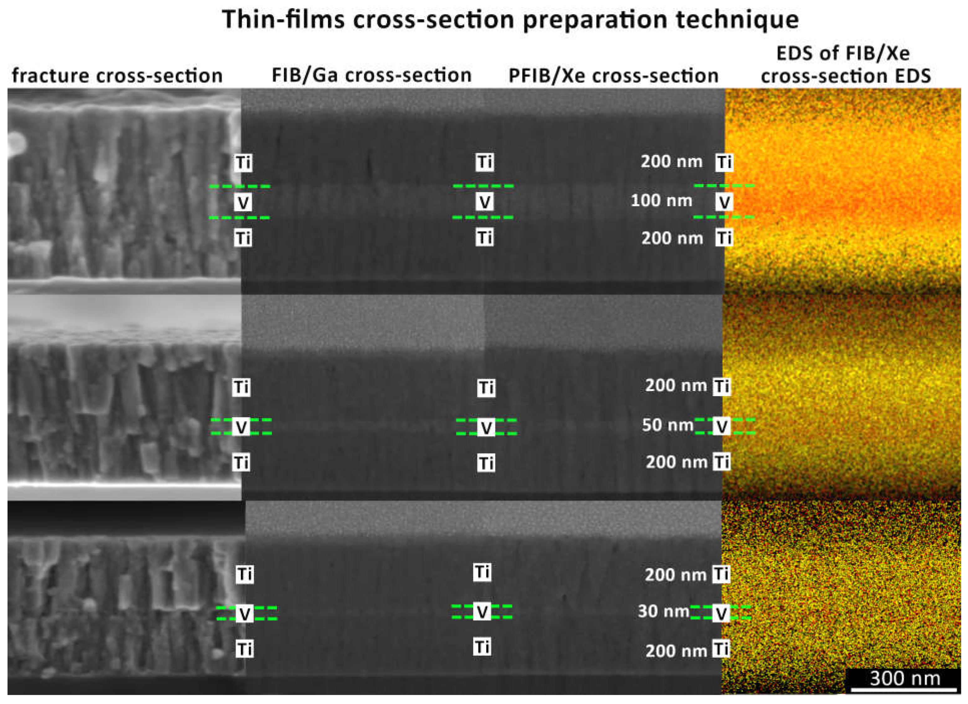
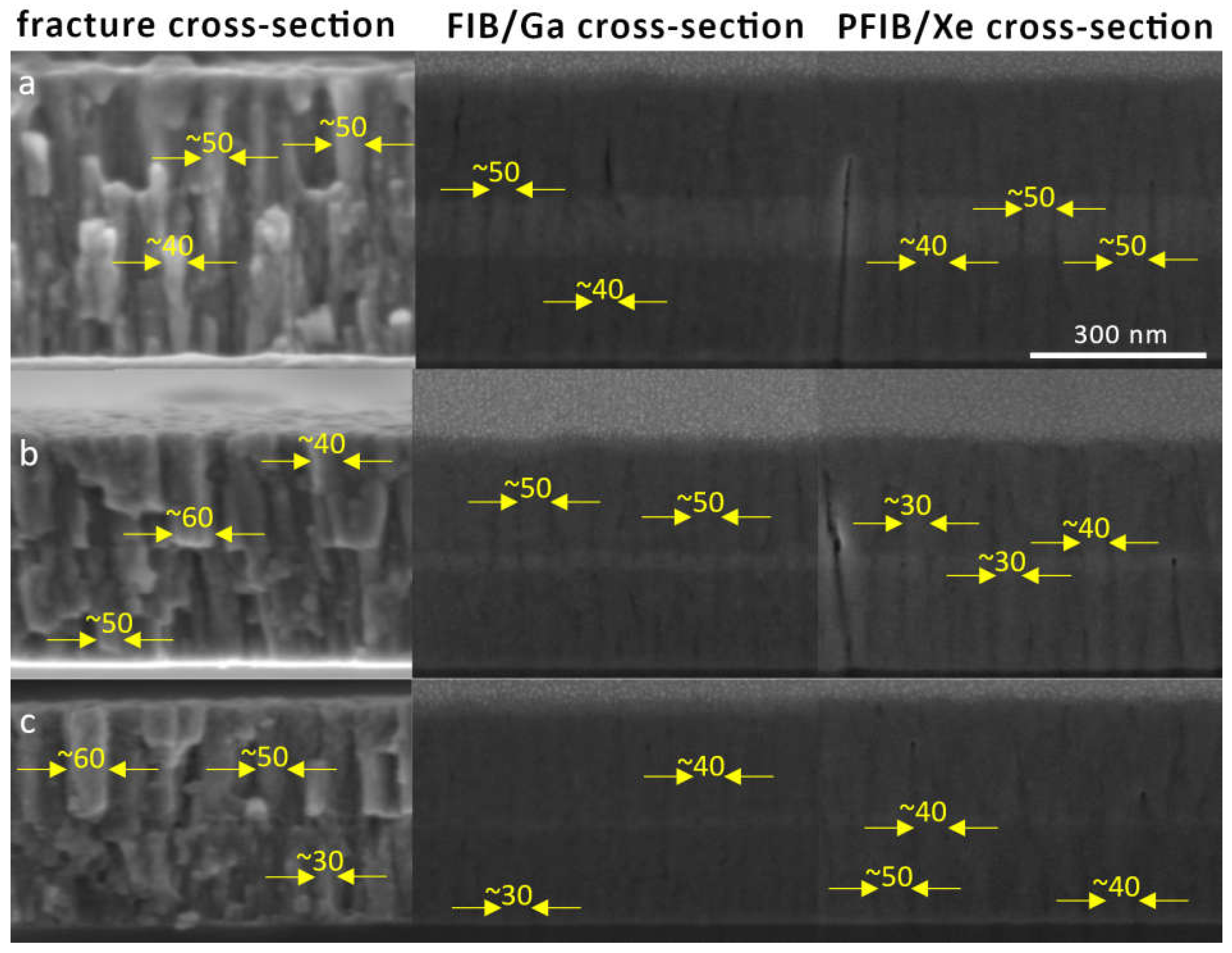
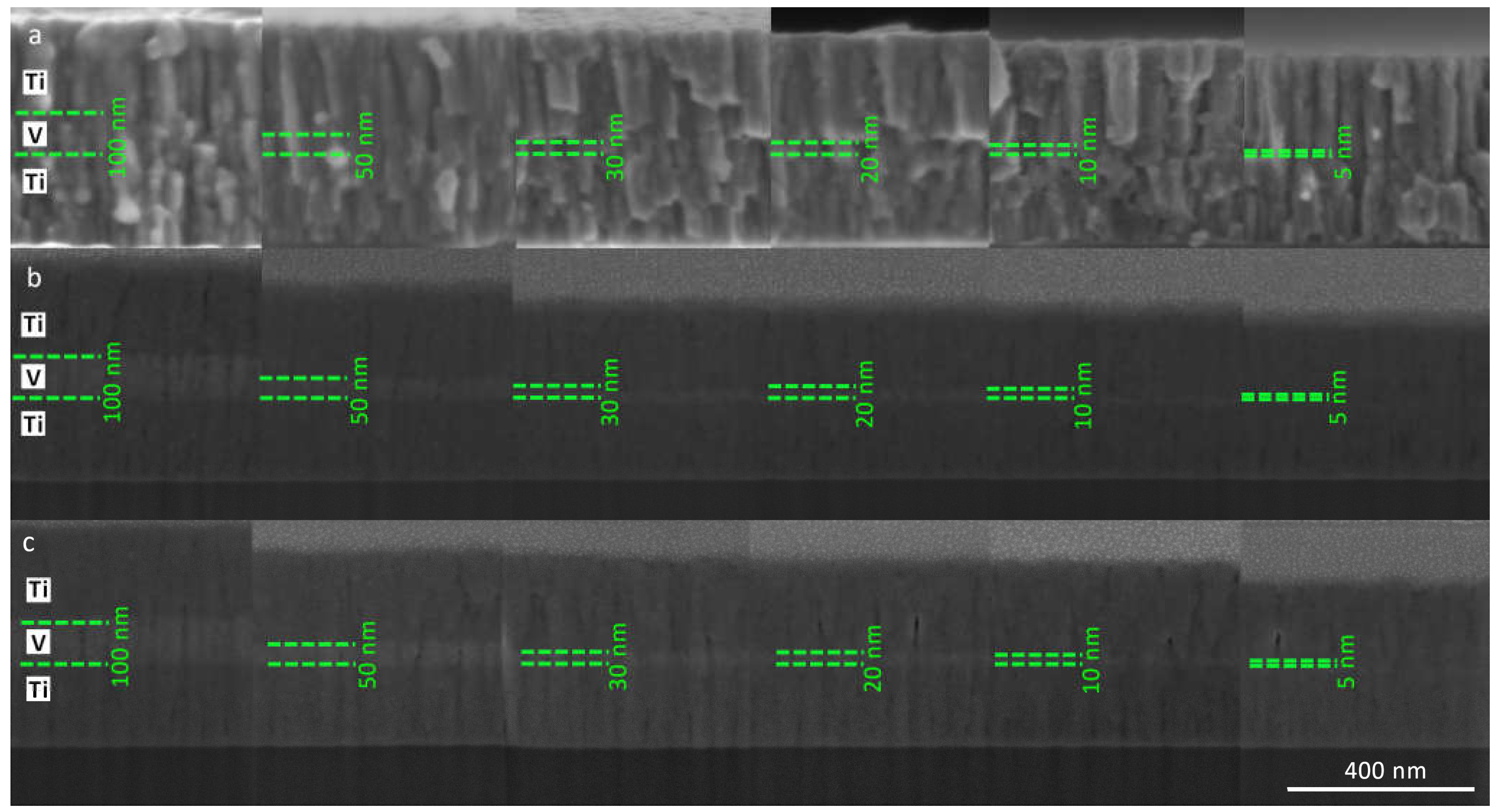
2.3. Preparation Techniques and Details of SEM Measurements
- -
- The preparation of FIB/Ga was carried out with the aid of a Helios NanoLab 600i microscope. Its ion column is equipped in a gallium ion source Ga/LIMS (liquid metal ion source) with the following parameters: (i) current range 0.1–65 nA, (ii) accelerating voltage: 500 V–30 kV. For their microscopic visualization, Helios NanoLab 600i SEM microscope, equipped with a Schottky gun, with a claimed resolution of 1.4 nm @ 1 kV. The imaging was carried out in immersion mode, using a TLD detector, at an acceleration voltage of 2 kV and a current of 0.17 nA.
- -
- The preparation of PFIB/Xe was carried out with the aid of the Helios G4 PFIB CXe microscope. The second source is inductively coupled Xe+ plasma with the following parameters: (i) current range: 1 pA–2.5 uA, (ii) accelerating voltage: 2–30 kV. Its electron column contains a Schottky gun with a claimed resolution of 0.6 nm @ 2–15 kV. Imaging was carried out in immersion mode, using a TLD detector, at an accelerating voltage of 2 kV and a current of 0.1 nA.
3. Results
4. Conclusions
Supplementary Materials
Author Contributions
Funding
Institutional Review Board Statement
Informed Consent Statement
Data Availability Statement
Conflicts of Interest
References
- Ernst, A.; Wie, M.; Aindow, M. A Comparison of Ga FIB and Xe-Plasma FIB of Complex Al Alloys. Microsc. Microanal. 2017, 23 (Suppl. S1), 288–289. [Google Scholar] [CrossRef]
- Lešer, V.; Drobne, D.; Pipan, Ž.; Milani, M.; Tatti, F. Comparison of different preparation methods of biological samples for FIB milling and SEM investigation. J. Microsc. 2009, 233, 309–319. [Google Scholar] [CrossRef] [PubMed]
- Sutton, N.; Hughes, N.; Handley, P. A comparison of conventional SEM techniques, low temperature SEM and the electroscan wet scanning electron microscope to study the structure of a biofilm of Streptococcus crista CR3. J. Appl. Bacteriol. 1994, 76, 448–454. [Google Scholar] [CrossRef]
- Wirth, R. Focused Ion Beam (FIB) combined with SEM and TEM: Advanced analytical tools for studies of chemical composition, microstructure and crystal structure in geomaterials on a nanometre scale. Chem. Geol. 2009, 261, 217–229. [Google Scholar] [CrossRef]
- Kjellsena, K.; Monsøyb, A.; Isachsenb, K.; Detwilerc, R. Preparation of flat-polished specimens for SEM-backscattered electron imaging and X-ray microanalysis—Importance of epoxy impregnation. Cem. Concr. Res. 2003, 33, 611–616. [Google Scholar] [CrossRef]
- Erdman, N.; Campbell, R.; Asahina, S. Precise SEM Cross Section Polishing via Argon Beam Milling. Microsc. Today 2006, 14, 22–25. [Google Scholar] [CrossRef]
- Lee, J.T.Y.; Chow, K. SEM sample preparation for cells on 3D scaffolds by freeze-drying and HMDS. Scanning 2012, 34, 12–25. [Google Scholar] [CrossRef]
- Narbutt, O.; Dąbrowski, H.; Dąbrowska, G. The process of freeze-drying, its wide applications and defense mechanisms against dehydratation. Eduk. Biol. I Sr. 2017, 2, 20–29. [Google Scholar]
- Bassim, N.; De Gregorio, B.; Kilcoyne, A.; Scott, K.; Chou, T.; Wirick, S.; Cody, G.; Stroud, R. Minimizing damage during FIB sample preparation of soft materials. J. Microsc. 2012, 245, 288–301. [Google Scholar] [CrossRef]
- Kim, S.; Park, M.J.; Balsara, N.P.; Liu, G.; Minor, A.M. Minimization of focused ion beam damage in nanostructured polymer thin films. Ultramicroscopy 2011, 111, 191–199. [Google Scholar] [CrossRef]
- Brodusch, N.; Yourdkhani, M.; Hubert, P.; Gauvin, R. Efficient cross-section preparation method for high-resolution imaging of hard polymer composites with a scanning electron microscope. J. Microsc. 2015, 260, 117–124. [Google Scholar] [CrossRef] [PubMed]
- Koh, J.W.; Hwang, G.T.; Hyun, M.S.; Yang, J.; Kim, J.W. Semiconductor layer extraction techniques by SEM. In Proceedings of the 18th IEEE International Symposium on the Physical and Failure Analysis of Integrated Circuits (IPFA), Incheon, Republic of Korea, 4–7 July 2011; pp. 1–3. [Google Scholar]
- Zhang, Y.; Popielarski, B.; Davidson, K.; Men, L.; Zhao, W.; Baumann, F. Development of Ultra-thin TEM Lamella Preparation Technique and Its Application in Failure Analysis. Microsc. Microanal. 2020, 26 (Suppl. S2), 1400–1402. [Google Scholar] [CrossRef]
- Vazdirvanidis, A.; Pantazopoulos, G.; Louvaris, A. Failure analysis of a hardened and tempered structural steel (42CrMo4) bar for automotive applications. Eng. Fail. Anal. 2009, 16, 1033–1038. [Google Scholar] [CrossRef]
- Strecker, A.; Bäder, U.; Kelsch, M.; Salzberger, U.; Sycha, M.; Gao, M.; Richter, G.; van Benthem, K. Progress in the preparation of cross-sectional TEM specimens by ion-beam thinning. Int. J. Mater. Res. 2003, 94, 290–297. [Google Scholar] [CrossRef]
- Abrahams, M.S.; Buiocchi, C.J. Crosssectional specimens for transmission electron microscopy. J. Appl. Phys. 1974, 45, 3315–3316. [Google Scholar] [CrossRef]
- Naito, M.; Yokoyama, T.; Hosokawa, T.; Nogi, K. Nanoparticle Technology Handbook, 3rd ed.; Elsevier: Amsterdam, The Netherlands, 2018. [Google Scholar]
- Contreras, E.; Galindez, Y.; Rodas, M.; Bejarano, G.; Gómez, M. CrVN/TiN nanoscale multilayer coatings deposited by DC unbalanced magnetron sputtering. Surf. Coat. Technol. 2017, 332, 214–222. [Google Scholar] [CrossRef]
- Babaei, K.; Fattah-alhosseini, A.; Elmkhah, H.; Ghomi, H. Surface characterization and electrochemical properties of tantalum nitride (TaN) nanostructured coatings produced by reactive DC magnetron sputtering. Surf. Interfaces 2020, 21, 100685. [Google Scholar] [CrossRef]
- Budak, S.; Xiao, Z.; Johnson, B.; Cole, J.; Drabo, M.; Tramble, A.; Casselberry, C. Highly-Efficient Advanced Thermoelectric Devices from Different Multilayer Thin Films. Am. J. Eng. Appl. Sci. 2016, 9, 356–363. [Google Scholar] [CrossRef]
- Rao, S.G.; Shu, R.; Wang, S.; Boyd, R.; Giuliani, F.; le Febvrier, A.; Eklund, P. Thin film growth and mechanical properties of CrFeCoNi/TiNbZrTa multilayers. Mater. Des. 2022, 224, 111388. [Google Scholar] [CrossRef]
- Aulin, C.; Karabulut, E.; Tran, A.; Wågberg, L.; Lindström, T. Transparent Nanocellulosic Multilayer Thin Films on Polylactic Acid with Tunable Gas Barrier Properties. ACS Appl. Mater. Interfaces 2013, 5, 7352–7359. [Google Scholar] [CrossRef]
- Bartosik, M.; Daniel, R.; Mitterer, C.; Matko, I.; Burghammer, M.; Mayrhofer, P.H.; Keckes, J. Cross-sectional X-ray nanobeam diffraction analysis of a compositionally graded CrNx thin film. Thin Solid Film. 2013, 542, 1–4. [Google Scholar] [CrossRef]
- Parreira, N.M.G.; Polcar, T.; Cavaleiro, A. Characterization of W–O coatings deposited by magnetron sputtering with reactive gas pulsing. Surf. Coat. Technol. 2007, 201, 5481–5486. [Google Scholar] [CrossRef]
- Cavaleiro, A.J.; Santos, R.J.; Ramos, A.S.; Vieira, M.T. In-situ thermal evolution of Ni/Ti multilayer thin films. Intermetallics 2014, 51, 11–17. [Google Scholar] [CrossRef]
- Kang, C.; Huang, H. Mechanical load-induced interfacial failure of a thin film multilayer in nanoscratching and diamond lapping. J. Mater. Process. Technol. 2016, 229, 528–540. [Google Scholar] [CrossRef]
- Kang, C.; Huang, H. A comparative study of conventional and high speed grinding characteristics of a thin film multilayer structure. Precis. Eng. 2017, 50, 222–234. [Google Scholar] [CrossRef]
- Bravman, J.C.; Sinclair, R. The preparation of cross-section specimens for transmission electron microscopy. J. Electron Microsc. Tech. 1984, 1, 53–61. [Google Scholar] [CrossRef]
- Song, K.; Kim, S.G.; Kim, H.J.; Kim, S.K.; Kang, W.K.; Lee, J.C.; Yoon, K.H. Preparation of CuIn1−xGaxSe2 thin films by sputtering and selenization process. Sol. Energy Mater. Sol. Cells 2003, 75, 145–153. [Google Scholar] [CrossRef]
- Wang, Y.; Lin, Z.; Cheng, X.; Xiao, H.; Zhang, F.; Zou, S. Study of HfO2 thin films prepared by electron beam evaporation. Appl. Surf. Sci. 2004, 228, 93–99. [Google Scholar] [CrossRef]
- Santana, A.E.; Karimi, A.; Derflinger, V.H.; Schütze, A. Microstructure and mechanical behavior of TiAlCrN multilayer thin films. Surf. Coat. Technol. 2004, 177–178, 334–340. [Google Scholar] [CrossRef]
- Dieterle, L.; Butz, B.; Müller, E. Optimized Ar+-ion milling procedure for TEM cross-section sample preparation. Ultramicroscopy 2011, 111, 1636–1644. [Google Scholar] [CrossRef]
- Stefenelli, M.; Daniel, R.; Ecker, W.; Kiener, D.; Todt, J.; Zeilinger, A.; Mitterer, C.; Burghammer, M.; Keckes, J. X-ray nanodiffraction reveals stress distribution across an indented multilayered CrN–Cr thin film. Acta Mater. 2015, 85, 24–31. [Google Scholar] [CrossRef]
- Lloyd, G.E. Atomic number and crystallographic contrast images with the SEM: A review of backscattered electron techniques. Mineral. Mag. 1987, 51, 3–19. [Google Scholar] [CrossRef]
- Yamashita, S.; Kikkawa, J.; Yanagisawa, K.; Nagai, T.; Ishizuka, K.; Kimoto, K. Atomic number dependence of Z contrast in scanning transmission electron microscopy. Sci. Rep. 2018, 8, 12325. [Google Scholar] [CrossRef]
- Contreras, E.; Bejarano, G.; Gómez, M. Synthesis and microstructural characterization of nanoscale multilayer TiAlN/TaN coatings deposited by DC magnetron sputtering. Int. J. Adv. Manuf. Technol. 2019, 101, 663–673. [Google Scholar] [CrossRef]
- Riester, M.; Lechner, M.D.; Hilgers, H. Physical vapor-deposited thin hard films on polymers: Sample preparation for SEM analysis. J. Adhes. Sci. Technol. 1999, 13, 963–971. [Google Scholar] [CrossRef]
- Gao, W.; Li, Z. ZnO thin films produced by magnetron sputtering. Ceram. Int. 2004, 30, 1155–1159. [Google Scholar] [CrossRef]
- Wang, C.; Brault, P.; Zaepffel, C.; Thiault, J.; Pineau, A.; Sauvage, T. Deposition and structure of W–Cu multilayer coatings by magnetron sputtering. J. Phys. D: Appl. Phys. 2003, 36, 2709–2713. [Google Scholar] [CrossRef]
- Busch, R.; Tielemann, C.; Reinsch, S.; Müller, R.; Patzig, C.; Krause, M.; Höche, T. Sample preparation for analytical scanning electron microscopy using initial notch sectioning. Micron 2021, 150, 103090. [Google Scholar] [CrossRef] [PubMed]
- Marshall, A.F.; Dobbertin, D.C. Cross-sectioning of layered thin films by ultramicrotomy. Ultramicroscopy 1986, 19, 69–73. [Google Scholar] [CrossRef]
- Becker, O.; Bange, K. Ultramicrotomy: An alternative cross section preparation for oxidic thin films on glass. Ultramicrotomy 1993, 52, 73–84. [Google Scholar] [CrossRef]
- Nguyen, T.D.; Gronsky, R.; Kortright, J.B. Cross-sectional transmission electron microscopy of X-ray multilayer thin film structures. J. Electron Microsc. Tech. 1991, 19, 473–485. [Google Scholar] [CrossRef] [PubMed]
- Sunaoshi, T.; Takeuchi, S.; Kamino, A.; Sasajima, M.; Ito, H. Sample preparation technique for the revelation of a semiconductor dopant using an FE-SEM. In Proceedings of the 2016 IEEE 23rd International Symposium on the Physical and Failure Analysis of Integrated Circuits (IPFA), Singapore, 18–21 July 2016; pp. 148–151. [Google Scholar]
- Reada, J.C.; Braganca, P.M.; Robertson, N.; Childress, J.R. Magnetic degradation of thin film multilayers during ion milling. APL Mater. 2014, 2, 046109. [Google Scholar] [CrossRef]
- Minor, A.M. FIB sample preparation of thin films and soft materials. Microsc. Microanal. 2009, 15 (Suppl. S2), 1544–1545. [Google Scholar] [CrossRef]
- Massl, S.; Thomma, W.; Keckes, J.; Pippan, R. Investigation of fracture properties of magnetron-sputtered TiN films by means of a FIB-based cantilever bending technique. Acta Mater. 2009, 57, 1768–1776. [Google Scholar] [CrossRef]
- Cairney, J.M.; Munroe, P.R.; Hoffman, M. The application of focused ion beam technology to the characterization of coatings. Surf. Coat. Technol. 2005, 198, 165–168. [Google Scholar] [CrossRef]
- Pallecchi, I.; Pellegrino, L.; Bellingeri, E.; Siri, A.S.; Marré, D.; Gazzadi, G.C. Investigation of FIB irradiation damage in La0.7Sr0.3MnO3 thin films. J. Magn. Magn. Mater. 2008, 320, 1945–1951. [Google Scholar] [CrossRef]
- Tanaka, M.; Furuya, K.; Saito, T. TEM observation of FIB induced damages in Ni2Si/Si thin films. Nucl. Instrum. Methods Phys. Res. B 1997, 127–128, 98–101. [Google Scholar] [CrossRef]
- Wojcieszak, D.; Mazur, M.; Kaczmarek, D.; Mazur, P.; Szponar, B.; Domaradzki, J.; Kepinski, L. Influence of the surface properties on bactericidal and fungicidal activity of magnetron sputtered Ti-Ag and Nb-Ag thin films. Mater. Sci. Eng. C 2016, 62, 86–95. [Google Scholar] [CrossRef]
- Mazur, M.; Wojcieszak, D.; Domaradzki, J.; Kaczmarek, D.; Poniedziałek, A.; Domanowski, P. Investigation of microstructure, micro-mechanical and optical properties of HfTiO4 thin films prepared by magnetron co-sputtering. Mater. Res. Bull. 2015, 72, 116–122. [Google Scholar] [CrossRef]
- Mazur, M.; Howind, T.; Gibson, D.; Kaczmarek, D.; Morgiel, J.; Wojcieszak, D.; Zhu, W.; Mazur, P. Modification of various properties of HfO2 thin films obtained by changing magnetron sputtering conditions. Surf. Coat. Technol. 2017, 320, 426–431. [Google Scholar] [CrossRef]
- Mazur, M.; Domaradzki, J.; Wojcieszak, D.; Kaczmarek, D. Investigations of elemental composition and structure evolution in (Ti,Cu)-oxide gradient thin films prepared using (multi)magnetron co-sputtering. Surf. Coat. Technol. 2018, 334, 150–157. [Google Scholar] [CrossRef]
- Adamiak, B.; Wiatrowski, A.; Domaradzki, J.; Kaczmarek, D.; Wojcieszak, D.; Mazur, M. Preparation of multicomponent thin films by magnetron co-sputtering method: The Cu-Ti case study. Vacuum 2019, 161, 419–428. [Google Scholar] [CrossRef]
- Wojcieszak, D.; Mazur, M.; Kaczmarek, D.; Szponar, B.; Grobelny, M.; Kalisz, M.; Pelczarska, A.; Szczygiel, I.; Poniedzialek, A.; Osekowska, M. Structural and surface properties of semitransparent and antibacterial (Cu,Ti,Nb)Ox coating. Appl. Surf. Sci. 2016, 380, 159–164. [Google Scholar] [CrossRef]
- Wojcieszak, D.; Kaczmarek, D.; Antosiak, A.; Mazur, M.; Rybak, Z.; Rusak, A.; Osekowska, M.; Poniedzialek, A.; Gamian, A.; Szponar, B. Influence of Cu-Ti thin film surface properties on antimicrobial activity and viability of living cells. Mater. Sci. Eng. C 2015, 56, 48–56. [Google Scholar] [CrossRef]
- Wojcieszak, D.; Mazur, M.; Kalisz, M.; Grobelny, M. Influence of Cu, Au and Ag on structural and surface properties of bioactive coatings based on titanium. Mater. Sci. Eng. C 2017, 71, 1115–1121. [Google Scholar] [CrossRef]
- Domaradzki, J.; Wiatrowski, A.; Kotwica, T.; Mazur, M. Analysis of electrical properties of forward-to-open (Ti,Cu)Ox memristor rectifier with elemental gradient distribution prepared using (multi)magnetron co-sputtering process. Mater. Sci. Semicond. Process. 2019, 94, 9–14. [Google Scholar] [CrossRef]
- Zhong, X.C.; Wade, A.; Withers, P.J.; Zhou, X.; Cai, C.; Haigh, S.J.; Burke, G.M. Comparing Xe+pFIB and Ga+FIB for TEM sample preparation of Al alloys: Minimising FIB-induced artefacts. J. Microsc. 2021, 282, 101–112. [Google Scholar] [CrossRef]
- Hu, C.; Aindow, M.; Wei, M. Focused ion beam sectioning studies of biomimetic hydroxyapatite coatings on Ti-6Al-4V substrates. Surf. Coat. Technol. 2017, 313, 255–262. [Google Scholar] [CrossRef]
- Burnett, T.L.; Kelley, R.; Winiarski, B.; Contreras, L.; Daly, M.; Gholinia, A.; Burke, M.G.; Withers, P.J. Large volume serial section tomography by Xe Plasma FIB dual beam Microscopy. Ultramicroscopy 2016, 161, 119–129. [Google Scholar] [CrossRef]
- Valdés, M.; Pascual-Winter, M.F.; Bruchhausen, A.; Schreiner, W.; Vázquez, M. Cross-Section Analysis of the Composition of Sprayed Cu2ZnSnS4 Thin Films by XPS, EDS, and Multi-Wavelength Raman Spectroscopy. Phys. Status Solidi 2018, 215, 1800639. [Google Scholar] [CrossRef]
- Giurlani, W.; Enrico Berretti, E.; Lavacchi, A.; Innocenti, M. Thickness determination of metal multilayers by ED-XRF multivariate analysis using Monte Carlo simulated standards. Anal. Chim. Acta 2020, 1130, 72–79. [Google Scholar] [CrossRef]
- Güzelçimen, F. The effect of thickness on surface structure of rf sputtered TiO2 thin films by XPS, SEM/EDS, AFM and SAM. Vacuum 2020, 182, 109766. [Google Scholar] [CrossRef]


| Deposition Parameters of Ti/V/Ti Multilayers | |||||||||
|---|---|---|---|---|---|---|---|---|---|
| PAr [mbar] | Bottom Ti Layer -Target Ti | Middle V Layer -Target V | Top Ti Layer -Target Ti | ||||||
| Power [W] | Time [min.] | t [nm] | Power [W] | Time [min.] | t [nm] | Power [W] | Time [min.] | t [nm] | |
| 1.2 × 10⁻² | 400 | 20 | 200 | 420 | 7 | 100 | 400 | 20 | 200 |
| 3.5 | 50 | ||||||||
| 2 | 30 | ||||||||
| 1.5 | 20 | ||||||||
| 1 | 10 | ||||||||
| 0.5 | 5 | ||||||||
Disclaimer/Publisher’s Note: The statements, opinions and data contained in all publications are solely those of the individual author(s) and contributor(s) and not of MDPI and/or the editor(s). MDPI and/or the editor(s) disclaim responsibility for any injury to people or property resulting from any ideas, methods, instructions or products referred to in the content. |
© 2023 by the authors. Licensee MDPI, Basel, Switzerland. This article is an open access article distributed under the terms and conditions of the Creative Commons Attribution (CC BY) license (https://creativecommons.org/licenses/by/4.0/).
Share and Cite
Sikora, M.; Wojcieszak, D.; Chudzyńska, A.; Zięba, A. Improved Methodology of Cross-Sectional SEM Analysis of Thin-Film Multilayers Prepared by Magnetron Sputtering. Coatings 2023, 13, 316. https://doi.org/10.3390/coatings13020316
Sikora M, Wojcieszak D, Chudzyńska A, Zięba A. Improved Methodology of Cross-Sectional SEM Analysis of Thin-Film Multilayers Prepared by Magnetron Sputtering. Coatings. 2023; 13(2):316. https://doi.org/10.3390/coatings13020316
Chicago/Turabian StyleSikora, Malwina, Damian Wojcieszak, Aleksandra Chudzyńska, and Aneta Zięba. 2023. "Improved Methodology of Cross-Sectional SEM Analysis of Thin-Film Multilayers Prepared by Magnetron Sputtering" Coatings 13, no. 2: 316. https://doi.org/10.3390/coatings13020316
APA StyleSikora, M., Wojcieszak, D., Chudzyńska, A., & Zięba, A. (2023). Improved Methodology of Cross-Sectional SEM Analysis of Thin-Film Multilayers Prepared by Magnetron Sputtering. Coatings, 13(2), 316. https://doi.org/10.3390/coatings13020316