Article

Structural and Mechanical Properties of CrN Thin Films Deposited on Si Substrate by Using Magnetron Techniques

1
Center for Microscopy-Microanalysis and Information Processing, University Politehnica of Bucharest, 060042 Bucharest, Romania
2
MGM Star Construct SRL, 7 Pancota, Str., Building 13, Ap. 19, 02277 Bucharest, Romania
3
Department of Science and Engineering of Oxide Materials and Nanomaterials, Faculty of Chemical Engineering and Biotechnologies, University Politehnica of Bucharest, 060042 Bucharest, Romania
4
Faculty of Electrical Engineering, University Politehnica of Bucharest, 060042 Bucharest, Romania
*
Author to whom correspondence should be addressed.
Coatings 2023, 13(2), 219; https://doi.org/10.3390/coatings13020219
Submission received: 19 October 2022 / Revised: 13 January 2023 / Accepted: 14 January 2023 / Published: 17 January 2023
(This article belongs to the Section Thin Films)

Abstract

:
Chromium nitride thin films are known for their good mechanical properties. We present the characteristics of ultrathin chromium nitride films under 400 nm thickness deposited on silicon substrates by direct current and high-power impulse magnetron sputtering techniques. The methods of investigation of the CrN films were scanning electron microscopy, atomic force microscopy, and nanoindentation. Qualitative and quantitative analyses were performed using AFM and SEM images by fractal dimension, surface roughness and gray-level co-occurrence matrix methods. Our results show that using magnetron techniques, ultrathin CrN films with excellent mechanical properties were obtained, characterized by values of Young’s modulus between 140 GPa and 250 GPa for the samples obtained using high-power impulse magneton sputtering (HiPIMS) and between 240 GPa and 370 GPa for the samples obtained using direct current sputtering (DC). Stiffness measurements also reveal the excellent mechanical properties of the investigated samples, where the samples obtained using HiPIMS sputtering had stiffness values between 125 N/m and 132 N/m and the samples obtained using DC sputtering had stiffness values between 110 N/m and 119 N/m.

1. Introduction

Analyzing the reactivity of transitional metal nitrides, researchers concluded [1,2,3] that nitrides can be produced by the direct action of Nitrogen (N) on the metal when the small N atoms, which satisfy the empirical Hagg rule of the 0.59 ratio between non-metal/metal atom radii [3], will occupy the octahedral spaces in the body-centered cubic (BCC) Chromium (Cr) lattice and that the formed interstitial compound is influenced by the electrons in the metal’s outer shell [1,2]. As such, having five electrons in the three-dimensional shell, Cr will form two nitrides: Chromium nitride (CrN) and Dichromium nitride (Cr2N). The resulting alloy inherits most of the base metal properties. Moreover, metal–nonmetal bonds are formed due to the presence of N atoms in the Cr lattice and the connection is partly ionic due to the difference in electro-negativity between the two elements [4,5]. The resulting CrN has a higher melting point than the base metal, increased hardness, and retains the chemical stability of the base metal [6].
CrN coatings are widespread in applications for protecting surfaces from mechanical and chemical factors with many research articles reporting its properties, especially in tribological applications where because of certain requirements, hard metal coatings with low chemical reactivity must be used [7,8].
CrN was proven as a great option for protective coating applications due to its hardness, low coefficient of friction and great corrosion resistance [9,10,11,12,13,14]. Moreover, CrN exhibits good heat resistance [15,16] and great thermal stability [9,17]. These exceptional properties recommend CrN as a good candidate for microelectronics applications [17], especially in the domain of protection against corrosion, oxidation, and heat [17]. A remarkable property of CrN thin films is the tunability of resistivity with the orientation of crystallites [18], which opens a large palette of electrical applications of CrN.
Supercapacitor applications represent another research area in which massive progress has been made in the last few years [19,20,21,22]. Due to their high specific capacitance and cycling stability, metal nitrides hold great potential as supercapacitor electrode materials. In the Ref. [19] the authors prepared CrN thin films by direct current magnetron (DC) sputtering on polished Si wafers. They found that electrochemical performance can be easily tuned by varying the deposition conditions.
Depositing CrN thin films with thicknesses of tens of nanometers on silicon can be very useful for covering photovoltaic cells [23].
In this article, we deposit CrN thin films on a silicon substrate by using two different techniques and three deposition durations for each technique. Both techniques are methods of physical vapor deposition of thin films onto a substrate, where the main difference is the type of power supply used in the deposition process. The first method, direct current (DC) sputtering, uses a direct current power supply, while the second method, high-power impulse magnetron sputtering (HiPIMS) uses an alternating current power supply. Another difference between the two methods is the quantity that they are able to process; DC sputtering is preferred when dealing with large quantities of large substrates while HiPIMS sputtering is preferred for smaller sized substrates. Both are used as industrial scales, where DC sputtering is used for coating the edge of cutting tools and HiPIMS sputtering is used for the coating of electronic circuits that also act as structural elements. For this reason, we chose to study the structural and mechanical properties of ultrathin CrN depositions, providing insights into the best deposition conditions to a obtain uniform, highly protective coatings. In order to obtain ultrathin coatings, we chose the deposition times of 5, 10, and 15 min, taking into account that in the case of industrial applications, the deposition times typically start from 180 min, for the layers having thicknesses thicker than microns.
The deposition times of 5, 10, and 15 min were chosen specifically because we wanted the deposited layer to be below 400 nm. During our experiments we tested different deposition times, and noticed that for deposition times greater than 15 min, the thickness of the deposited layer would exceed 400 nm. For the research purpose of studying depositions with thicknesses thinner than 400 nm, we chose 15 min as the maximum deposition time, because for this deposition time we would obtain samples with a thickness of the deposited layer near 400 nm. We also chose to produce samples in which the deposited layer was thinner by using the lower deposition times of 5 and 10 min.

2. Materials and Methods

2.1. Sample Preparation

CrN films were deposited using a Z-550-S Leybold–Heraeus (Cologne, Germany) sputtering system. A 6 inch Cr cathode was placed in the top plate of the vacuum chamber and the Silicon (Si) substrates were placed in the bottom holder which is rotating with a speed of 6 rot/min and is kept at a constant temperature of 25 °C. Prior to the deposition, the Si samples were polished and cleaned in Argon plasma for 10 min.
A turbo-molecular pump was used to evacuate the system to a base pressure of 2 × 10⁻⁴ mbar and Argon was released into the chamber at a flow rate of 20 sccm. Separately, N was released into the chamber until a working pressure of 2 × 10⁻² mbar was obtained.
A schematic diagram explaining the deposition chamber can be found in Figure 1.
In the first batch, the power supply for the sputtering system was an SSV-2.5 kW DC power supply, with a constant power of 1000 W, a current of 2.89 A, and a voltage of 392 V. The Si substrate was biased at 100 V, with a frequency of 900 Hz and an impulse duration of 195 μs.
In the second batch, the power supply for the sputtering system was an HiPSTER 1, Ionautics (Linköping, Sweden) high-power impulse magnetron sputtering (HiPIMS) power supply, with an average power of 1000 W, frequency of 900 Hz, with an impulse duration of 65 μs. The substrate was biased at 100V, with a frequency of 900 Hz and an impulse duration of 195 μs.
A list of the samples is found in Table 1, embracing their designations, the power supply type, and the deposition time.

2.2. Characterisation Techniques

To determine the film morphology and thickness and the chemical composition of both the CrN layer and the Si substrate, a high-resolution scanning electron microscope of the Inspect F50, FEI (Hillsboro, OR, USA, with field emission electron gun–FEG) equipped with an EDAX-type energy-dispersive X-ray spectrometer (EDAX) was used.
For the investigations of surface topography, an NX10 Park (Suwon, Republic of Korea) Atomic Force Microscope (AFM) was used, equipped with a non-contact probe (NCHR, Nanosensors, Neuchatel, Switzerland) with a resonance frequency of 300 kHz and a sub-10 nm tip radius. We acquired 512 × 512 pixel images on 10 × 10 µm2 areas on the deposited films, and we further used the images for the quantitative measurements.
On the same AFM system, we performed elasticity measurements by force–distance spectroscopy, for which we used a contact probe (CONTSCR, Nanosensors, Neuchatel, Switzerland) with a tip radius of sub-10 nm and a force constant of 0.2 N/m. We computed Young’s modulus with the Hertzian method using the resulting force-separation curves.
Shallow nanoindentation was performed as well by using the AFM system with a TD26706 probe (Micro Star Technology, Huntsville, AL, USA) having a nominal force constant of 154 N/m, resonant frequency of 40 kHz, and a tip radius smaller than 25 nm. Analysis of the approach–retract curves in the shallow regime was used to extract the material stiffness.
Water contact angle tests were performed using a simple imaging system built on table composed by a CCD camera and an adjustable microscope sample holder. For each sample, a drop of 10 μL demineralized water was placed on the surface and imaged by our system. The acquired images were analyzed using ImageJ to measure the contact angle.

2.3. Image Analysis and Measurements

We used both acquired SEM and AFM images for quantitative and qualitative measurements. Being one of the crucial technical parameters of the manufactured parts, especially in metallic deposition applications, surface roughness was one of the quantities evaluated from the AFM investigations. As a measure of surface roughness, we used the surface area roughness (Sq) present in the AFM surface topography. We evaluated the surface roughness by using Gwyddion image analysis software [17].
The fractal dimension (FD) is another measure used to quantify the organization of structures appearing in a microscopic image. FDs values close to 2 indicate smoother surfaces, and values close to 3 indicate a high degree of roughness. Fractal analysis can be performed either on grayscale images or binary (black and white) images. In the case of the analysis carried out on samples within the experiment, we considered the case of grayscale images. We performed fractal analysis by using ImageJ’s FracLac plugin (2015Apra4308, 2015, Audrey Karperien, Bathurst, Australia), which computes the fractal dimension using the “box counting” method. With this method, the image is covered by successively smaller squares. At each step, the number of squares containing the image elements is counted. Such image elements are different in pixel intensity in the area occupied by the squares. The fractal dimension, which is a measure of the complexity of the image, is calculated as the slope of the regression line of the log–log plot of the difference in pixel intensity in the area covered by the squares and the size of the squares.
The other two measures of uniformity in an image are entropy (S) and autocorrelation length (L). The entropy reflects the uniformity of the height distribution of the topographical profile [18], while the autocorrelation length offers a measure of the uniformity of the surface texture [19,20]. We computed these two parameters using Gwyddion (2.62, 2022, Czech Metrology Institute, Jihlava, Czech Republic).
Another set of quantitative measurements can be obtained from the gray-level co-occurrence matrix (GLCM) which represents a second-order statistical modality that provides information related to the spatial relationship between pixel intensities in each image [21]. The GLCM matrix is built based on the number of occurrences of a certain pair of pixels, at a specific distance between pixels. Each result is divided by the total number of elements to calculate a probability. Such a matrix can be calculated for any distance between pixels, either horizontally (0°), vertically (90°), or diagonally (45°, 135°). Because we observed only small variations between the values calculated according to different orientations, we report here the average value for the results obtained for the four orientations. We extract two features of the GLCM: energy (or the angular second moment) and correlation.

3. Results and Discussions

3.1. Chemical Composition

EDAX elemental mapping obtained for the case of DC power supply deposition are presented in Figure 2. For each time duration of the deposition, a composite image is displayed containing a SEM cross-section and Si, Cr, and N elemental maps, respectively.
Figure 3 presents the EDAX elemental mapping obtained for the case of HiPIMS power supply deposition. Similar to the previous case, for each time duration of the deposition a composite image is displayed containing a SEM cross-section and Si, Cr, and N elemental maps, respectively.
The distribution of Cr and N in the deposited layer (Figure 2 and Figure 3) is homogeneous and uniform with no noticeable defects in the deposition layer. It is therefore expected that the thin CrN layer will provide corrosion resistance for the Si surface beneath. The interaction (diffusion) at the deposition/substrate interface can also be noticed.
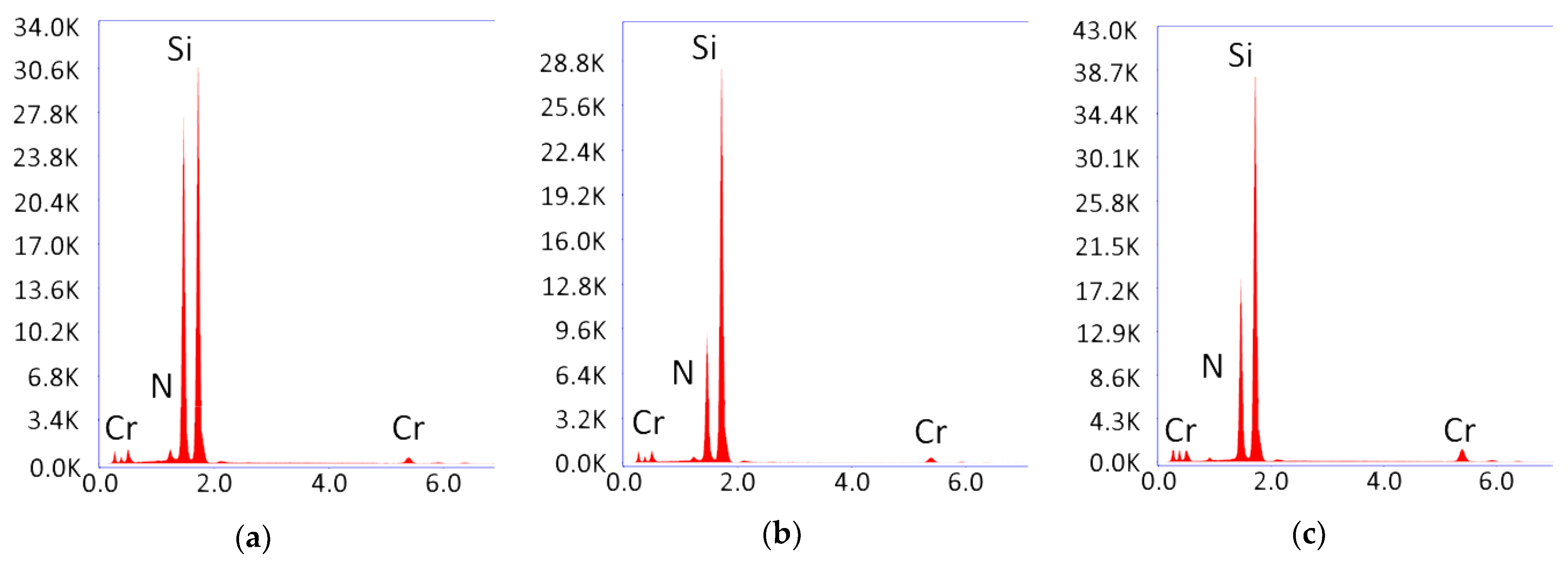
Apart from a qualitative inspection, EDAX spectra allow the measurement of the weight distribution of each element: Si (substrate), Cr, and N. The EDAX spectra for each sample was acquired in the region of the red boxes represented in Figure 2 and Figure 3. The corresponding spectra (number of counts vs. energy levels) for the CrN films deposited by the DC power supply for each time duration are presented in Figure 4.
Similar to the previous case, the corresponding spectra (number of counts vs. energy levels) for the CrN films deposited by the HiPIMS power supply for each time duration are presented in Figure 5.
The existence of Cr and N signals in the EDAX spectra (Figure 4 and Figure 5) confirms the successful deposition of an ultrathin CrN layer on the Si substrate. The strong presence of Si signals in the EDAX spectra represented in both Figure 4 and Figure 5 is explained by the dimensions of the boxes chosen for analysis (represented in Figure 2 and Figure 3 as red boxes). Even if the analysis area was only positioned on the upper position of the deposited layer there would still be a Si signal in the EDAX spectra due to electron scattering in the ultrathin CrN layer.

3.2. SEM Investigations

3.2.1. Surface Morphology

The surface morphology imaged by SEM for the case of the DC power supply is represented below (Figure 6), for the three durations: 5 (Figure 6a), 10 (Figure 6b), and 15 (Figure 6c) min.
Similarly, the morphology analysis results for the case of the HiPIMS power supply are represented in Figure 7, for the same time durations of the deposition process (5, 10, and 15 min, respectively).
All the images in Figure 6 and Figure 7 were obtained with the same magnification.
For the DC power supply (Figure 6), the deposition was rough, and a fine columnar growth pattern could be seen even after a deposition time of 5 min. The growth pattern for the DC method first develops as small blobs, and as the deposition time increases those blobs act as nuclei for other blobs to form near and on top, thus increasing in size. Finally, because of the distribution of these blobs, a columnar growth pattern begins to form. Our findings are confirmed by other results in the literature, as DC sputtering is known to create fine and columnar depositions, a fact which we have shown holds true even for ultrathin deposition as in our case. On the contrary, in the case of the HiPIMS power supply (Figure 7), no noticeable growth pattern can be distinguished. This shows that the deposition layer is smooth and homogeneous as there are no noticeable growth patterns. This kind of deposition mechanism is also representative, as the HiPIMS deposition is known to create dense and glassy depositions. This seems to hold even for ultrathin depositions, as in our case.

3.2.2. Surface Morphology Analysis

The above morphology images obtained by SEM investigations were further analyzed to compute the FD parameter for each sample. Table 2 summarizes the results of this analysis.
The fractal dimension values in Table 2 show the common behavior of the samples irrespective of the power supply or the deposition time, varying between 2.696 for the CrNHi5 sample and 2.832 for the CrNDC5 sample.
The same morphology images were also analyzed from a statistical point of view. After computing the GLCM matrix for each image, the energy and correlation parameters were extracted for different pixel distances (1, 10, and 100 pixels) in each image. The results are summarized in Table 3.
The energy values of the surface morphology GLCM matrix (Table 3) did not have great variations based on the pixel distance, but they did vary based on power supply type and deposition time. For the DC power supply, the energy increases with deposition time and for the HiPIMS power supply, the energy decreases with deposition time. This means that the layer deposited using the DC power supply becomes smoother as the deposition time increases, while the layer deposited using the HiPIMS power supply becomes rougher.
For the correlation value extracted from the surface morphology GLCM matrix (Table 3), we notice a dependency on three factors: pixel distance, power supply type, and deposition time. Correlation greatly decreases with pixel distance. For both the DC and HiPIMS power supplies, the correlation increases with deposition time. An interesting aspect is the rate at which correlation increases, where the correlation for the deposition performed using the DC power supply starts at 0.033 for the distance of 1 pixel and after 15 min it ends at 0.085, while the correlation for the deposition done using the HiPIMS power supply starts at a greater value of 0.064 for the distance of 1 pixel, and after 15 min it ends at 0.067. Thus, even if the correlation parameter for the HiPIMS power supply starts at a greater value because the correlation for the DC power supply increases at a greater rate, it ends up being smaller than the correlation for the DC power supply.

3.2.3. Film Thickness

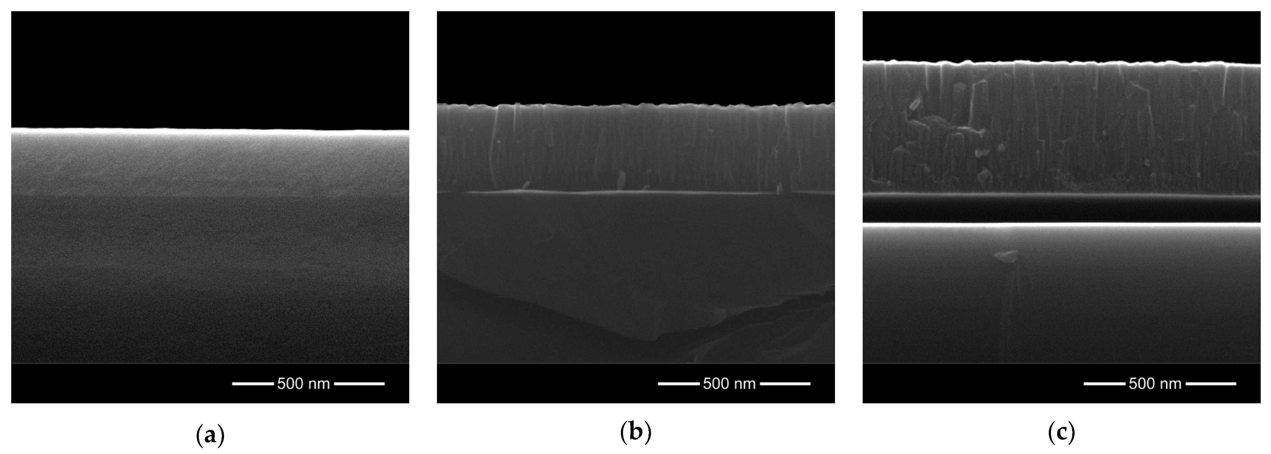
Measurements for the thickness of the CrN layer performed by SEM are presented below for the case of the DC power supply (Figure 8).
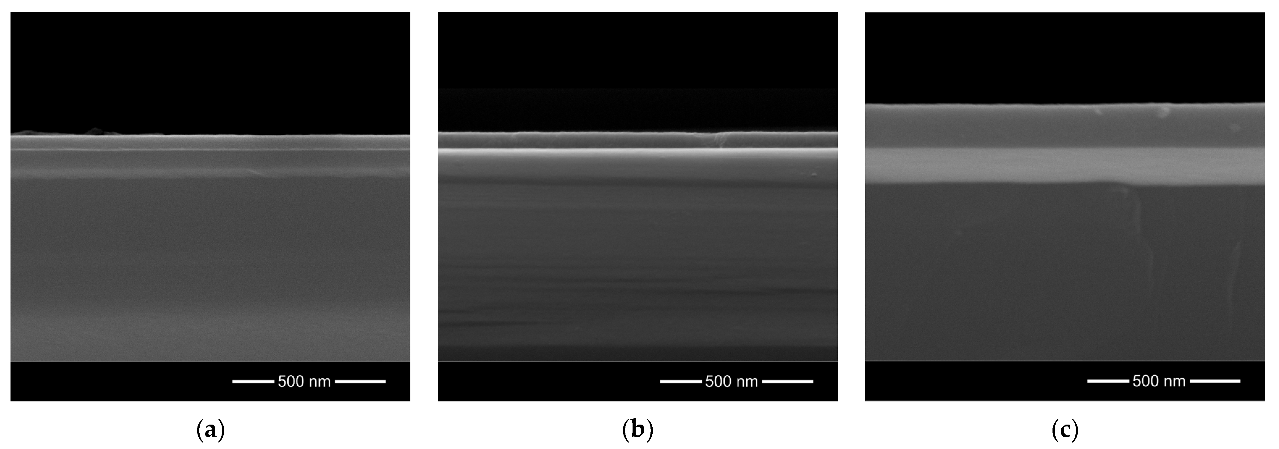
Similarly, the corresponding images for thickness measurements of the deposited film for the case of HiPIMS power supply are represented in Figure 9. The same magnification factor was used in all displayed SEM investigations to aid the visual perception.
Table 4 summarizes the measured thickness for each presented sample.
Analyzing Figure 8 and Figure 9, one can notice that the main difference in the films deposited by DC sputtering and HiPIMS sputtering consists greatly in the structure of the morphology. In Figure 8, the deposited layer when using the DC power supply seems fine and has a columnar structure, while in Figure 9, the deposited layer in the case of the HiPIMS power supply seems dense and uniform. Moreover, the film thickness can be extracted from the figures mentioned previously. When using the DC power supply, the film thickness increases at an approximately constant rate, but when using the HiPIMS power supply the film thicknesses for the deposition times of 5 and 10 min are approximately the same, while for the deposition time of 15 min it sees a sudden jump of 200%.
The thickness measurements also confirm the differences in material quantity deposited by the two methods, which resulted from the chemical composition analysis. For each time deposition duration, the CrN layer is 4 to above 5 times thicker in the case of the DC power supply than in the case of HiPIMS.

3.3. AFM Investigations

3.3.1. Surface Topography

The topography images obtained by AFM investigations on samples containing CrN films deposited by the DC power supply are presented in Figure 10.
Figure 11 shows the topography images obtained by AFM investigations on samples containing CrN films deposited by the HiPIMS power supply.
Analysis of the topography images acquired on samples obtained by the DC sputtering method (Figure 10) reveals that the defects tend to be visible at reduced deposition times, with the characteristic structures of the substrate fading out after a deposition time of 10 min. Another noticeable observation is that in DC sputtering, a characteristic columnar growth structure is observed. Even after 15 min of deposition, the CrN layer does not become uniform.
The results obtained by AFM imaging of the CrN layer deposited through HiPIMS sputtering (Figure 11) indicate that at reduced deposition times the microscopic scratches that were on the Si substrate took place are still visible after the deposition process, indicating an ultrathin layer (which is confirmed by the results from Table 4). As the deposition time increases to 10 min, the microscopic scratches that were on the Si substrate are still visible, indicating the formation of a layer that has a thickness comparable to the layer deposited in 5 min. Lastly, for the deposition time of 15 min, the HiPIMS sputtering method creates a layer that has a more uniform appearance than those obtained at shorter deposition times. The same conclusion is supported by the statistical analysis discussed below.

3.3.2. Mechanic (Elastic) Properties

We compute Young’s modulus from force–distance curve analysis performed in 15 different locations for each sample. Similarly, we determine the surface stiffness as the slope of the force-separation curve in the contact region from approach–retract curves resulting from nanoindentation processes. The results can be found in Table 5.
For both DC and HiPIMS methods, there is a decreasing trend of Young’s modulus with the deposition time. This trend appears due to the measurement method, which is highly dependent on the tip-surface interaction. Consequently, the decrease of the Young’s modulus has different explanations depending on the power supply. For DC power supply, the columnar deposition which is gradually formed with the increase of the time deposition strongly influences the tip-sample interaction due to holes created between the columns. Therefore, the measured Young’s modulus decreases because of this columnar character of the films. On the other hand, in the case of the HiPIMS power supply the films are very thin and the interaction between tip and the sample surface is strongly influenced by the substrate.
Young’s modulus depends as well on the power supply type. The values for the DC power supply are always higher, for the same deposition time, than the values for the HiPIMS power supply.
For the stiffness, one can notice higher values in the case of films obtained by the HiPIMS power supply than those for films obtained by DC sputtering, for the same deposition time. There is also an increasing trend with the deposition time, which is an expected outcome.
For Dc power supply, the columnar deposition strongly influences the tip-sample interaction due to holes created between the columns. The AFM tip disrupts the deposited columns easier when they are longer (for higher deposition times) and as a consequence the measures Young’s modulus decreases with time deposition (Figure 12). For the HiPIMS power supply, the CrN deposition is very thin and takes the form of a uniform film. Therefore (Figure 13), in this case the Young’s modulus measurement is highly influenced by the substrate.

3.3.3. Surface Topography Analysis

The statistical parameters extracted from the surface topography images were roughness (Rq), fractal dimension (FD), entropy (S), and autocorrelation length (L). The values resulting from this analysis of all the samples are summarized in Table 6.
The surface roughness analysis (Table 6) shows that although both DC and HiPIMS generally result in sub-1 nm surface roughness, in the HiPIMS method the highest sur-face roughness recorded was 0.603 nm, which is 1.7 times less than the highest surface roughness recorded with the DC method. It is worth discussing here the increased rate of surface roughness depending on the power supply method. For both methods, it can be observed a non-linear increase of roughness with time deposition. For DC method the roughness tends to increase rapidly after 5 to 10 min of deposition time (29% increase) and slower after another 5 min (13% increase in the interval between 10 to 15 min deposition time). On the other hand, for the HiPIMS method, we observe a slow increase of the roughness between 5- and 10-min deposition time (13%) and a rapid increase of the roughness between 10- and 15-min deposition time (24%).
For the fractal dimension, there is an increasing trend with deposition time regardless of the power supply type used. While the increase of the fractal dimension is non-linear with time deposition, the fractal dimension increases slowly between 5 to 10 min and much faster between 10 to 15 min of deposition time, for both methods. Regarding the entropy values (Table 6) there is no easily discernable dependency in either deposition time or power supply used. This means that the uniformity of the height distribution remains nearly constant regardless of the power supply or time deposition. For the autocorrelation length, there is a decreasing trend with the increase of deposition time, which means that the uniformity of surface texture is highly dependent on the time deposition.
After GLCM analysis the interest parameters (energy and correlation) were extracted and summarized in Table 7. Both energy and correlation were extracted at three different pixel distances (1, 10, and 100).
In the data summarized in Table 7, we can notice a decreasing trend, both with the pixel distance and with deposition time. This means that as deposition time and pixel distance increase the texture of the deposited layer becomes less uniform, regardless of power supply type used.
The same is not true for the correlation values of the AFM topography GLCM matrix, where we see an increasing trend with deposition time but a decreasing trend with pixel distance.

3.4. Water Contact Angle

The surface wettability of the samples was tested by performing water contact angle measurements, as described in the Methods section. The purpose was to evaluate the protective capability of the deposited CrN layers, which means that the surface must exhibit hydrophobic properties (contact angles > 90°). Such a surface will prevent water infiltrations and will have self-cleaning behavior as well. Figure 14 shows the results obtained on the samples deposited by use of thenDC power method for each deposition time. It can be observed that for the 5- and 10-min deposition the surface is hydrophobic (contact angles of 99.5° and 98.2°, respectively), while for the 15 min deposition the surface is almost hydrophobic (contact angle of 88.9°). Interestingly, the contact angle decreases with the increase of the CrN layer thickness.
For the HiPIMS power supply, similar results were obtained. For 5- and 10-min deposition the contact angle is 98.5° and 95.2° respectively. For the case of 15 min deposition time the contact angle is 89.5°, which is a limit case, close to the hydrophobicity condition. The results are displayed in Figure 15. Similar to the DC power supply case, the contact angle decreases with the increase of the deposited layer thickness. This means that the interface between Si substrate and the CrN layer plays a key role in the resulted wettability property of the surface.

4. Conclusions

We investigated the thin CrN films deposited on silicon by using two different methods and for three durations of time deposition, and we found important qualitative and quantitative changes in the properties of the deposited layer. Columnar and fine structures were noticed in the cross-sections depending on the type of power supply used. The surface of the deposited films changed and became smooth and homogeneous for the HiPIMS power supply, but rough and with noticeable growth patterns for the DC power supply.
We observed both qualitative and quantitative changes in the fractal dimension, roughness values, autocorrelation length, Young’s modulus, and stiffness value. All these measures are dependent on both the deposition time and the type of power supply used.

Author Contributions

Conceptualization, S.G.S. and G.A.S.; Data curation, D.E.T., S.R.A. and S.G.S.; Formal analysis, D.E.T., S.R.A. and E.V.; Funding acquisition, A.S., G.A.S. and C.K.B.; Investigation, D.E.T., S.R.A., E.F., E.V. and D.C.; Methodology, G.A.S.; Project administration, G.A.S.; Resources, A.S., G.A.S. and C.K.B.; Software, D.E.T., R.H. and S.R.A.; Supervision, G.A.S.; Validation, G.A.S.; Writing–original draft, D.E.T., S.R.A. and D.C.; Writing–review & editing, D.E.T., R.H., S.R.A., S.G.S. and G.A.S. All authors have read and agreed to the published version of the manuscript.

Funding

This research was funded by The Ministry of Education and Research, as the Intermediate Body for the Program Operational Competitiveness 2014–2020, project „Innovative technologies for physical vacuum deposition based on thin layers, multifunctional, nanostructured intended for large parts–LargCoat”, MySMIS 2014+: 122543.

Institutional Review Board Statement

Not applicable.

Informed Consent Statement

Not applicable.

Data Availability Statement

Not applicable.

Conflicts of Interest

The authors declare no conflict of interest.

References

  1. Robert Odette, G.; Cunningham, N.J.; Stan, T.; Ershadul Alam, M.; de Carlan, Y. Nano-Oxide Dispersion-Strengthened Steels. In Structural Alloys for Nuclear Energy Applications; Robert Odette, G., Zinkle, S.J., Eds.; Elsevier: Amsterdam, The Netherlands, 2019; pp. 529–583. [Google Scholar]
  2. Glasson, D.R.; Jayaweera, S.A.A. Formation and Reactivity of Nitrides I. Review and Introduction. J. Appl. Chem. 1968, 18, 65–77. [Google Scholar] [CrossRef]
  3. Eklund, P.; Kerdsongpanya, S.; Alling, B. Transition-Metal-Nitride-Based Thin Films as Novel Energy Harvesting Materials. J Mater. Chem. C Mater. 2016, 4, 3905–3914. [Google Scholar] [CrossRef] [Green Version]
  4. Barata, A.; Cunha, L.; Moura, C. Characterisation of Chromium Nitride Films Produced by PVD Techniques. Thin Solid Film. 2001, 398–399, 501–506. [Google Scholar] [CrossRef] [Green Version]
  5. Sanjinés, R.; Hones, P.; Lévy, F. Hexagonal Nitride Coatings: Electronic and Mechanical Properties of V2N, Cr2N and δ-MoN. Thin Solid Film. 1998, 332, 225–229. [Google Scholar] [CrossRef]
  6. Lin, J.; Moore, J.J.; Sproul, W.D.; Mishra, B.; Wu, Z.; Wang, J. The Structure and Properties of Chromium Nitride Coatings Deposited Using Dc, Pulsed Dc and Modulated Pulse Power Magnetron Sputtering. Surf. Coat Technol. 2010, 204, 2230–2239. [Google Scholar] [CrossRef]
  7. Ahn, S.H.; Choi, Y.S.; Kim, J.G.; Han, J.G. A Study on Corrosion Resistance Characteristics of PVD Cr-N Coated Steels by Electrochemical Method. Surf. Coat Technol. 2002, 150, 319–326. [Google Scholar] [CrossRef]
  8. Liu, C.; Bi, Q.; Matthews, A. EIS Comparison on Corrosion Performance of PVD TiN and CrN Coated Mild Steel in 0.5 N NaCl Aqueous Solution. Corros. Sci. 2001, 43, 1953–1961. [Google Scholar] [CrossRef]
  9. Zhou, L.; Körmann, F.; Holec, D.; Bartosik, M.; Grabowski, B.; Neugebauer, J.; Mayrhofer, P.H. Structural Stability and Thermodynamics of CrN Magnetic Phases from Ab Initio Calculations and Experiment. Phys. Rev. B Condens. Matter Mater. Phys. 2014, 90, 184102. [Google Scholar] [CrossRef] [Green Version]
  10. Abdallah, B.; Kakhia, M.; Alssadat, W.; Zetoun, W. Study of Power Effect on Structural, Mechanical Properties and Corrosion Behavior of CrN Thin Films Deposited by Magnetron Sputtering. Prot. Met. Phys. Chem. Surf. 2021, 57, 80–87. [Google Scholar] [CrossRef]
  11. Marulanda, D.M.; Olaya, J.J.; Patino, E.J. Evaluation of Electrical Properties of Cr/CrN Nano-Multilayers for Electronic Applications. J. Nanosci. Nanotechnol. 2011, 11, 5418–5422. [Google Scholar] [CrossRef]
  12. Cunha, L.; Andritschky, M.; Pischow, K.; Wang, Z. Microstructure of CrN Coatings Produced by PVD Techniques. Thin Solid Film. 1999, 355–356, 465–471. [Google Scholar] [CrossRef]
  13. Nouveau, C.; Djouadi, M.A.; Djouadi, M.A.; Banakh, O.; Sanjinés, R.; Lévy, F. Stress and Structure Profiles for Chromium Nitride Coatings Deposited by r.f. Magnetron Sputtering. Thin Solid Film. 2001, 398–399, 490–495. [Google Scholar] [CrossRef]
  14. Gilewicz, A.; Chmielewska, P.; Murzynski, D.; Dobruchowska, E.; Warcholinski, B. Corrosion Resistance of CrN and CrCN/CrN Coatings Deposited Using Cathodic Arc Evaporation in Ringer’s and Hank’s Solutions. Surf. Coat Technol. 2016, 299, 7–14. [Google Scholar] [CrossRef]
  15. Montemor, M.F. Functional and Smart Coatings for Corrosion Protection: A Review of Recent Advances. Surf Coat Technol 2014, 258, 17–37. [Google Scholar] [CrossRef]
  16. Aperador, W.; Duque, J.; Delgado, E. Electrochemical and Tribological and Mechanical Performances Coatings Multilayer Type NbC/CrN. Int. J. Electrochem. Sci. 2016, 11, 6347–6355. [Google Scholar] [CrossRef]
  17. Hultman, L. Thermal Stability of Nitride Thin Films. Vacuum 2000, 57, 1–30. [Google Scholar] [CrossRef]
  18. Muhammed Sabeer, N.A.; Pradyumnan, P.P. Augmentation of Thermoelectric Power Factor of P-Type Chromium Nitride Thin Films for Device Applications. Mater. Sci. Eng. B 2021, 273, 115428. [Google Scholar] [CrossRef]
  19. Wei, B.; Liang, H.; Zhang, D.; Wu, Z.; Qi, Z.; Wang, Z. CrN Thin Films Prepared by Reactive DC Magnetron Sputtering for Symmetric Supercapacitors. J. Mater. Chem. A Mater. 2017, 5, 2844–2851. [Google Scholar] [CrossRef]
  20. Zhu, M.; Huang, Y.; Huang, Y.; Li, H.; Wang, Z.; Pei, Z.; Xue, Q.; Geng, H.; Zhi, C. A Highly Durable, Transferable, and Substrate-Versatile High-Performance All-Polymer Micro-Supercapacitor with Plug-and-Play Function. Adv. Mater. 2017, 29, 1605137. [Google Scholar] [CrossRef]
  21. Liu, C.F.; Liu, Y.C.; Yi, T.Y.; Hu, C.C. Carbon Materials for High-Voltage Supercapacitors. Carbon N. Y. 2019, 145, 529–548. [Google Scholar] [CrossRef]
  22. Arif, M.; Sanger, A.; Singh, A. Sputter Deposited Chromium Nitride Thin Electrodes for Supercapacitor Applications. Mater. Lett. 2018, 220, 213–217. [Google Scholar] [CrossRef]
  23. Büldt, L.A.; Wenger, O.S. Chromium Complexes for Luminescence, Solar Cells, Photoredox Catalysis, Upconversion, and Phototriggered NO Release. Chem. Sci. 2017, 8, 7359–7367. [Google Scholar] [CrossRef] [PubMed]
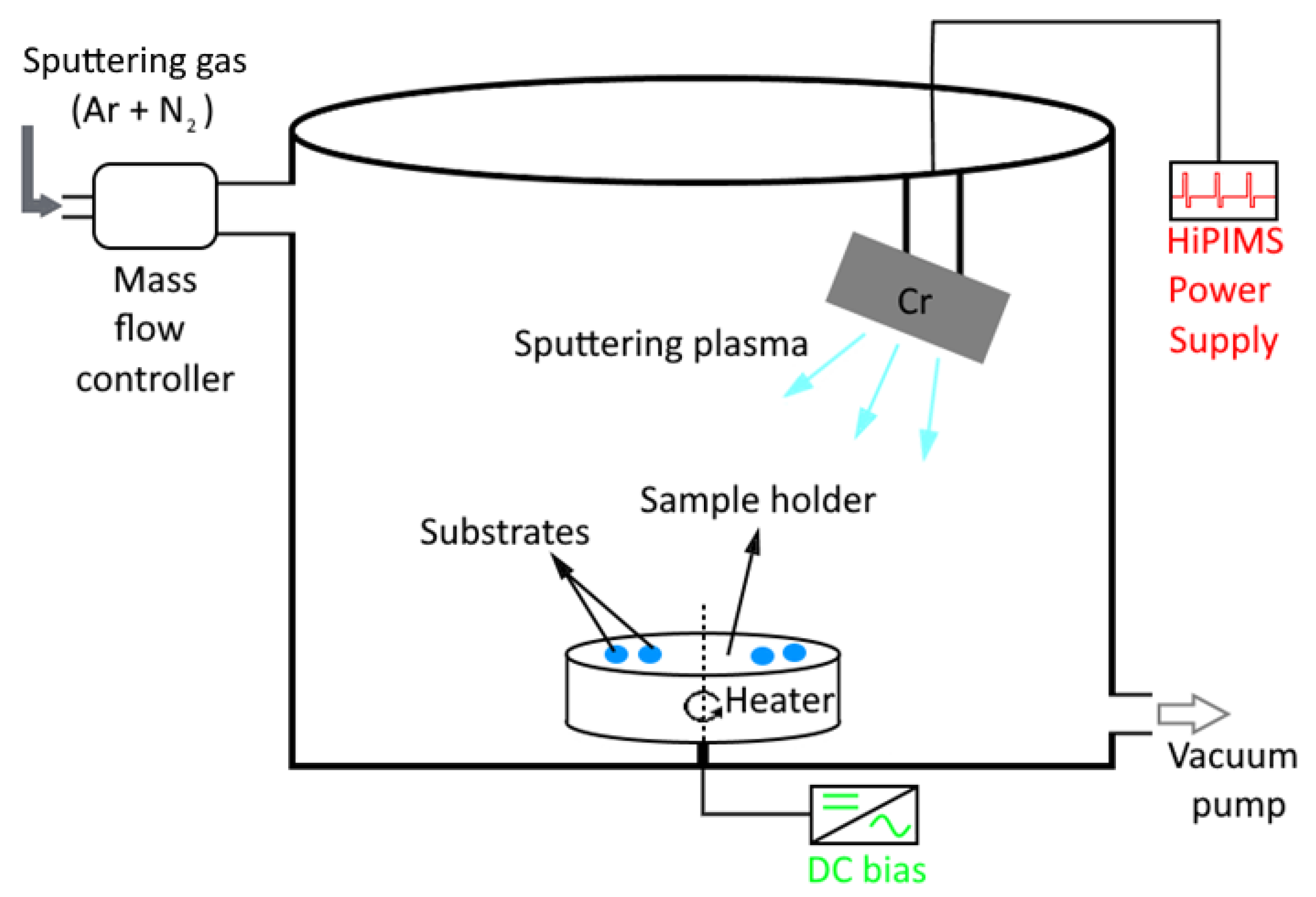
Figure 1. The general schematic diagram explaining the deposition chamber.
Coatings 13 00219 g001
Figure 2. EDAX elemental mapping showing the distribution of chemical elements using the DC power supply for the deposition times of (a) 5 min, (b) 10 min, and (c) 15 min.
Coatings 13 00219 g002
Figure 3. EDAX elemental mapping showing the distribution of chemical elements using the HiPIMS power supply for the deposition times of (a) 5 min, (b) 10 min, and (c) 15 min.
Coatings 13 00219 g003
Figure 4. EDAX spectrum (number of counts vs. energy levels) when using the DC power supply for the deposition times of (a) 5 min, (b) 10 min, and (c) 15 min.
Coatings 13 00219 g004
Figure 5. EDAX spectrum (number of counts vs. energy levels) when using the HiPIMS power supply for the deposition times of (a) 5 min, (b) 10 min, and (c) 15 min.
Coatings 13 00219 g005
Figure 6. Surface morphology of the deposited layer when using the DC power supply and for the deposition times of (a) 5 min, (b) 10 min, and (c) 15 min.
Coatings 13 00219 g006
Figure 7. Surface morphology of the deposited layer when using the HiPIMS power supply and for the deposition times of (a) 5 min, (b) 10 min, and (c) 15 min.
Coatings 13 00219 g007
Figure 8. Cross-sectional view of the deposited layer when using the DC power supply and for the deposition times of (a) 5 min, (b) 10 min, and (c) 15 min.
Coatings 13 00219 g008
Figure 9. Cross-sectional view of the deposited layer when using the HiPIMS power supply and for the deposition times of (a) 5 min, (b) 10 min, and (c) 15 min.
Coatings 13 00219 g009
Figure 10. Surface topography of the deposited layer when using a DC power supply for the deposition times of (a) 5 min, (b) 10 min and (c) 15 min.
Coatings 13 00219 g010
Figure 11. Surface topography of the deposited layer when using the HiPIMS power supply for the deposition times of (a) 5 min, (b) 10 min and (c) 15 min.
Coatings 13 00219 g011
Figure 12. Mechanical explanations of the tip sample interaction when using DC power supply for the deposition times of (a) 5 min, (b) 10 min and (c) 15 min.
Coatings 13 00219 g012
Figure 13. Mechanical explanations of the tip sample interaction when using HiPIMS power supply for the deposition times of (a) 5 min, (b) 10 min and (c) 15 min.
Coatings 13 00219 g013
Figure 14. Water contact angle test for the deposited layer when using DC power supply for the deposition times of (a) 5 min, (b) 10 min and (c) 15 min.
Coatings 13 00219 g014
Figure 15. Water contact angle test for the deposited layer when using HiPIMS power supply for the deposition times of (a) 5 min, (b) 10 min and (c) 15 min.
Coatings 13 00219 g015
Table 1. Sample designations by power supply type and deposition times.
DesignationPower Supply TypeDeposition Time (min)
CrNDC5DC5
CrNDC10DC10
CrNDC15DC15
CrNHi5HiPIMS5
CrNHi10HiPIMS10
CrNHi15HiPIMS15
Table 2. Fractal dimension (FD) measurements of surface morphology for each sample.
SampleFD
CrNDC52.832
CrNDC102.756
CrNDC152.727
CrNHi52.696
CrNHi102.750
CrNHi152.779
Table 3. Energy and correlation of the surface morphology GLCM matrix for different pixel distances.
SampleEnergy
1 Pixel
Energy
10 Pixels
Energy
100 Pixels
Correlation
1 Pixel
Correlation
10 Pixels
Correlation
100 Pixels
CrNDC50.0740.0740.0740.0330.0070.001
CrNDC100.1640.1630.1630.0430.0260.004
CrNDC150.1800.1800.1800.0850.0500.006
CrNHi50.2350.2350.2350.0640.0180.010
CrNHi100.1560.1560.1560.0720.0040.004
CrNHi150.1250.1250.1250.0670.0090.003
Table 4. Thickness of the deposited CrN layer.
Sample NameFilm Thickness [nm]
CrNDC5213 ± 4
CrNDC10282 ± 4
CrNDC15432 ± 5
CrNHi544 ± 1
CrNHi1051 ± 2
CrNHi15144 ± 2
Table 5. Young’s Modulus and material stiffness.
SampleYoung’s Modulus [GPa]
from Force–Distance Curves
Stiffness [N/m]
from Nanoindentation
CrNDC5370 ± 50113 ± 2
CrNDC10280 ± 50110 ± 2
CrNDC15240 ± 30119 ± 1
CrNHi5250 ± 60125 ± 2
CrNHi10160 ± 40125 ± 1
CrNHi15140 ± 20132 ± 2
Table 6. Roughness (Sq), fractal dimension (FD), entropy (S) and autocorrelation length (L) of surface topography for each sample.
Sample NameSq [nm]FDSL [nm]
CrNDC50.7332.309−19.03341.9
CrNDC101.7052.393−19.33334.1
CrNDC152.4032.533−18.15318.8
CrNHi52.7322.294−19.09321.2
CrNHi103.7142.331−19.79291.9
CrNHi153.3992.443−19.74191.9
Table 7. Energy feature of the AFM topography GLCM matrix for different pixel distances.
Sample
Name
Energy
1 Pixel
Energy
10 Pixels
Energy
100 Pixels
Correlation
1 Pixel
Correlation
10 Pixels
Correlation
100 Pixels
CrNDC50.5390.4870.4590.5440.3840.164
CrNDC100.4400.3710.3540. 5790.4180.036
CrNDC150.3820.3560.3570. 7720.2010.031
CrNHi50.5780.4960.4550.6910.4600.042
CrNHi100.5550.4830.4420.6730.4970.171
CrNHi150.3170.2760.2530.7260.6050.235
Disclaimer/Publisher’s Note: The statements, opinions and data contained in all publications are solely those of the individual author(s) and contributor(s) and not of MDPI and/or the editor(s). MDPI and/or the editor(s) disclaim responsibility for any injury to people or property resulting from any ideas, methods, instructions or products referred to in the content.