
Synthesis, Properties and Aging of ICP-CVD SiCxNy:H Films Formed from Tetramethyldisilazane


 ,
, 
Abstract
:1. Introduction

| Deposition Techniques | Deposition Conditions | Functional Properties | Refences | |||||
|---|---|---|---|---|---|---|---|---|
| Additional Gases | Tdep, °C | Plasma Frequency, Power | H, GPa E, GPa | n, max T, % Eg, eV | ε ρ, Ω·cm | CA, ° SFE, mN/m | ||
| DP-CVD RPECVD | H2 N2 H2 + N2 | 30–400 | 2.45 GHz 120 W | 5–31 30–210 | 1.45–2.00 – – | - | - | [12,13,14,15,16,17,18,19,20,21] |
| AP PECVD | N2 + He | 25–450 | 13.56 MHz 140 W | 0.5–15 20–142 | 1.5–2.0 – – | - | - | [22] |
| PECVD | He | 100–700 | 27.12 MHz 60 W | 3.8–36 21–190 | 1.5–2.6 88 2.5–5.0 | 3.8–4.6 2.2 × 10¹⁰ | - | [3,23] |
| RF PECVD | N2 NH3 N2 + NH3 | 50–300 | - | - | 1.61–2.29 90 2.38–3.33 | - | - | [24,25] |
| ICP CVD | Ar Ar + N2 | 20–400 | 13.56 MHz 50–400 W | 3.3–13.6 38.5–106 | 1.69–1.98 98 2.6–3.5 | - | 62–78 37–47 | This study |
2. Experimental
2.1. Materials
2.2. Film Growth
2.3. Film Characterization
3. Results and Discussion
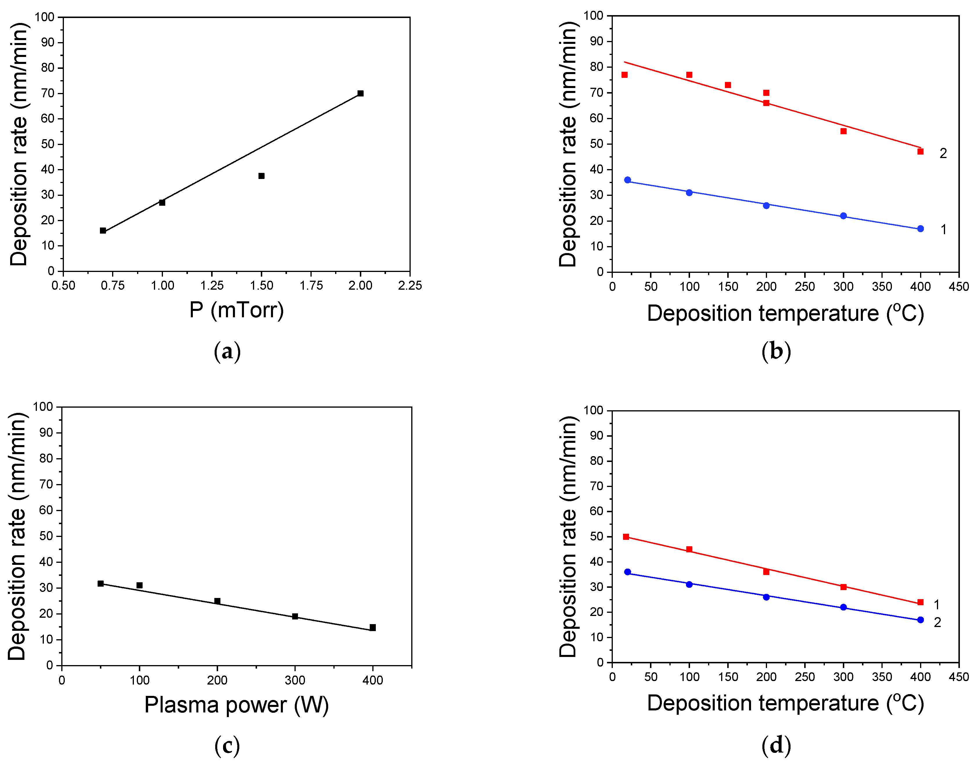
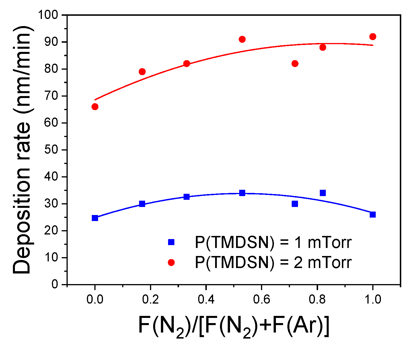
3.1. Film Growth Rate
3.2. Structure and Morphology Study
3.2.1. XRD Characterization
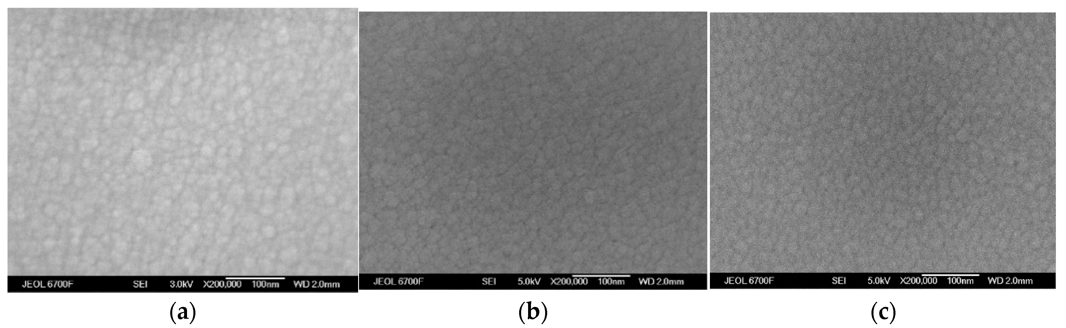
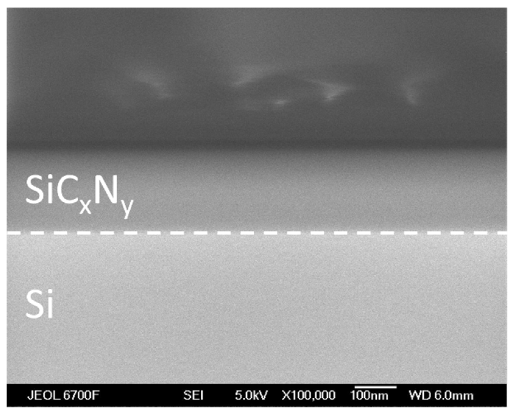
3.2.2. Surface Morphology Study
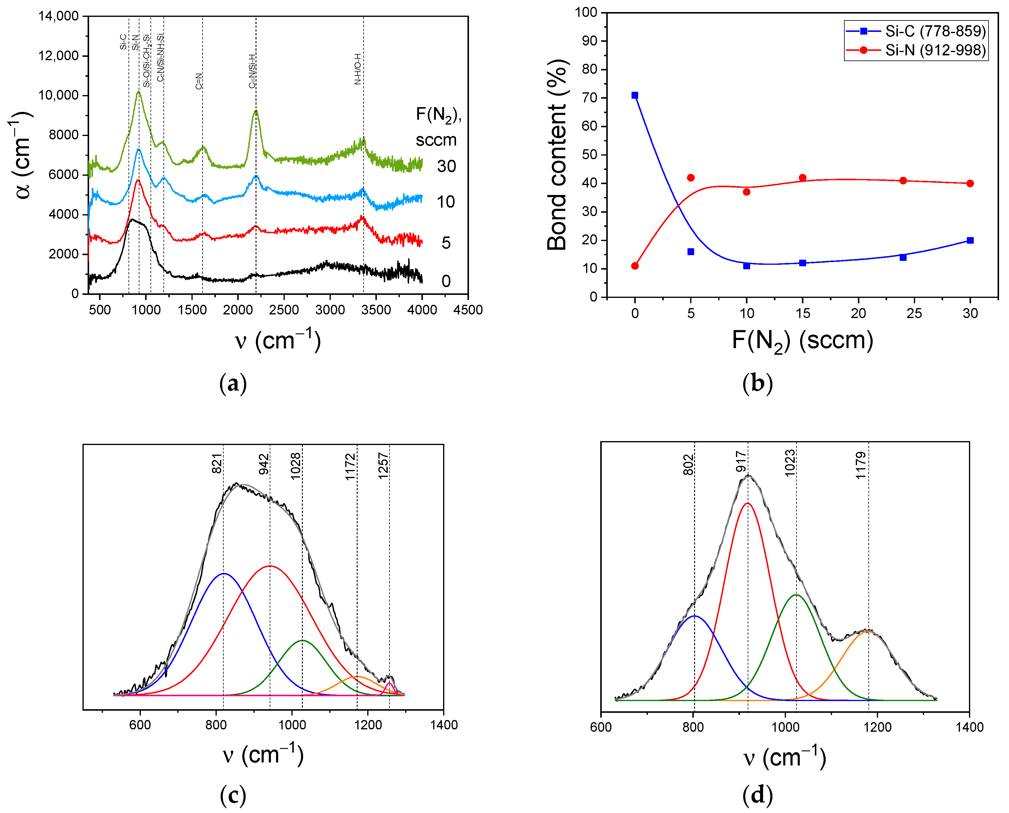
3.3. Chemical Composition of SiCxNy:H Films
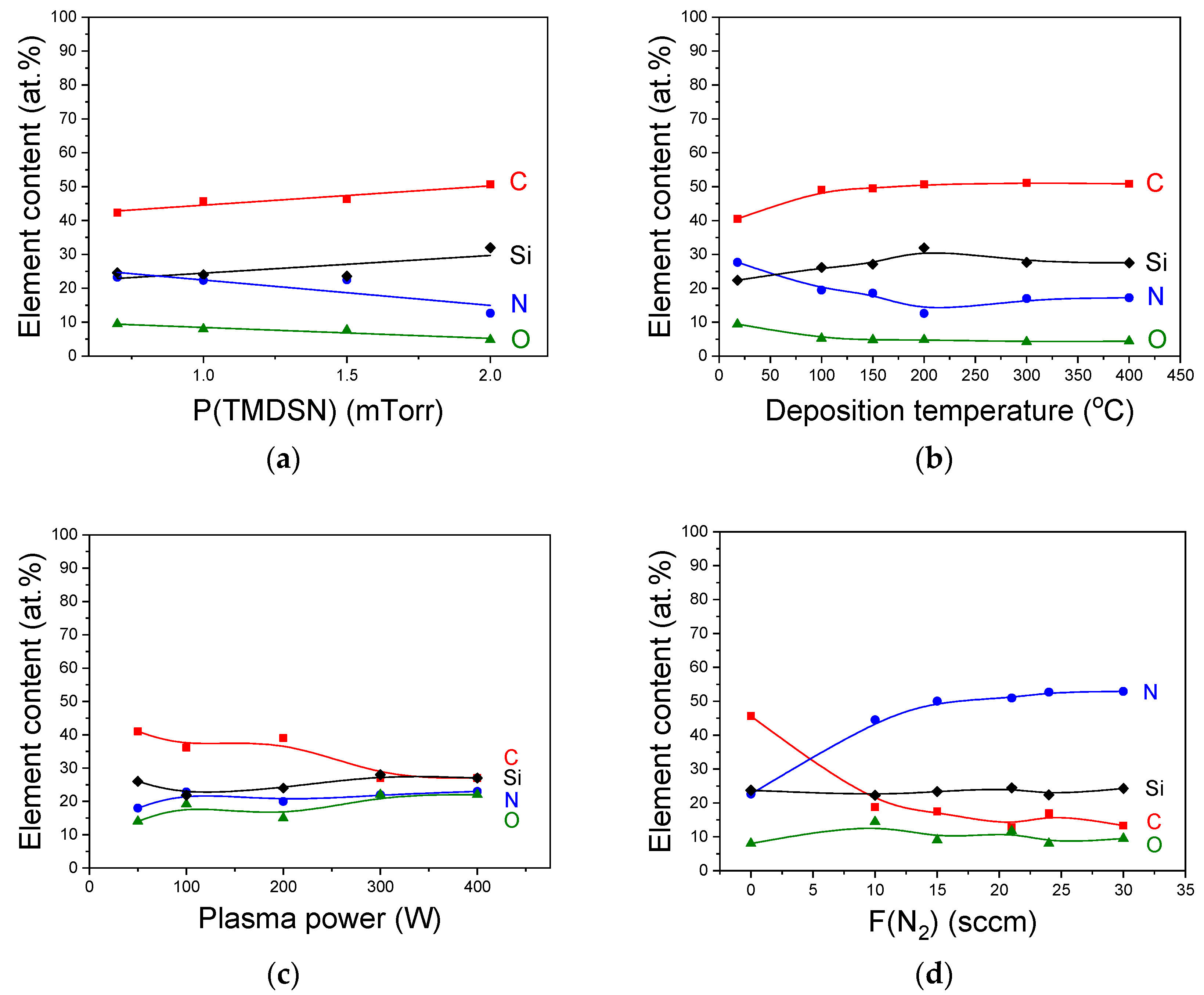
3.3.1. EDX Data
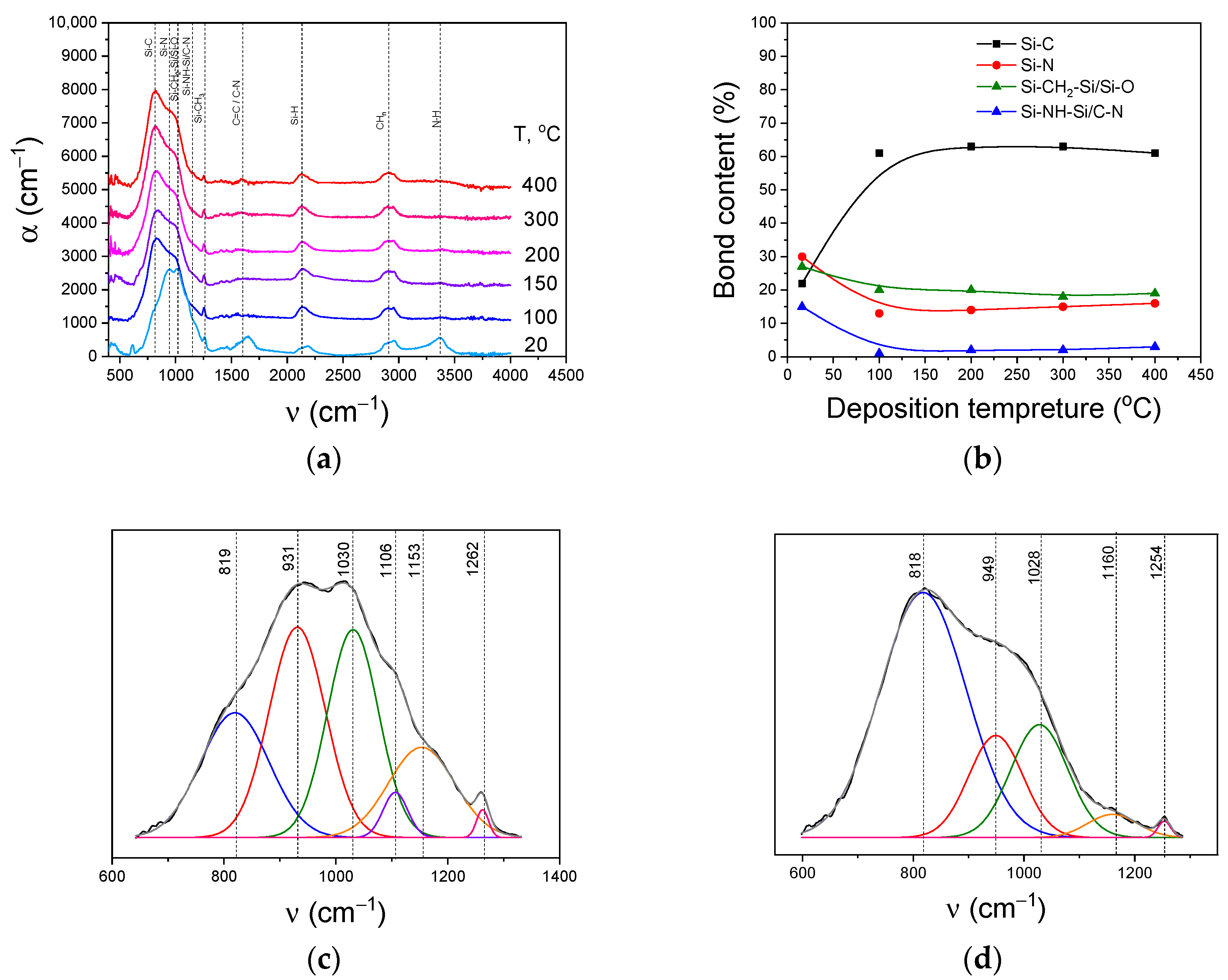
3.3.2. Film Chemical Bonding State
3.3.3. Raman Spectroscopy
3.3.4. Chemical Composition by XPS
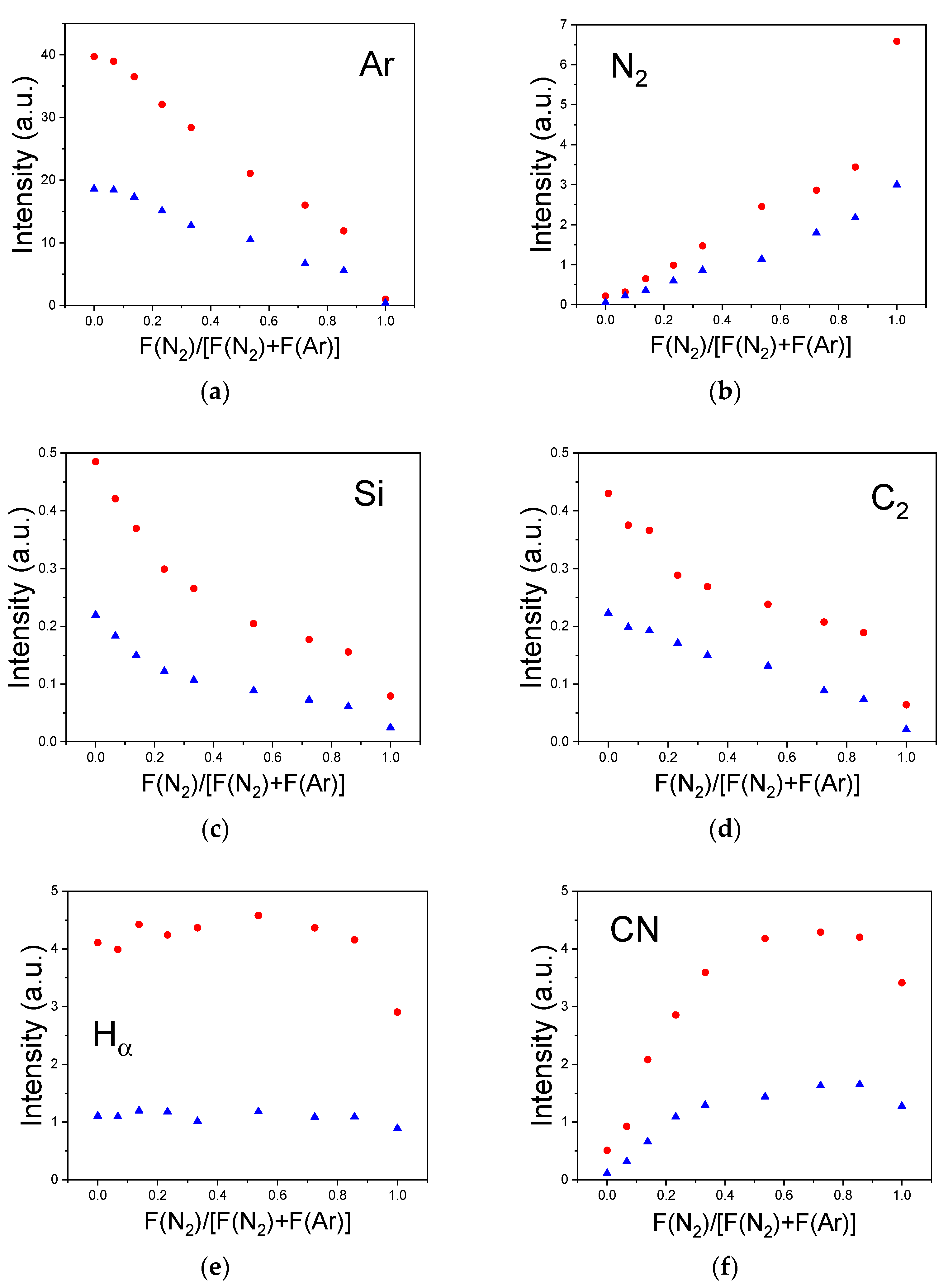
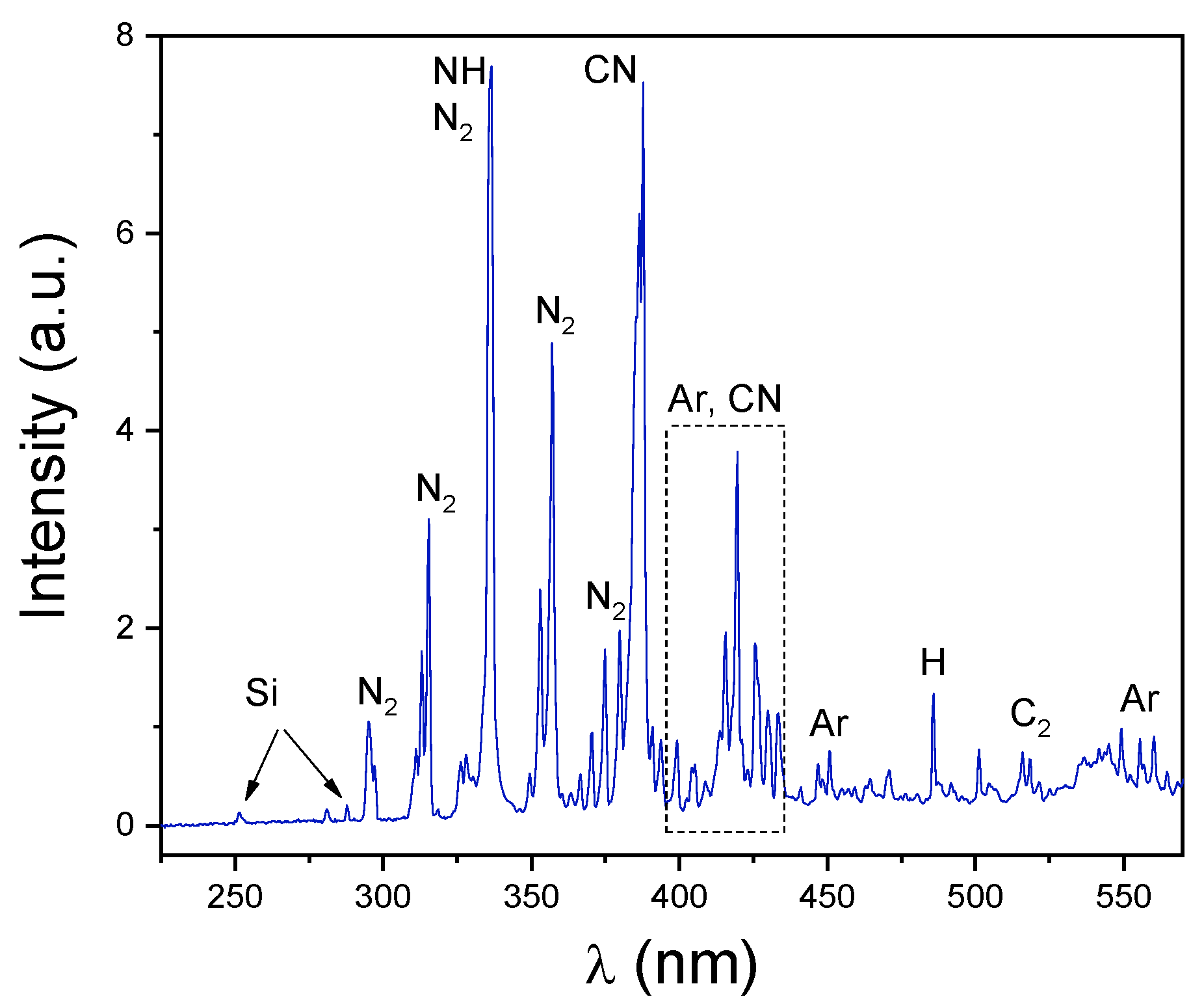
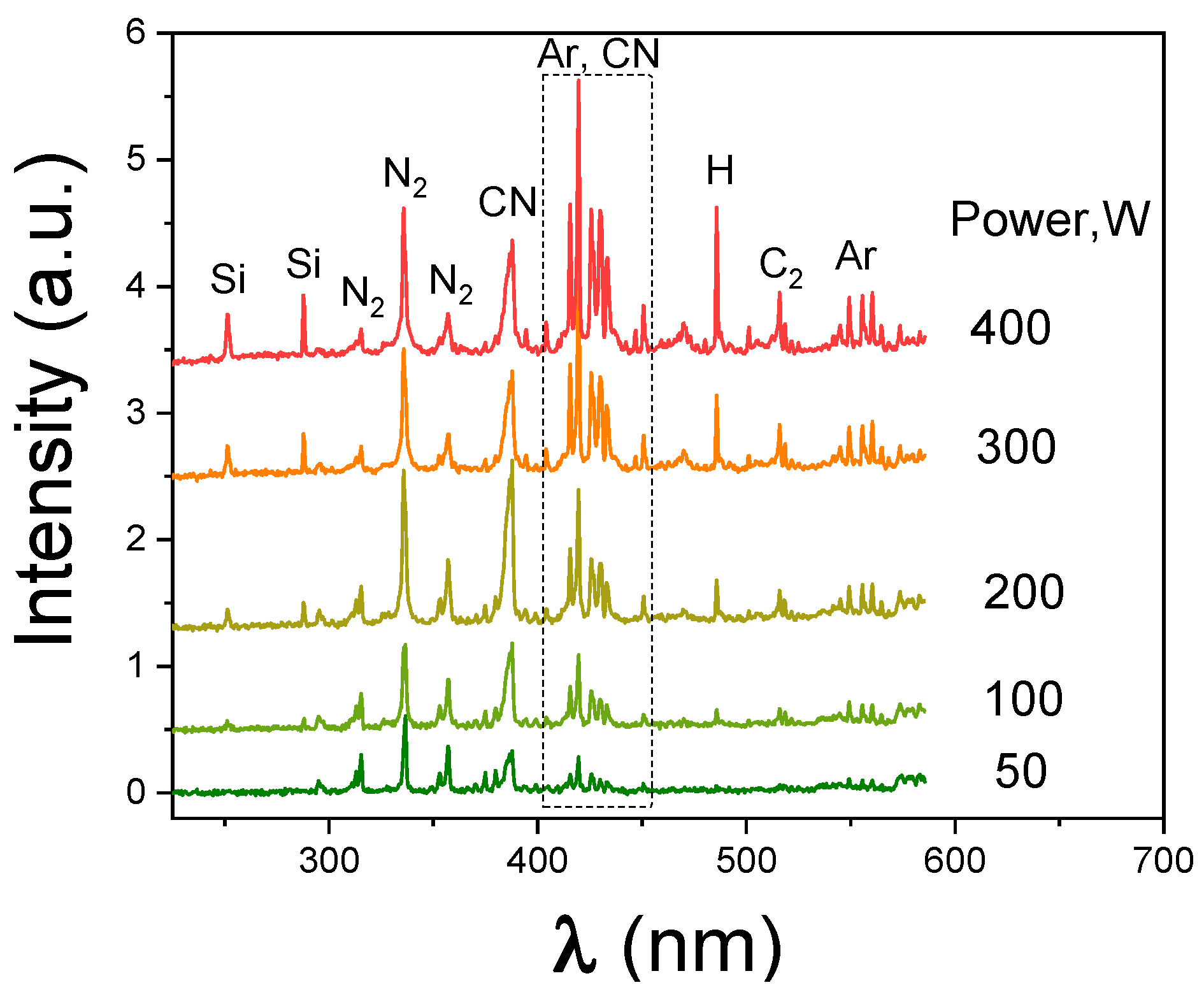
3.4. Gas Phase Composition
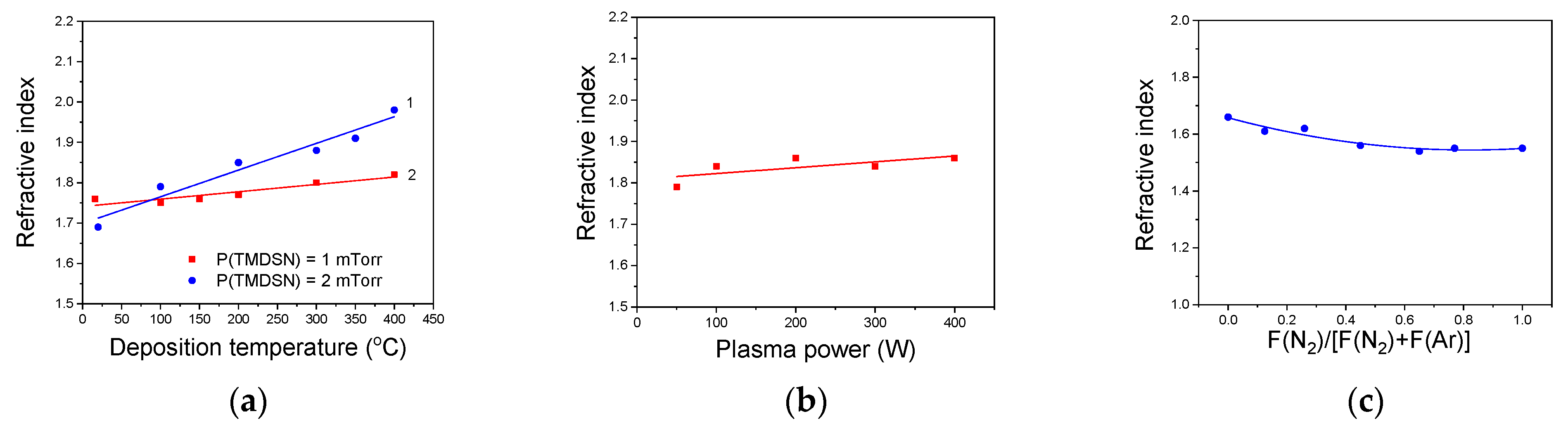
3.5. Functional Characteristics of a-SiCxNy:H Films
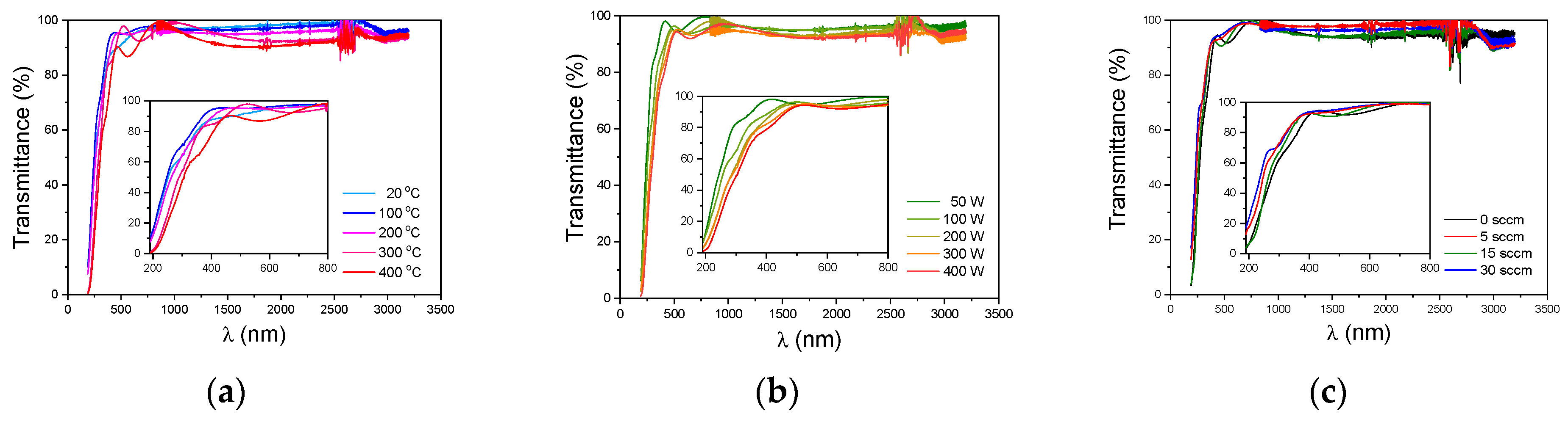
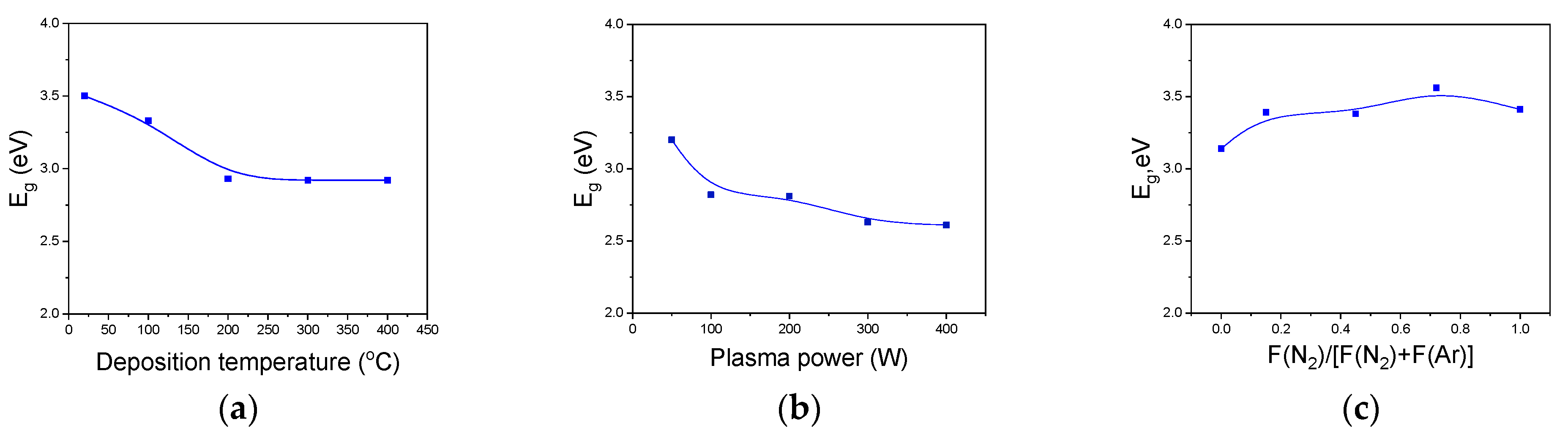
3.5.1. Optical Properties of a-SiCxNy:H Films
3.5.2. Mechanical Properties of Films
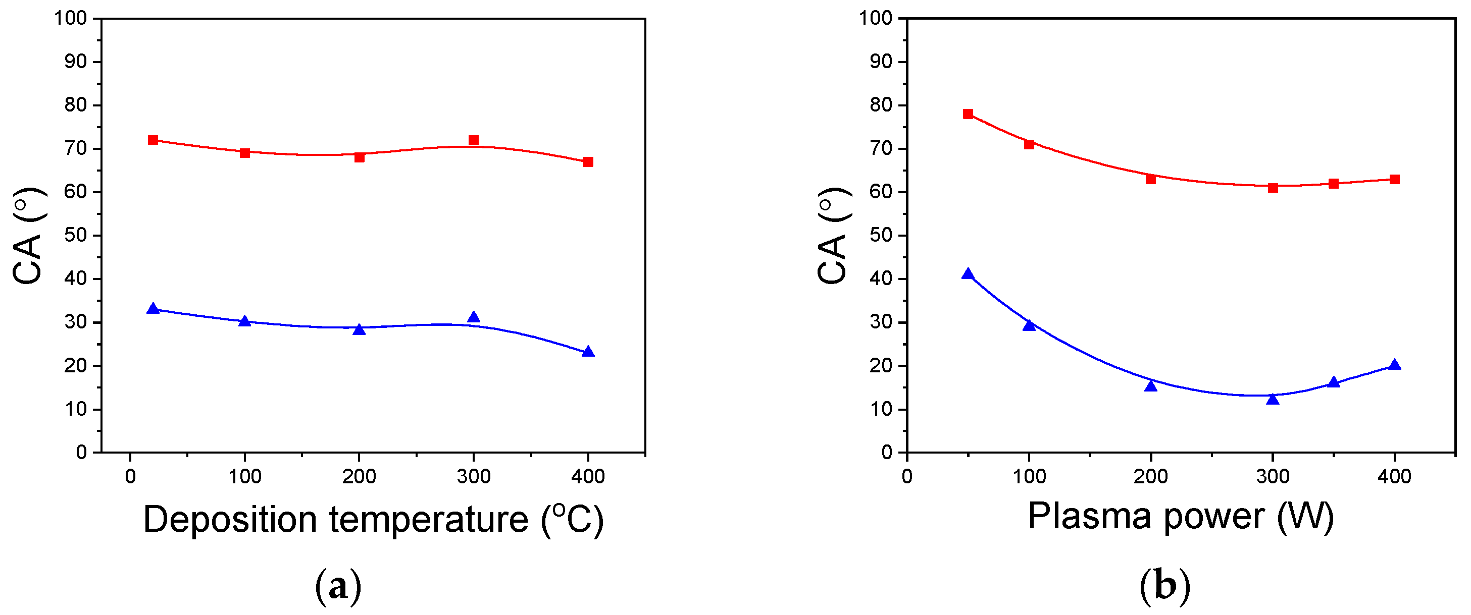
3.5.3. Wettability of a-SiCxNy:H Films
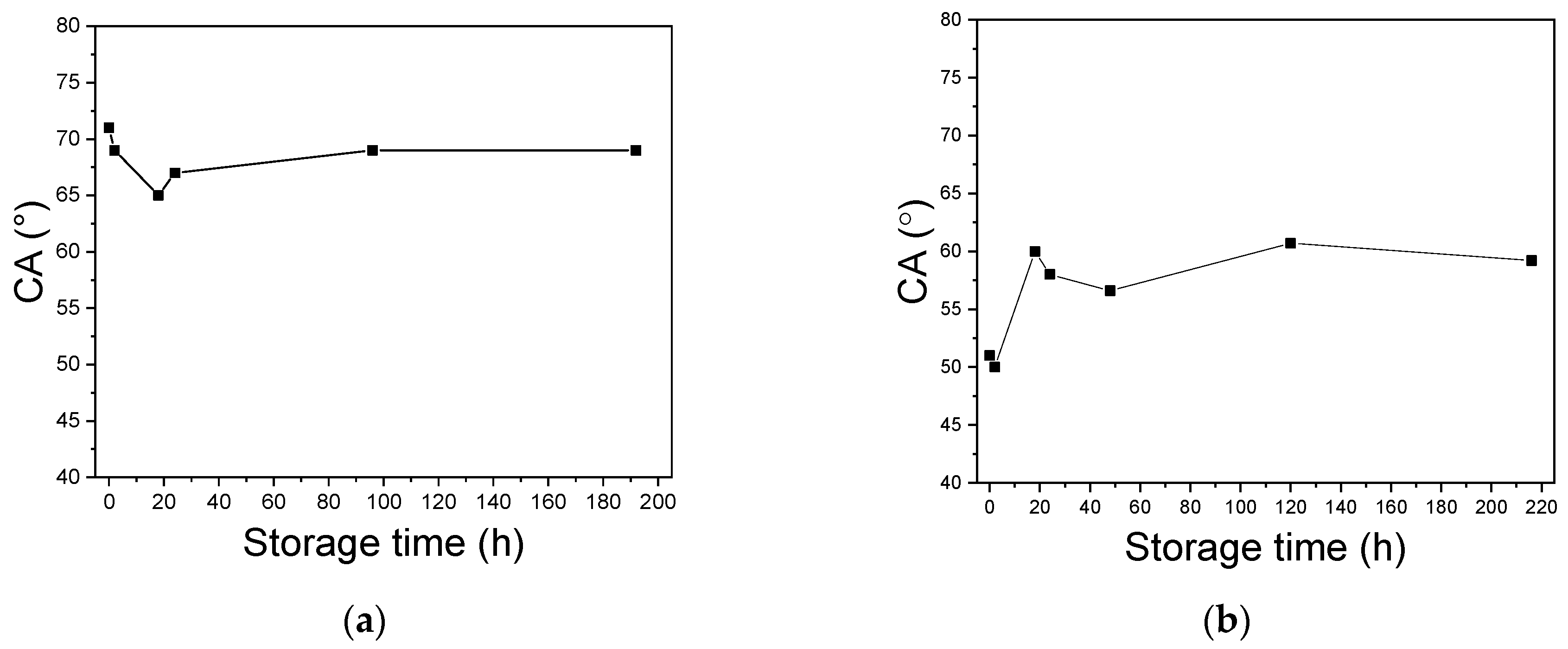
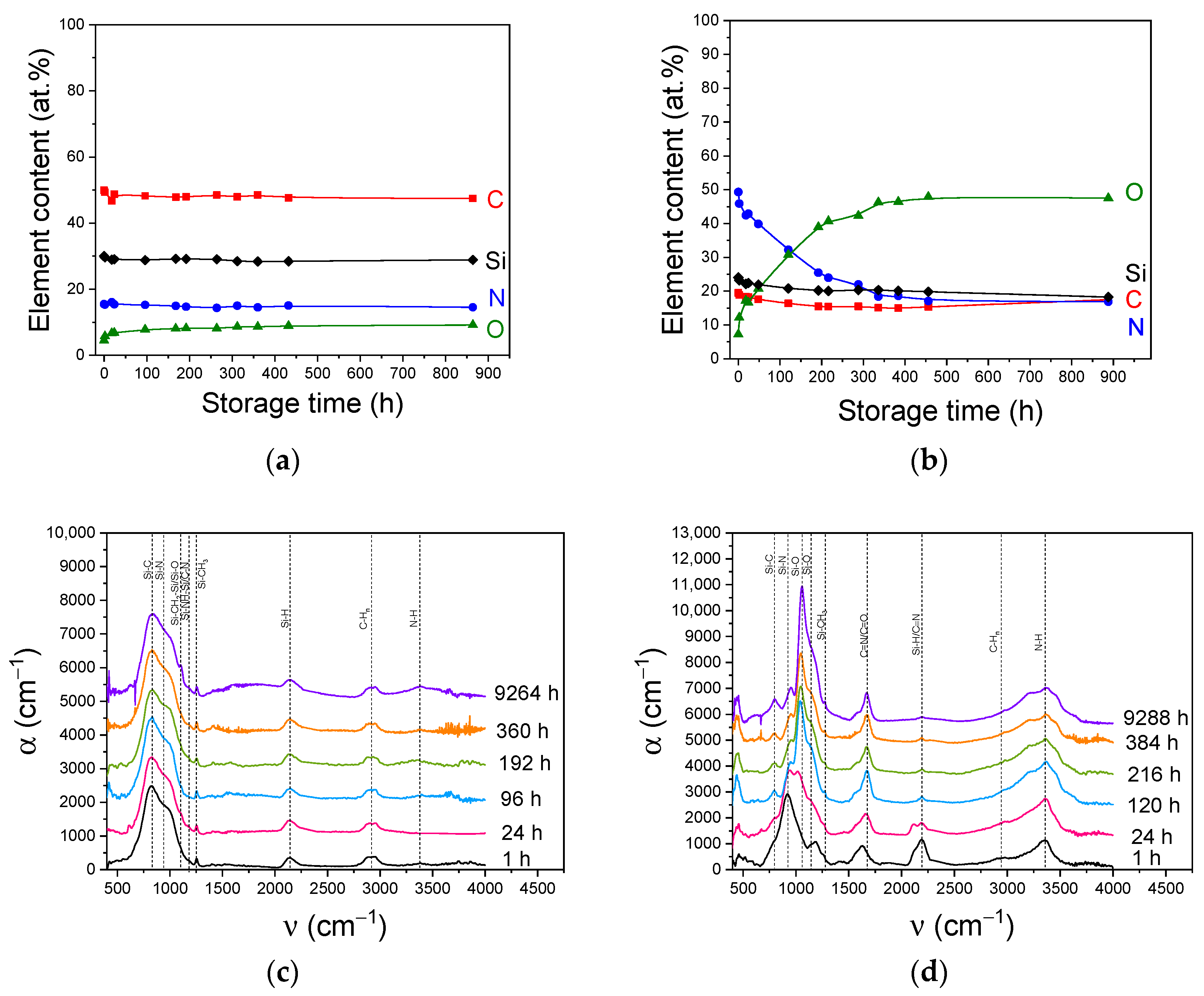
3.6. Aging Behavior of a-SiCxNy:H Films
4. Conclusions
Supplementary Materials
Author Contributions
Funding
Institutional Review Board Statement
Informed Consent Statement
Data Availability Statement
Acknowledgments
Conflicts of Interest
References
- Ermakova, E.; Kosinova, M. Organosilicon compounds as single-source precursors for SiCN films production. J. Organomet. Chem. 2022, 958, 122183. [Google Scholar] [CrossRef]
- Hoffmann, P.; Fainer, N.; Kosinova, M.; Baake, O.; Ensinger, W. Chapter 21. Compilation on Synthesis, Characterization and Properties of Silicon and Boron Carbonitride Films. In Silicon Carbide—Materials, Processing and Applications in Electronic Devices; Mukherjee, M., Ed.; InTech: Rijeka, Croatia, 2011; pp. 487–546. ISBN 9789533079684. [Google Scholar]
- Fainer, N.I. From Organosilicon Precursors to Multifunctional Silicon Carbonitride. Russ. J. General Chem. 2012, 82, 43–52. [Google Scholar] [CrossRef]
- Li, Q.; Chen, C.; Xu, M.; Wang, Y.; Wang, X.; Zhang, Z.; Zhao, W.; Stiens, J. Blue-violet emission of silicon carbonitride thin films prepared by sputtering and annealing treatment. Appl. Surf. Sci. 2021, 546, 149121. [Google Scholar] [CrossRef]
- Zhang, S.; Li, Y.; Yang, H.; Meng, Q.; Wang, W.; Li, H.; Huang, C.; Nishimura, A.; Li, J.; Li, L. Multifunctional Superhydrophobic Composite Coatings with Remarkable Passive Heat Dissipation and Anticorrosion Properties. Ind. Eng. Chem. Res. 2021, 60, 11019–11029. [Google Scholar] [CrossRef]
- Sundaram, K.; Alizadeh, Z.; Todi, R.; Desai, V. Investigations on hardness of RF sputter deposited SiCN thin films. Mater. Sci. Eng. 2004, 368, 103–108. [Google Scholar] [CrossRef]
- Wrobel, A.M.; Kryszewski, M.; Gazicki, M. Mechanism of polysilazane thin film formation during glow discharge polymerization of hexamethylcyclotrisilazane. Polymer 1976, 17, 673–677. [Google Scholar] [CrossRef]
- Gazicki, M.; Wrobel, A.M.; Kruszewski, M. Studies on soluble fraction of glow-discharge polysilazane formed from hexamethylcyclotrisilazane. J. Appl. Polym. Sci. 1977, 21, 2013–2019. [Google Scholar] [CrossRef]
- Wróbel, A.M.; Kryszewski, M. Effect of glow discharge conditions on structure and thermal properties of polysilazane thin films. J. Macromol. Sci. Chem. A 1978, 12, 1041–1054. [Google Scholar] [CrossRef]
- Hirotsu, T. Some surface properties of plasma polymers prepared from hexamethyldisilazane and diethylaminotrimethylsilane. Appl. Polym. 1979, 24, 1957–1964. [Google Scholar] [CrossRef]
- Voronkov, M.G.; Sulimin, A.D.; Yachmenev, V.V.; Mirskov, R.G.; Kokin, V.N.; Chernova, V.G. Production of silicon-nitride films from hexamethylcyclotrisilazane in a high-frequency glow-discharge. Dokl. Akad. Nauk SSSR 1981, 259, 1130–1132. [Google Scholar]
- Bielinski, D.; Wrobel, A.M.; Walkiewicz-Pietrzykowskab, A. Mechanical and tribological properties of thin remote microwave plasma CVD a-Si:N:C films from a single-source precursor. Tribol. Lett. 2002, 13, 71–76. [Google Scholar] [CrossRef]
- Wróbel, A.M.; Błaszczyk, I.; Walkiewicz-Pietrzykowska, A.; Tracz, A.; Klemberg-Sapieha, J.E.; Aoki, T.; Hatanaka, Y. Remote hydrogen–nitrogen plasma chemical vapor deposition from a tetramethyldisilazane source. Part 1. Mechanism of the process, structure and surface morphology of deposited amorphous hydrogenated silicon carbonitride films. J. Mater. Sci. 2003, 13, 731–737. [Google Scholar]
- Wróbel, A.M.; Błaszczyk, I.; Walkiewicz-Pietrzykowska, A.; Bieliński, D.M.; Aoki, T.; Hatanaka, Y. Silicon Carbonitride Films by Remote Hydrogen-Nitrogen Plasma CVD from a Tetramethyldisilazane Source. J. Electrochem. Soc. 2004, 151, C723–C730. [Google Scholar] [CrossRef]
- Blaszczyk-Lezak, I.; Wrobel, A.M.; Aoki, T.; Nakanishi, Y.; Kucinska, I.; Tracz, A. Remote nitrogen microwave plasma chemical vapor deposition from a tetramethyldisilazane precursor. 1. Growth mechanism, structure, and surface morphology of silicon carbonitride films. Thin Solid Films 2006, 497, 24–34. [Google Scholar] [CrossRef]
- Blaszczyk-Lezak, I.; Wrobel, A.; Bielinski, D. Remote nitrogen microwave plasma chemical vapor deposition from a tetramethyldisilazane precursor. 2. Properties of deposited silicon carbonitride films. Thin Solid Films 2006, 497, 35–41. [Google Scholar] [CrossRef]
- Wrobel, A.M.; Blaszczyk-Lezak, I.; Walkiewicz-Pietrzykowska, A. Silicon Carbonitride thin-film coatings fabricated by remote hydrogen–nitrogen microwave plasma chemical vapor deposition from a single-source precursor: Growth process, structure, and properties of the coatings. J. Appl. Polym. Sci. 2007, 105, 122–129. [Google Scholar] [CrossRef]
- Wrobel, A.M.; Blaszczyk-Lezak, I. Remote hydrogen microwave plasma CVD of silicon carbonitride films from a tetramethyldisilazane source. Part 1: Characterization of the process and structure of the films. Chem. Vap. Depos. 2007, 13, 595–600. [Google Scholar] [CrossRef]
- Wrobel, A.M.; Blaszczyk-Lezak, I. Remote Hydrogen Microwave Plasma CVD of Silicon Carbonitride Films From a Tetramethyldisilazane Source. Part 2: Compositional and Structural Dependencies of Film Properties. Chem. Vap. Depos. 2007, 13, 601–608. [Google Scholar] [CrossRef]
- Wrobel, A.M.; Uznanski, P. Hard silicon carbonitride thin-film coatings produced by remote hydrogen plasma chemical vapor deposition using aminosilane and silazane precursors. 1: Deposition mechanism, chemical structure, and surface morphology. Plasma Processes Polym. 2021, 18, e2000240. [Google Scholar] [CrossRef]
- Wrobel, A.M.; Uznanski, P. Hard silicon carbonitride thin-film coatings by remote hydrogen plasma chemical vapor deposition using aminosilane and silazane precursors. 2: Physical, optical, and mechanical properties of deposited films. Plasma Processes Polym. 2021, 18, e2000241. [Google Scholar] [CrossRef]
- Guruvenket, S.; Andrie, S.; Simon, M.; Johnson, K.W.; Sailer, R.A. Atmospheric-Pressure Plasma-Enhanced Chemical Vapor Deposition of a-SiCN:H Films: Role of Precursors on the Film Growth and Properties. ACS Appl. Mater. Interfaces 2012, 4, 5293–5299. [Google Scholar] [CrossRef]
- Fainer, N.I.; Golubenko, A.N.; Rumyantsev, Y.u.M.; Kesler, V.G.; Maximovskii, E.A.; Ayupov, B.M.; Kuznetsov, F.A. Synthesis of Silicon Carbonitride Dielectric Films with Improved Optical and Mechanical Properties from Tetramethyldisilazane. Glass Phys. Chem. 2013, 39, 77–88. [Google Scholar] [CrossRef]
- Sobczyk-Guzenda, A.; Oleśko, K.; Gazicki-Lipman, M.; Szymański, W.; Balcerzak, J.; Wendler, B.; Szymanowski, H. Chemical structure and optical properties of a-SiNC coatings synthesized from different disilazane precursors with the RF plasma enhanced CVD technique—A comparative study. Mater. Res. Express 2019, 6, 016410. [Google Scholar] [CrossRef]
- Szymanowski, H.; Olesko, K.; Kowalski, J.; Fijalkowski, M.; Gazicki-Lipman, M.; Sobczyk-Guzenda, A. Thin SiNC/SiOC coatings with a gradient of refractive index deposited from organosilicon precursor. Coatings 2020, 10, 794. [Google Scholar] [CrossRef]
- Belmahi, M.; Bulou, S.; Thouvenin, A.; de Poucques, L.; Hugon, R.; Le Brizoual, L.; Miska, P.; Geneve, D.; Vasseur, J.-L.; Bougdira, J. Microwave Plasma Process for SiCN:H Thin Films Synthesis with Composition Varying from SiC:H to SiN:H in H2/N2/Ar/Hexamethyldisilazane Gas Mixture. Plasma Processes Polym. 2014, 11, 551–558. [Google Scholar] [CrossRef]
- Jiang, L.; Tian, H.; Li, J.; Xiang, P.; Peng, Y.; Wang, T.; Hou, P.; Xiao, T.; Tan, X. The influence of NH3 flow rate on the microstructure and oxidation properties of a-Si-C-N:H films prepared by PECVD technology. Appl. Surf. Sci. 2020, 513, 145861. [Google Scholar] [CrossRef]
- Huber, C.; Stein, B.; Kalt, H. Plasma-enhanced chemical vapor deposition of amorphous silicon carbonitride: Deposition temperature dependence of bonding structure, refractive index, mechanical stress and their aging under ambient air. Thin Solid Films 2017, 634, 66–72. [Google Scholar] [CrossRef]
- Gengenbach, T.R.; Griesser, H. Post-deposition ageing reactions differ markedly between plasma polymers deposited from siloxane and silazane monomers. Polymer 1999, 40, 5079–5094. [Google Scholar] [CrossRef]
- Sukhanov, Y.N.; Ershov, A.P.; Rudenko, K.V.; Orlikovsky, A.A. Comparative study of inductively coupled and microwave BF3 plasmas for microelectronic technology applications. In Proceedings of the Micro- and Nanoelectronics 2003, Zvenigo-rod, Russia, 28 May 2004; pp. 55–64. [Google Scholar]
- Zhang, Y.; Tang, J.; Hu, Y.; Yuan, J.; Guan, L.; Li, X.; Cui, X.; Ding, G.; Shi, X.; Xu, K.; et al. Effect of hydrogen content on dielectric strength of the silicon nitride film deposited by ICP-CVD. Chin. Phys. B 2021, 30, 048103. [Google Scholar] [CrossRef]
- Wu, H.-Y.; Hsu, C.-H.; Liu, T.-X.; Ou, Y.-C.; Hsu, Y.-H.; Wu, W.-Y.; Lien, S.-Y.; Jiang, Y.-L. Silicon nitride cover layer prepared by silane-free plasma chemical vapor deposition for high quality surface passivation of silicon solar cells. Surf. Coat. Technol. 2019, 376, 68–73. [Google Scholar] [CrossRef]
- Bang, S.-H.; Suk, J.-H.; Kim, K.-S.; Park, J.-H.; Hwang, N.-M. Effects of radio frequency power and gas ratio on barrier properties of SiOxNy films deposited by inductively coupled plasma chemical vapor deposition. Thin Solid Films 2019, 669, 108–113. [Google Scholar] [CrossRef]
- Qiu, P.; Wu, B.; Fu, P.; Li, M.; Xie, Y.; Kan, Q. Fabrication and Characterization of Low-Threshold Single Fundamental Mode VCSELs With Dielectric DBR Mirror. IEEE Photonics J. 2021, 13, 1500106. [Google Scholar] [CrossRef]
- Mundo, R.D.; d’Agostino, R.; Fracassi, F.; Palumbo, F. A Novel organosilicon source for low temperature plasma deposition of silicon nitride-like thin films. Plasma Processes Polym. 2005, 2, 612–617. [Google Scholar] [CrossRef]
- Fainer, N.I.; Kosinova, M.L.; Maximovsky, E.A.; Rumyantsev, Y.M.; Kuznetsov, F.A.; Kesler, V.G.; Kirienko, V.V. Study of the structure and phase composition of nanocrystalline silicon oxynitride films synthesized by ICP-CVD. Nucl. Instr. Meth. Phys. Res. 2005, 543, 134–138. [Google Scholar] [CrossRef]
- Rumyantsev, Y.M.; Chagin, M.N.; Kosinova, M.L.; Kuznetsov, F.A. Synthesis of thin silicon carbonitride films from hexamethyldisilazane in an inductively coupled plasma reactor. Inorg. Mater. 2015, 51, 897–902. [Google Scholar] [CrossRef]
- Shayapov, V.R.; Chagin, M.N.; Kolodin, A.N.; Kosinova, M.L. Deposition of Films from a Mixture of Hexamethylcyclotrisilazane Vapor and Argon in Inductively Coupled Plasma. Glass Phys. Chem. 2019, 45, 525–531. [Google Scholar] [CrossRef]
- Rumyantsev, Y.M.; Chagin, M.N.; Shayapov, V.R.; Yushina, I.V.; Kichai, V.N.; Kosinova, M.L. Synthesis and Properties of Thin Films Formed by Vapor Deposition from Tetramethylsilane in a Radio-Frequency Inductively Coupled Plasma Discharge. Glass Phys. Chem. 2018, 44, 174–182. [Google Scholar] [CrossRef]
- Orlikovsky, A.A.; Rudenko, K.V.; Averkin, S.N. Fine-Line Plasma-Enhanced Processes on the Basis of a Set of Pilot Units with a Scalable Inductively Coupled Plasma Source for Use in Microelectronics. High Energy Chem. 2006, 40, 182–193. [Google Scholar] [CrossRef]
- Scofield, J.H. Hartree-Slater subshell photoionization cross-sections at 1254 and 1487 eV. J. Electron Spectrosc. Relat. Phenom. 1976, 8, 129–137. [Google Scholar] [CrossRef]
- Shirley, D.A. High-Resolution X-Ray Photoemission Spectrum of the Valence Bands of Gold. Phys. Rev. B 1972, 5, 4709–4714. [Google Scholar] [CrossRef] [Green Version]
- CasaXPS: Processing Software for XPS, AES, SIMS and More. Available online: www.casaxps.com (accessed on 30 December 2021).
- Pearse, R.W.B.; Gaydon, A.G. The Identification of Molecular Spectra; John Wiley and Sons: Hoboken, NY, USA, 1963. [Google Scholar]
- Dieke, G.H. The Hydrogen Molecule Wavelength Tables of Gerhard Heinrich Dieke; Crosswhite, H.M., Ed.; Wiley-InterScience: New York, NY, USA, 1972; ISBN 0471188905. [Google Scholar]
- NIST Atomic Spectra Database; NIST Standard Reference Database 78 Version 5.9. Available online: https://physics.nist.gov/asd (accessed on 10 December 2021).
- Kwok, D.Y.; Neumann, A.W. Contact angle measurements and contact angle interpretation. Adv. Colloid Interface Sci. 1999, 81, 167–249. [Google Scholar] [CrossRef]
- Owens, D.K.; Wendt, R.C. Estimation of the surface free energy of polymers. J. Appl. Polym. Sci. 1969, 13, 1741–1747. [Google Scholar] [CrossRef]
- Wu, S. Polymer Interface and Adhesion; Marcel Dekker: New York, NY, USA, 1982; ISBN 9780824715335. [Google Scholar]
- Vassallo, E.; Cremona, A.; Ghezzi, F.; Dellera, F.; Laguardia, L.; Ambrosone, G.; Coscia, U. Structural and optical properties of amorphous hydrogenated silicon carbonitride films produced by PECVD. Appl. Surf. Sci. 2006, 252, 7993–8000. [Google Scholar] [CrossRef]
- Bellamy, L.J. The Infrared Spectra of Complex Molecules; Springer: London, UK, 1980; ISBN 9780412223501. [Google Scholar]
- Anderson, D.R. Chap. 10. Infrared, Raman, and Ultraviolet Spectroscopy. In Analysis of Silicones; Smith, A.L., Ed.; Wiley-Interscience: New York, NY, USA, 1974. [Google Scholar]
- Rao, C.N.R. Chemical Applications of Infrared Spectroscopy; Academic Press: New York, NY, USA, 1963. [Google Scholar]
- Launer, P.J.; Arkles, B. Infrared analysis of organosilicon compounds: Spectra-structure correlations. In Silicon Compounds: Silanes & Silicones; Gelest, Inc.: Morrisville, PA, USA, 2013; pp. 175–178. [Google Scholar]
- Tolstoy, V.P.; Chernyshova, I.V.; Skryshevsky, V.A. Handbook of Infrared Spectroscopy of Ultrathin Films; Wiley-Interscience: Hoboken, NY, USA, 2003; ISBN 047135404X. [Google Scholar]
- Ferrari, A.C.; Robertson, J. Interpretation of Raman spectra of disordered and amorphous carbon. Phys. Rev. B 2000, 61, 14095–14107. [Google Scholar] [CrossRef] [Green Version]
- Jamroz, P.; Zyrnicki, W. Spectroscopic study of the decomposition process of tetramethylsilane in the N2–H2 and N2–Ar low pressure plasma. Diam. Relat. Mater. 2005, 14, 1498–1507. [Google Scholar] [CrossRef]
- Tauc, J.; Menth, A. States in the gap. J. Non-Cryst. Solids 1972, 8, 569–585. [Google Scholar] [CrossRef]
- Wrobel, A.M. Aging process in plasma-polymerized organosilicon thin films. J. Macromol. Sci.-Chem. 1985, 22, 1089–1100. [Google Scholar] [CrossRef]


| Series | Addition Gas | R(N2) = F(N2)/[F(N2) + F(Ar)] | TMDSN Pressure, mTorr | Substrate Temperature, °C | Plasma Power, W |
|---|---|---|---|---|---|
| A | Ar | - | 0.7–2 | 200 | 200 |
| B | Ar | - | 1 | 20–400 | 200 |
| C | Ar | - | 2 | 20–400 | 200 |
| D | Ar | - | 1 | 200 | 50–400 |
| E | Ar | - | 1 | 20–400 | 100 |
| F | Ar + N2 | 0–1 | 1 | 300 | 200 |
| G | Ar + N2 | 0–1 | 2 | 200 | 200 |
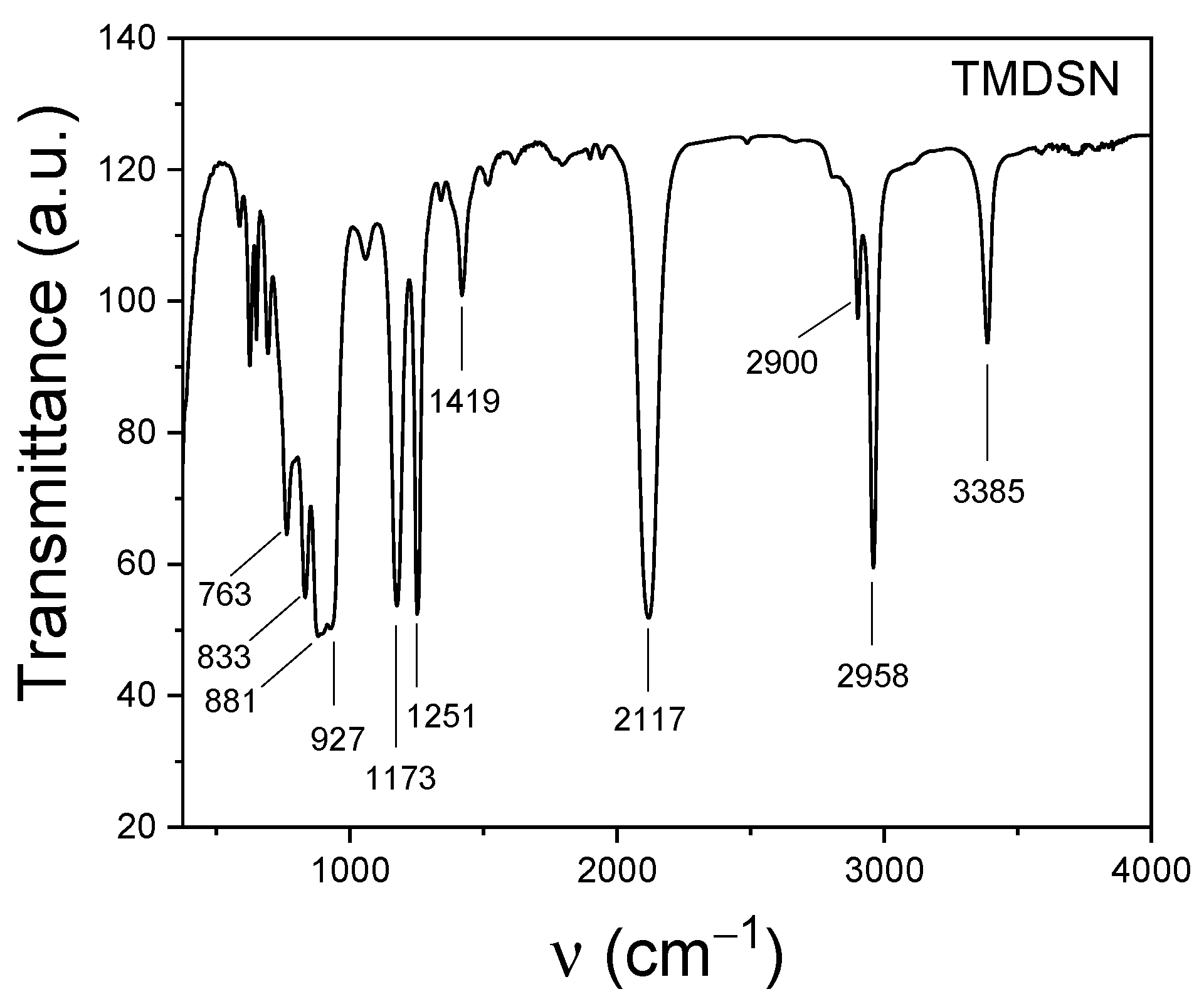
| TMDSN | ||
|---|---|---|
| Peak Position (cm−1) | Assignment | Structural Fragment |
| 3385 | ν(NH) | Si–NH–Si |
| 2958 | νa(CH) | CH3 |
| 2900 | νs(CH) | CH3 |
| 2117 | ν(SiH) | SiH |
| 1518 | δ(NH) | Si–NH–Si |
| 1419 | δa(CH) | CH3 |
| 1250 | δs(CH) | Si–CH3 |
| 1173 | δ(NH) | Si–NH–Si |
| 927 | νs(Si-N-Si) | Si–NH–Si |
| 881 | δ(CH) | Si(CH3)2 |
| 833 | ρ(CH) | Si(CH3)2 |
| 763 | ν(SiC) | –Si–C– |
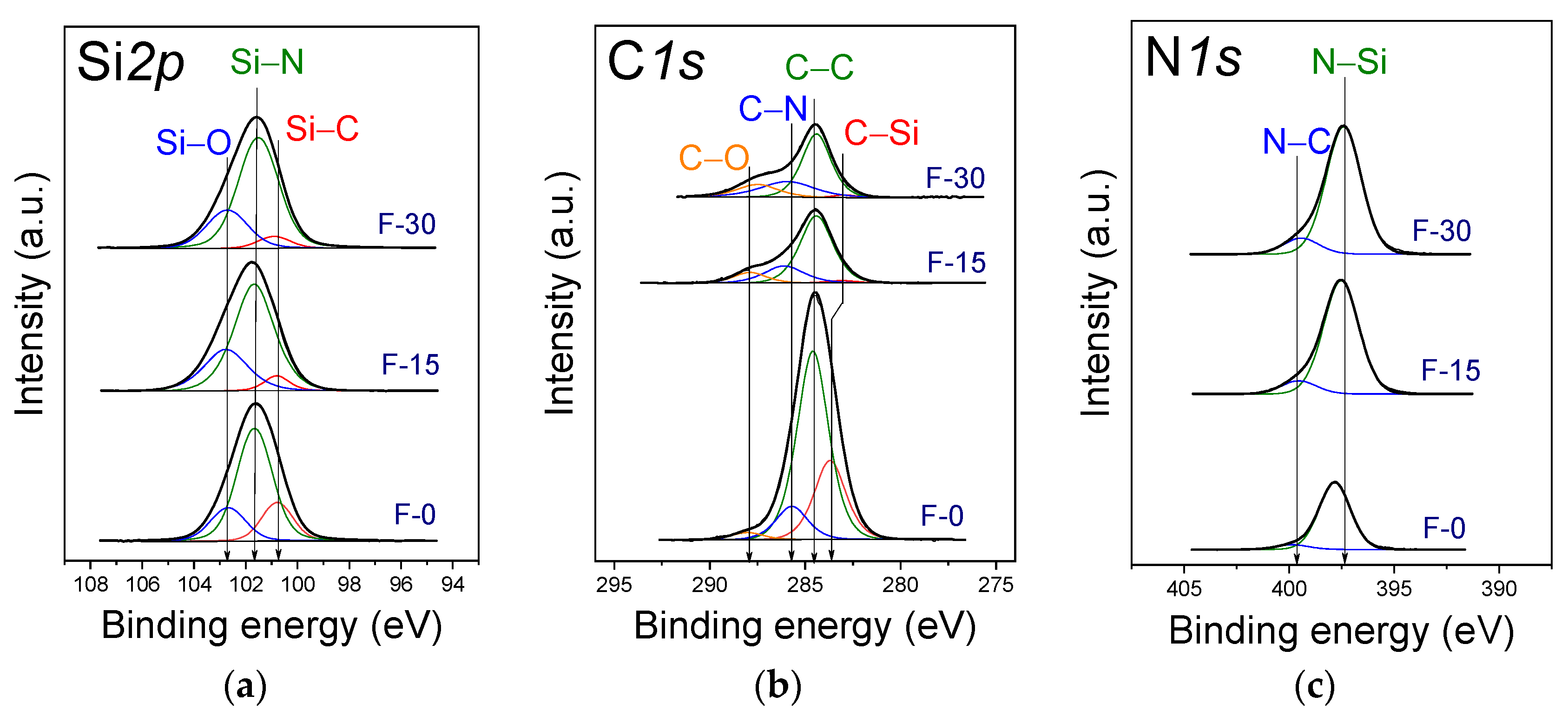
| Samples | F(N2), sccm | Element Composition | |||
|---|---|---|---|---|---|
| Si, at.% | C, at.% | N, at.% | O, at.% | ||
| F-0 | 0 | 27 (26) | 43 (38) | 14 (24) | 16 (10) |
| F-15 | 15 | 29 (27) | 15 (12) | 28 (49) | 28 (11) |
| F-30 | 30 | 29 (27) | 15 (10) | 32 (55) | 24 (6) |
| Sample | Eb, eV (Content, %) | ||||||||
|---|---|---|---|---|---|---|---|---|---|
| Si2p | C1s | N1s | |||||||
| Si–O | Si–N | Si–C | C–O | C–N | C–C | C–Si | N–C | N–Si | |
| F-0 | 102.7 (18%) | 101.7 (63%) | 100.8 (19%) | 288.0 (2%) | 285.7 (11%) | 284.6 (61%) | 283.7 (26%) | 399.8 (12%) | 397.3 (88%) |
| F-15 | 102.8 (28%) | 101.7 (66%) | 100.8 (6%) | 287.9 (11%) | 286.1 (21%) | 284.4 (67%) | 283.1 (2%) | 399.5 (14%) | 397.5 (86%) |
| F-30 | 102.7 (25%) | 101.5 (70%) | 100.9 (6%) | 287.5 (16%) | 285.9 (26%) | 284.4 (57%) | 282.9 (2%) | 399.5 (15%) | 397.4 (85%) |
| Deposition Conditions | H, GPa | E, GPa | R, % | ||||
|---|---|---|---|---|---|---|---|
| P(TMDSN), Torr | F(Ar), sccm | F(N2), sccm | Tdep, °C | P, W | |||
| 1 × 10⁻³ | 30 | 0 | 20 | 200 | 3.33 | 57.83 | 41.14 |
| 100 | 3.46 | 52.12 | 41.87 | ||||
| 200 | 4.65 | 61.33 | 47.49 | ||||
| 300 | 9.20 | 78.45 | 62.30 | ||||
| 350 | 12.09 | 99.77 | 70.52 | ||||
| 400 | 13.57 | 106.43 | 66.68 | ||||
| 1 × 10⁻³ | 30 | 0 | 200 | 50 | 5.25 | 50.36 | 47.05 |
| 100 | 3.75 | 38.54 | 47.67 | ||||
| 200 | 4.65 | 61.33 | 47.49 | ||||
| 300 | 5.44 | 61.37 | 46.99 | ||||
| 400 | 10.28 | 89.88 | 53.47 | ||||
| Tdep, °C | Neumann Method | Owens-Wendt Method | Wu Method | ||||
|---|---|---|---|---|---|---|---|
| Es, mN/m | Esd, mN/m | Esp, mN/m | Es, mN/m | Esd, mN/m | Esp, mN/m | Es, mN/m | |
| 20 | 40 ± 3 | 27 ± 3 | 12 ± 2 | 39 ± 4 | 25 ± 2 | 17 ± 2 | 42 ± 4 |
| 100 | 42 ± 2 | 27 ± 2 | 14 ± 1 | 40 ± 3 | 25 ± 2 | 19 ± 2 | 44 ± 4 |
| 200 | 43 ± 3 | 27 ± 3 | 14 ± 2 | 41 ± 4 | 26 ± 3 | 19 ± 3 | 45 ± 4 |
| 300 | 40 ± 2 | 28 ± 2 | 11 ± 1 | 39 ± 2 | 26 ± 2 | 17 ± 2 | 43 ± 3 |
| 400 | 43 ± 3 | 29 ± 2 | 14 ± 1 | 42 ± 3 | 27 ± 2 | 19 ± 2 | 46 ± 3 |
| Plasma Power, W | Neumann Method | Owens-Wendt Method | Wu Method | ||||
|---|---|---|---|---|---|---|---|
| Es, mN/m | Esd, mN/m | Esp, mN/m | Es, mN/m | Esd, mN/m | Esp, mN/m | Es, mN/m | |
| 50 | 37 ± 2 | 26 ± 2 | 10 ± 1 | 35 ± 2 | 23 ± 2 | 15 ± 2 | 38 ± 3 |
| 100 | 41 ± 1 | 28 ± 1 | 11 ± 1 | 40 ± 2 | 26 ± 1 | 17 ± 2 | 43 ± 2 |
| 200 | 46 ± 2 | 29 ± 2 | 16 ± 1 | 45 ± 2 | 28 ± 2 | 21 ± 2 | 49 ± 3 |
| 300 | 47 ± 2 | 28 ± 2 | 18 ± 2 | 46 ± 2 | 28 ± 2 | 22 ± 2 | 50 ± 3 |
| 350 | 46 ± 2 | 28 ± 1 | 17 ± 1 | 45 ± 2 | 28 ± 1 | 22 ± 1 | 49 ± 2 |
| 400 | 46 ± 1 | 27 ± 1 | 17 ± 1 | 44 ± 1 | 27 ± 1 | 21 ± 1 | 48 ± 3 |
| Initial Gas Mixture | Aging | Neumann Method | Owens-Wendt Method | Wu Method | ||||
|---|---|---|---|---|---|---|---|---|
| Es, mN/m | Esd, mN/m | Esp, mN/m | Es, mN/m | Esd, mN/m | Esp, mN/m | Es, mN/m | ||
| TMDSN + Ar | 1 h | 41 ± 1 | 24 ± 1 | 16 ± 1 | 40 ± 2 | 24 ± 1 | 20 ± 1 | 44 ± 2 |
| 120 h | 41 ± 2 | 28 ± 1 | 13 ± 1 | 41 ± 2 | 26 ± 1 | 18 ± 2 | 46 ± 2 | |
| TMDSN + N2 | 1 h | 49 ± 2 | 23 ± 1 | 28 ± 2 | 51 ± 2 | 27 ± 2 | 29 ± 2 | 55 ± 3 |
| 120 h | 45 ± 2 | 26 ± 2 | 19 ± 2 | 45 ± 3 | 27 ± 2 | 23 ± 2 | 49 ± 3 | |
Publisher’s Note: MDPI stays neutral with regard to jurisdictional claims in published maps and institutional affiliations. |
© 2022 by the authors. Licensee MDPI, Basel, Switzerland. This article is an open access article distributed under the terms and conditions of the Creative Commons Attribution (CC BY) license (https://creativecommons.org/licenses/by/4.0/).
Share and Cite
Chagin, M.N.; Sulyaeva, V.S.; Shayapov, V.R.; Kolodin, A.N.; Khomyakov, M.N.; Yushina, I.V.; Kosinova, M.L. Synthesis, Properties and Aging of ICP-CVD SiCxNy:H Films Formed from Tetramethyldisilazane. Coatings 2022, 12, 80. https://doi.org/10.3390/coatings12010080
Chagin MN, Sulyaeva VS, Shayapov VR, Kolodin AN, Khomyakov MN, Yushina IV, Kosinova ML. Synthesis, Properties and Aging of ICP-CVD SiCxNy:H Films Formed from Tetramethyldisilazane. Coatings. 2022; 12(1):80. https://doi.org/10.3390/coatings12010080
Chicago/Turabian StyleChagin, Maksim N., Veronica S. Sulyaeva, Vladimir R. Shayapov, Aleksey N. Kolodin, Maksim N. Khomyakov, Irina V. Yushina, and Marina L. Kosinova. 2022. "Synthesis, Properties and Aging of ICP-CVD SiCxNy:H Films Formed from Tetramethyldisilazane" Coatings 12, no. 1: 80. https://doi.org/10.3390/coatings12010080
APA StyleChagin, M. N., Sulyaeva, V. S., Shayapov, V. R., Kolodin, A. N., Khomyakov, M. N., Yushina, I. V., & Kosinova, M. L. (2022). Synthesis, Properties and Aging of ICP-CVD SiCxNy:H Films Formed from Tetramethyldisilazane. Coatings, 12(1), 80. https://doi.org/10.3390/coatings12010080