
The Effect of RF Sputtering Temperature Conditions on the Structural and Physical Properties of Grown SbGaN Thin Film


Abstract
:
1. Introduction
2. Experimental Details
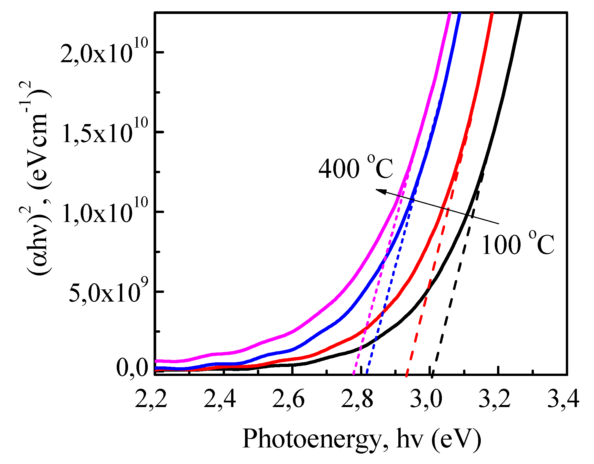
3. Results and Discussion
3.1. Effects of Growth Temperature on the Deposited SbGaN Film Properties
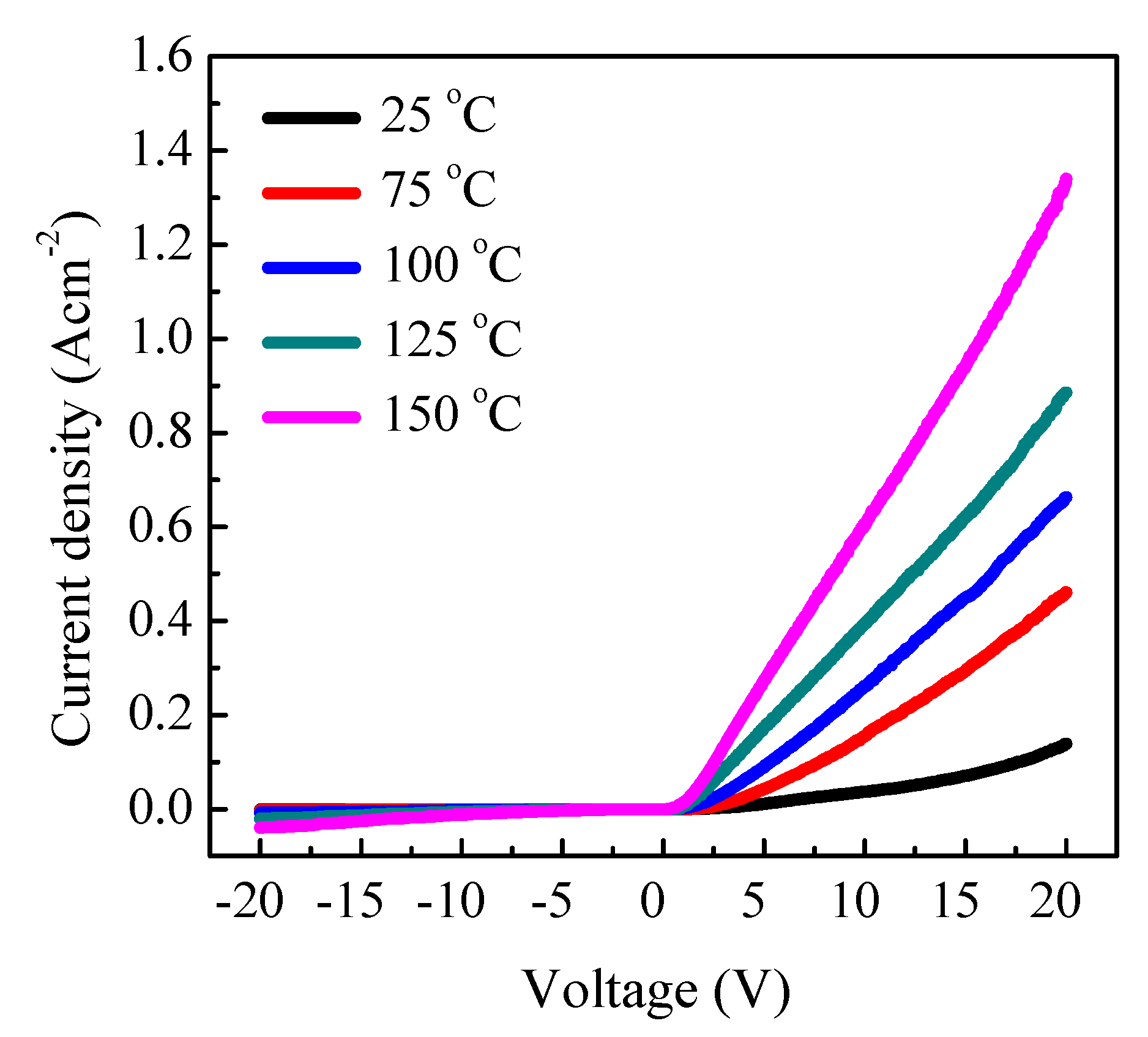
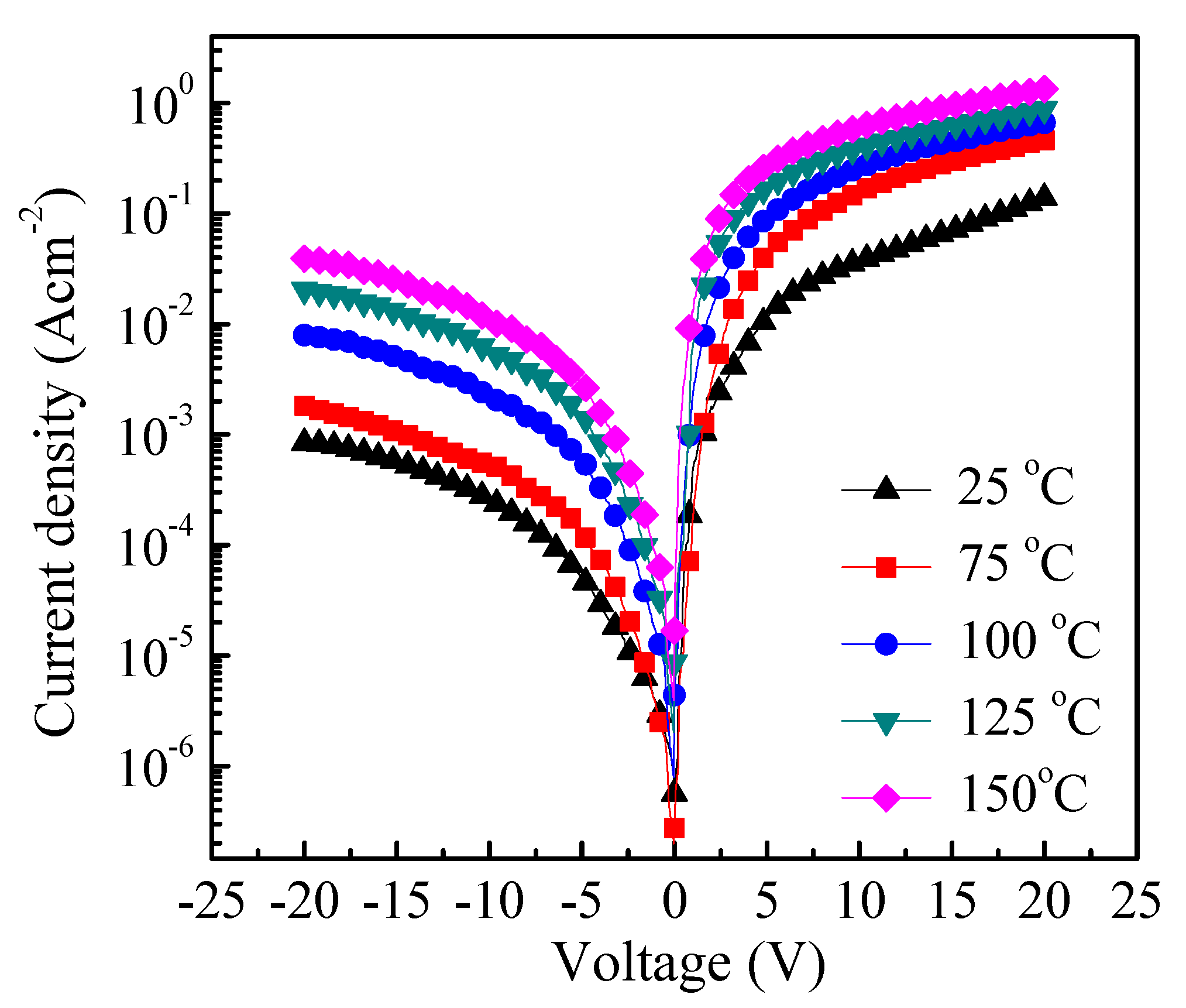
3.2. The p-Sb0.14GaN/n-Si heterojunction Diode
4. Conclusions
Author Contributions
Funding
Institutional Review Board Statement
Informed Consent Statement
Data Availability Statement
Acknowledgments
Conflicts of Interest
References
- Akasaki, I.; Amano, H. Crystal Growth and Conductivity Control of Group III Nitride Semiconductors and Their Application to Short Wavelength Light Emitters. Jpn. J. Appl. Phys. 1997, 36, 5393–5408. [Google Scholar] [CrossRef]
- Jain, S.C.; Willander, M.; Narayan, J.; Overstraeten, R.V. III-nitrides-Growth, characterization, and properties. J. Appl. Phys. 2000, 87, 965–1006. [Google Scholar] [CrossRef] [Green Version]
- Fujii, T.; Gao, Y.; Sharma, R.; Hu, E.L.; DenBaars, S.P.; Nakamura, S. Increase in the extraction efficiency of GaN-based light-emitting diodes via surface roughening. Appl. Phys. Lett. 2004, 84, 855–857. [Google Scholar] [CrossRef]
- Pearton, S.J.; Ren, F.; Zhang, A.P.; Lee, K.P. Fabrication and performance of GaN electronic devices. Mater. Sci. Eng. R Rep. 2000, 30, 205–212. [Google Scholar] [CrossRef]
- Rajan, S.; Chini, A.; Wong, M.H.; Speck, J.S.; Mishra, U.K. N-polar GaN/AlGaN/GaN high electron mobility transistors. J.Appl. Phys. 2007, 102, 044501. [Google Scholar] [CrossRef] [Green Version]
- Tuan, T.T.A.; Kuo, D.-H.; Li, C.C.; Yen, W.-C. Schottky barrier characteristics of Pt contacts to all sputtering-made n-type GaN and MOS diodes. J. Mater. Sci. Mater. Electron. 2014, 25, 3264–3270. [Google Scholar] [CrossRef]
- Tuan, T.T.A.; Kuo, D.-H.; Saragih, A.D.; Li, G.-Z. Electrical properties of RF-sputtered Zn-doped GaN films and p-Zn-GaN/n-Si hetero junction diode with low leakage current of 10−9A and a high rectification ratio above 105. Mater. Sci. Eng. B 2017, 222, 18–25. [Google Scholar] [CrossRef]
- Shuji, N. GaN Growth Using GaN Buffer Layer. Jpn. J. Appl. Phys. 1991, 30, L1705. [Google Scholar]
- Guarneros, C.; Sánchez, V. Magnesium doped GaN grown by MOCVD. Mater. Sci. Eng. B. 2010, 174, 263–265. [Google Scholar] [CrossRef]
- Akasaki, I.; Amano, H.; Koide, Y.; Hiramatsu, K.; Sawaki, N. Effects of ain buffer layer on crystallographic structure and on electrical and optical properties of GaN and Ga1-xAlxN (0 < x < 0.4) films grown on sapphire substrate by MOVPE. J. Crystal. Growth. 1989, 98, 209–219. [Google Scholar]
- Shota, K.; Kazumasa, H.; Nobuhiko, S. Fabrication of GaN Hexagonal Pyramids on Dot-Patterned GaN/Sapphire Substrates via Selective Metalorganic Vapor Phase Epitaxy. Jpn. J. Appl. Phys. 1995, 34, L1184. [Google Scholar]
- Hiroshi, A.; Masahiro, K.; Kazumasa, H.; Isamu, A. P-type Conduction in Mg-Doped GaN Treated with Low-Energy Electron Beam Irradiation (LEEBI). Japan. J. Appl. Phys. 1989, 28, L2112. [Google Scholar]
- Nakamura, S.; Harada, Y.; Seno, M. Novel metalorganic chemical vapor deposition system for GaN growth. Appl. Phys. Lett. 1991, 58, 2021–2023. [Google Scholar] [CrossRef]
- Shuji, N.; Takashi, M.; Masayuki, S.; Naruhito, I. Thermal Annealing Effects on P-Type Mg-Doped GaN Films. Jpn. J. Appl. Phys. 1992, 31, L139. [Google Scholar]
- Li, C.-C.; Kuo, D.-H. Material and technology developments of the totally sputtering-made p/n GaN diodes for cost-effective power electronics. J. Mater. Sci. Mater. Electron. 2014, 25, 1942–1948. [Google Scholar] [CrossRef]
- Thao, C.P.; Kuo, D.H. Electrical and structural characteristics of Ge-doped GaN thin films and its hetero-junction diode made all by RF reactive sputtering. Mater. Sci. Semicond. Process 2018, 74, 336–341. [Google Scholar] [CrossRef]
- Kuo, D.H.; Tuan, T.T.A.; Li, C.C.; Yen, W.C. Electrical and structural properties of Mg-doped InxGa1−xN (x ≤ 0.1) and p-InGaN/n-GaN junction diode made all by RF reactive sputtering. Mater. Sci. Eng. B 2015, 193, 18–25. [Google Scholar] [CrossRef]
- Thao, C.P.; Tuan, T.T.A.; Kuo, D.H.; Ke, W.C. Reactively Sputtered Sb-GaN Films and its Hetero-Junction Diode: The Exploration of the n-to-p Transition. Coatings 2020, 10, 210. [Google Scholar] [CrossRef] [Green Version]
- Thao, C.P.; Kuo, D.H.; Tuan, T.T.A.; Tuan, K.A.; Vu, N.H.; Via Sa Na, T.T.; Nhut, K.V.; Sau, N.V. The Effect of RF Sputtering Conditions on the Physical Characteristics of Deposited GeGaN Thin Film. Coatings 2019, 9, 645. [Google Scholar] [CrossRef] [Green Version]
- Li, C.C.; Kuo, D.H. Effects of growth temperature on electrical and structural properties of sputtered GaN films with a cermet target. J. Matter. Sci Mater. Electron. 2014, 25, 1404–1409. [Google Scholar] [CrossRef]
- Tuan, T.T.A.; Kuo, D.H. Characteristics of RF reactive sputter-deposited Pt/SiO2/n-InGaN MOS Schottky diodes. Mater. Sci. Semicond Process 2015, 30, 314–320. [Google Scholar] [CrossRef]
- Li, C.C.; Kuo, D.H.; Hsieh, P.W.; Huang, Y.S. Thick InxGa1−x N Films Prepared by Reactive Sputtering with Single Cermet Targets. J. Electron. Mater. 2013, 42, 2445–2449. [Google Scholar] [CrossRef]
- Kim, H.W.; Kim, N.H. Preparation of GaN films on ZnO buffer layers by RF magnetron sputtering. Appl. Sur. Sci. 2004, 236, 192–197. [Google Scholar] [CrossRef]
- Chyr, I.; Lee, B.; Chao, L.C.; Steckl, A.J. Damage generation and removal in the Ga+ focused ion beam micromachining of GaN for photonic applications. J. Vacuum. Sci. Tech. B 1999, 17, 3063–3067. [Google Scholar] [CrossRef]
- Yu, K.M.; Sarney, W.L.; Novikov, S.V.; Segercrantz, N.; Ting, M.; Shaw, M.; Svensson, S.P.; Martin, R.W.; Walukiewicz, W.; Foxon, C.T. Highly mismatched GaN1-xSbx alloys: Synthesis, structure and electronic properties. Semicond. Sci. Tech. 2016, 31, 083001. [Google Scholar] [CrossRef] [Green Version]
- Neugebauer, J.; Van de Walle, C.G. Atomic geometry and electronic structure of native defects in GaN. Phys. Rev. B 1994, 50, 8067–8070. [Google Scholar] [CrossRef] [PubMed]
- Mattila, T.; Nieminen, R.M. Point-defect complexes and broadband luminescence in GaN and AlN. Phys. Rev. B 1997, 55, 9571–9576. [Google Scholar] [CrossRef] [Green Version]
- Reddy, V.R.; Prasanna, B.P.; Padma, R. Electrical Properties of Rapidly Annealed Ir and Ir/Au Schottky Contacts on n-Type InGaN. J. Metall. 2012, 1, 1–9. [Google Scholar] [CrossRef] [Green Version]
- Cheung, S.K.; Cheung, N.W. Extraction of Schottky diode parameters from forward current-voltage characteristics. Appl. Phys. Lett. 1986, 49, 85–87. [Google Scholar] [CrossRef]
- Padma, R.; Reddy, V.R. Electrical Properties of Ir/n-InGaN/Ti/Al Schottky Barrier Diode in a Wide Temperature Range. Adv. Mater. Lett. 2014, 5, 31–38. [Google Scholar] [CrossRef]
- Lee, S.Y.; Kim, T.H.; Suh, D.I.; Park, J.E. An electrical characterization of a hetero-junction nanowire (NW) PN diode (n-GaN NW/pSi) formed by dielectrophoresis alignment. Phys. E 2007, 36, 194–198. [Google Scholar] [CrossRef]
- Cao, X.A.; Lachode, J.R.; Ren, F. Implanted p–n junction in GaN. Solid State Electron. 1999, 43, 1235–1238. [Google Scholar] [CrossRef]
- Hickman, R.; Vanhove, J.M.; Chow, P.P.; Klaassen, J.J. GaN PN junction issues and developments. Solid. State Electron. 2000, 44, 377–381. [Google Scholar] [CrossRef]
- Baik, K.H.; Irokawa, Y.; Ren, F.; Pearton, S.J.; Park, S.S.; Park, S.J. Temperature dependence of forward current characteristics of GaN junction and Schottky rectifiers. Solid State Electron. 2003, 47, 1533–1538. [Google Scholar] [CrossRef]
- Mohd, M.Z.; Baharin, A.; Hassan, Z.; Abu, H.; Abdullah, M.J. MBE growth of GaN pn-junction photodetector on AlN/Si substrate with Ni/Ag as Ohmic contact. Superlattices Microstruct. 2013, 56, 35–44. [Google Scholar] [CrossRef]
- Chirakkara, S.; Krupanidhi, S.B. Study of n-ZnO/p-Si(100) thin film heterojunctions by pulsed laser deposition without buffer layer. Thin Solid Films 2012, 520, 5894–5899. [Google Scholar] [CrossRef]
- Lin, K.; Kuo, D.H. Characteristics and electrical properties of reactively sputtered AlInGaN films from three different Al0.05InxGa0.95−xN targets with x = 0.075, 0.15, and 0.25. Mater. Sci. Semicond. Process. 2017, 57, 63–69. [Google Scholar] [CrossRef]
- Lin, K.; Kuo, D.H. Characterization of quaternary AlInGaN films obtained by incorporating Al into InGaN film with the RF reactive magnetron sputtering technology. J. Matter. Sci. Mater. Electron. 2017, 28, 43–51. [Google Scholar] [CrossRef]


| Temperature Deposition (°C) | Ga (at. %) | Sb (at. %) | N (at. %) | [Sb] /([Ga]+[Sb]) | [N] /([Ga]+[Sb]) |
|---|---|---|---|---|---|
| 100 | 46.48 | 3.24 | 50.28 | 0.065 | 1.011 |
| 200 | 46.31 | 3.91 | 49.78 | 0.078 | 0.991 |
| 300 | 45.89 | 4.92 | 49.19 | 0.097 | 0.968 |
| 400 | 45.64 | 5.23 | 49.13 | 0.103 | 0.966 |
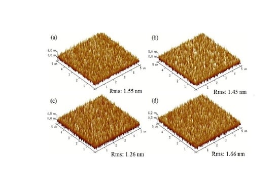
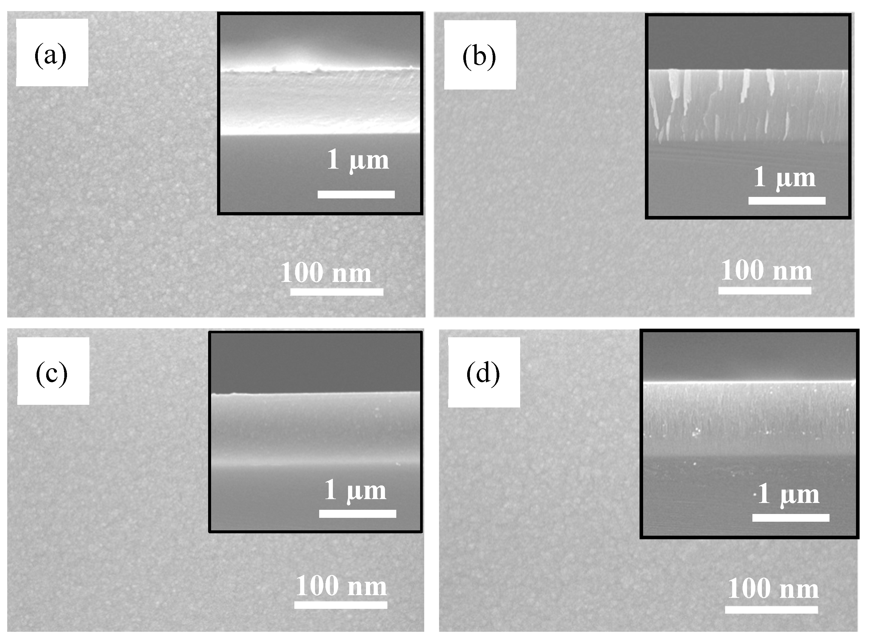
| Temperature Deposition (°C) | Film Thickness (µm) | Deposition Rate (nm/min) | Roughness (nm) |
|---|---|---|---|
| 100 | 1.00 | 33.33 | 1.55 |
| 200 | 1.13 | 37.67 | 1.45 |
| 300 | 1.17 | 39.00 | 1.26 |
| 400 | 1.24 | 41.33 | 1.66 |
| Temperature Deposition (°C) | 2θ | a (Å) | c (Å) | Volume (Å3) | (Degree) | Crystallite Size (nm) |
|---|---|---|---|---|---|---|
| 100 | 32.15 | 3.212 | 5.23 | 46.70 | 0.37 | 24 |
| 200 | 32.15 | 3.212 | 5.23 | 46.69 | 0.38 | 24 |
| 300 | 32.20 | 3.21 | 5.22 | 46.60 | 0.42 | 22 |
| 400 | 32.26 | 3.20 | 5.21 | 46.23 | 0.51 | 18 |
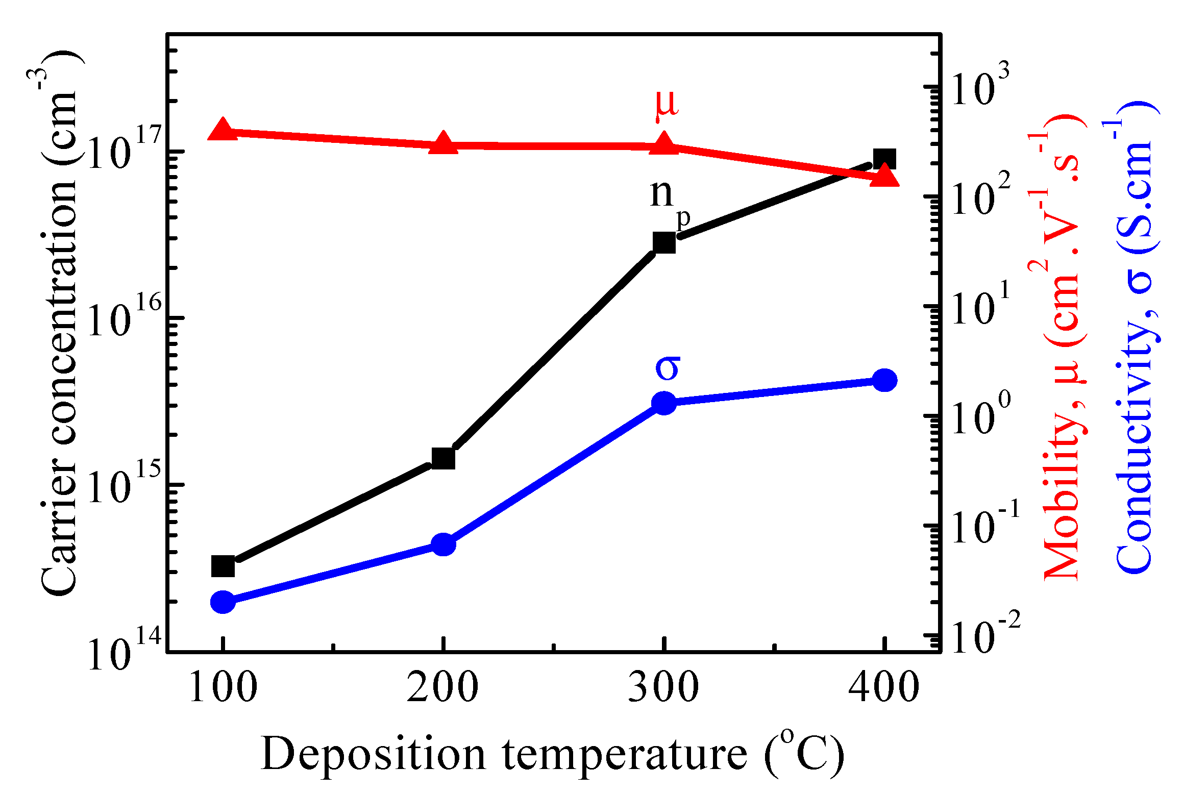
| Deposition Temperature (°C) | Type | Concentration Np cm−3 | Mobility µ cm2V−1s−1 | Conductivity σ Scm−1 |
|---|---|---|---|---|
| 100 | p | 3.25 × 10¹⁴ | 385 | 0.020 |
| 200 | p | 1.44 × 10¹⁵ | 289 | 0.067 |
| 300 | p | 2.83 × 10¹⁶ | 287 | 1.300 |
| 400 | p | 8.97 × 10¹⁶ | 146 | 2.100 |
| Samples | Leakage Current Density (A/cm2) at −5 V | Barrier Height (eV) | I-V | Cheungs’ dV/dlnI Versus I | |
|---|---|---|---|---|---|
| n | RS (kΩ) | n | |||
| 25 °C | 5.13 × 10⁻⁵ | 0.45 | 5.60 | 7.51 | 5.59 |
| 75 °C | 1.26 × 10⁻⁴ | 0.58 | 4.00 | 6.72 | 3.93 |
| 100 °C | 5.98 × 10⁻⁴ | 0.56 | 4.76 | 1.37 | 4.78 |
| 125 °C | 1.53 × 10⁻² | 0.54 | 5.31 | 0.53 | 5.36 |
| 150 °C | 2.96 × 10⁻² | 0.52 | 5.71 | 0.38 | 5.74 |
Publisher’s Note: MDPI stays neutral with regard to jurisdictional claims in published maps and institutional affiliations. |
© 2021 by the authors. Licensee MDPI, Basel, Switzerland. This article is an open access article distributed under the terms and conditions of the Creative Commons Attribution (CC BY) license (https://creativecommons.org/licenses/by/4.0/).
Share and Cite
Thao, C.P.; Kuo, D.-H.; Tuan, T.T.A. The Effect of RF Sputtering Temperature Conditions on the Structural and Physical Properties of Grown SbGaN Thin Film. Coatings 2021, 11, 752. https://doi.org/10.3390/coatings11070752
Thao CP, Kuo D-H, Tuan TTA. The Effect of RF Sputtering Temperature Conditions on the Structural and Physical Properties of Grown SbGaN Thin Film. Coatings. 2021; 11(7):752. https://doi.org/10.3390/coatings11070752
Chicago/Turabian StyleThao, Cao Phuong, Dong-Hau Kuo, and Thi Tran Anh Tuan. 2021. "The Effect of RF Sputtering Temperature Conditions on the Structural and Physical Properties of Grown SbGaN Thin Film" Coatings 11, no. 7: 752. https://doi.org/10.3390/coatings11070752
APA StyleThao, C. P., Kuo, D.-H., & Tuan, T. T. A. (2021). The Effect of RF Sputtering Temperature Conditions on the Structural and Physical Properties of Grown SbGaN Thin Film. Coatings, 11(7), 752. https://doi.org/10.3390/coatings11070752