Article

Optical and Structural Characterization of Cd-Free Buffer Layers Fabricated by Chemical Bath Deposition

1
Grupo de Investigación en Fotoquímica y Fotobiología, Facultad de Ciencias Básicas, Universidad del Atlántico, Puerto Colombia 081007, Colombia
2
Institución Universitaria Politécnico Gran Colombiano, Bogotá 110231, Colombia
*
Author to whom correspondence should be addressed.
Coatings 2021, 11(8), 897; https://doi.org/10.3390/coatings11080897
Submission received: 17 June 2021 / Revised: 21 July 2021 / Accepted: 24 July 2021 / Published: 27 July 2021
(This article belongs to the Special Issue Recent Advances in the Growth and Characterizations of Thin Films)

Abstract

:
Chemical bath deposition (CBD) is a suitable, inexpensive, and versatile synthesis technique to fabricate different semiconductors under soft conditions. In this study, we deposited Zn(O;OH)S thin films by the CBD method to analyze the effect of the number of thin film layers on structural and optical properties of buffer layers. Thin films were characterized by X-ray diffraction (XRD) and UV-Vis transmittance measurements. Furthermore, we simulated a species distribution diagram for Zn(O;OH)S film generation during the deposition process. The optical results showed that the number of layers determined the optical transmittance of buffer layers, and that the transmittance reduced from 90% (with one layer) to 50% (with four layers) at the visible range of the electromagnetic spectrum. The structural characterization indicated that the coatings were polycrystalline (α-ZnS and β-Zn(OH)2 to four layers). Our results suggest that Zn(O;OH)S thin films could be used as buffer layers to replace CdS thin films as an optical window in thin-film solar cells.

1. Introduction

Nowadays, the main primary energy source for electricity generation remains fossil fuels (oil, coal, natural gas), which are a non-renewable resource presenting a negative environmental impact due to emissions of greenhouse gases and other polluting by-products [1,2,3]. This traditional energy source does not warrant a long-term supply of the growing demand for energy created by population and industry growth [4,5,6]. This trend and the anthropogenic effect of human activities on the atmosphere, aquatic quality, and biodiversity are challenges for the near future [7,8]. This situation has generated great global interest in the search for new energy sources, preferably renewable ones. The Renewable Energy Police Network for the 21st Century (REN21) reported that 79.9% of the world’s total energy consumption was supplied by fossil fuels, 2.2% by nuclear energy, 6.9% by traditional biomass, and 11% by modern renewables (e.g., biomass/solar/geothermal heat (4.3%), hydropower (3.6%), wind/solar/biomass/ocean/geothermal power (2.1%), and biofuels for transport (1.0%). Among modern renewables, the global solar installed photovoltaic (PV) capacity grew more than 200 gigawatts (GW) in 2019 [9]. In the last 6 years, the increasing adoption rate of photovoltaic systems has also led to a price drop in excess of 80% [10]. Currently, crystalline silicon PV cells represent more than 85% of world PV cell market; however, the thin-film chalcogenide PV technology has shown a rapid growth compared to that of silicon due in part to its low cost of production [11]. The Cu(In,Ga)(Se,S)2 (CIGS) is one of the most researched materials as absorbent layers within thin-film PV technologies. In general, most of the CIGS-based solar cells include a very thin CdS (<100 nm) as a buffer layer to reduce crystalline mismatch between the chalcopyrite absorber layer and the transparent ZnO front electrode [12,13]. In the last two decades, serious efforts have been made to replace the CdS buffer layer by other nontoxic material [14,15,16]. Actually, in their last report, Green et al. reported an efficiency value of 23.3% for CIGS cells free of Cd [17]. Different compounds have been reported as alternatives to fabricate Cd-free buffer layers (e.g., ZnS [18], Zn(O,S) [15], ZnSe [19], In2S3 [20], CdS [21]). Among the semiconductor options, Zn(O,OH)S coatings are widely used as thin films in the fabrication of luminescent materials, light-emitting diodes, electroluminescent devices, optical covers, reflectors, and dielectric filters [22,23,24,25,26,27]. Since Zn(O;OH)S films have n-type conductivity and a large direct Eg bandgap (3.6–3.9 eV), they are suitable for use as buffer layers for thin-film solar cells [28].
Various deposition methods have been reported for the fabrication of semiconductor thin films: (i) thermal evaporation [29,30], (ii) sputtering [31], (iii) atomic layer deposition [32], (iv) electrochemical [33], (v) chemical vapor deposition [34], and (vi) chemical bath deposition (CBD) [35,36,37]. Among the physical and chemical methods of thin film deposition, the CBD process is the most economic and technically suitable one (e.g., regarding lab equipment and temperature and pressure requirements) [38]. In the typical procedure, with a temperature below that of the boiling point of water and under atmospheric pressure, a source of metal and chalcogenide are mixed in a vessel. First, temperature and pH are adjusted. Then, the solid substrate is immersed inside the reaction vessel, and the thin deposition starts. CBD is a convenient method for buffer layer deposition. However, thin film semiconductors grown using the CBD process produce large amounts of waste solvent and chemicals that then require costly waste processing [39]. The possibility of increasing optical transmission and deleting a toxic element (Cd) has directed the research in the field to study different synthesis parameters to optimize the CBD process (e.g., the effect of temperature, chalcogenide and metal source, complexing agents, pH, stirring). The main reports studied the physical–chemistry properties in thin films with only one coating (one layer) [40]. In this paper, we studied the effect of the number of buffer layers on the optical and structural properties of Zn(O;OH)S coatings deposited by CBD.

2. Materials and Methods

2.1. Thin Film Deposition by the CBD Process

Although the CBD process has been used in thin-film semiconductor synthesis for several decades, most reports do not explain the mechanism of film formation. Thus, different explanations have emerged, and two models are discussed in the literature to explain this process: (i) the ion–ion mechanism, which is a process that occurs by the direct reaction of the ions present in the solution on the surface of the substrate; and (ii) growth via cluster–cluster collisions. Figure 1a shows the ion–ion mechanism. In the first stage, the diffusion processes of metal ions (e.g., Zn2+ or In3+) and S2− ions occur on the surface of the substrate (Figure 1(a1)). In the second stage, the first semiconductor nuclei are generated on the surface of the substrate (Figure 1(a2)). In the third stage, the nuclei grow by adsorbing more ions, while new semiconductor nuclei are generated (Figure 1(a3)). Finally, the crystals grow and adhere to each other to generate the film (Figure 1(a4)) [41,42].
Figure 1b shows the cluster–cluster mechanism. In the first stage, colloidal size particles are generated in metal sulfide solution (e.g., ZnS or In2S3) or a possible intermediate (Zn(OH)2 or In(OH)3); then, these particles diffuse onto the substrate (Figure 1(bi)). In the second stage, the first nuclei are generated on the surface of the substrate (Figure 1(bii)). In the third stage, the nuclei grow by absorbing more Zn2+ and S2− ions, and the reaction continues until the possible intermediates transform into the respective sulfide through interchange reactions (Figure 1(biii)). Particle growth occurs both inside the solution and on the substrate surface. Finally, the particles adhere to each other on the surface of the substrate and form the film [41,42]. In the CBD process, both mechanisms may be present, generating the film and allowing the addition of colloidal aggregates for the subsequent growth of the film. The control of one of the two mechanisms is established by the extent of homogeneous and heterogeneous nucleation.
In the Zn(O;OH)S thin film deposition process, we used Thiourea as the S2+-ions source (150 mM), Zn acetate as the Zn2+-ions source (15 mM), and ammonia (350 mM) and sodium citrate (30 mM) as a complex agent with a temperature at 80 °C and pH at 10.5. In the CBD, soda-lime glass was used as substrate (SLG; 2 cm × 1.5 cm). After 45 min, the CBD was stoped, and the substrate was withdrawn and washed with distilled water. The thin layer was dried at ambient temperature. This first layer was immersed in a new chemical bath system, and the deposition process was repeated using this first layer as substrate to the second layer. This process was repeated to obtain different numbers of layers. Finally, the Zn(O;OH)S thin films were annealed in air at 400 °C for 30 min.

2.2. Thin Film Characterization

The thickness of the films was measured using a Veeco Dektak 150 profilometer (Plainview, NY, USA). The optical properties of the thin films were studied through transmittance measurements between 300 and 800 nm (Perkin Elmer Lambda 2S spectrophotometer, Waltham, MA, USA). The structural assay was carried out using a Shimadzu 6000 diffractometer (Tokyo, Japan) with a source of CuKα radiation (λ = 0.15418 nm) within the 2θ range of 20°–60°. Finally, the chemical surface assay was carried out using a Perkin-Elmer ESCA/SAM model 560 (Waltham, MA, USA).

3. Results and Discussion

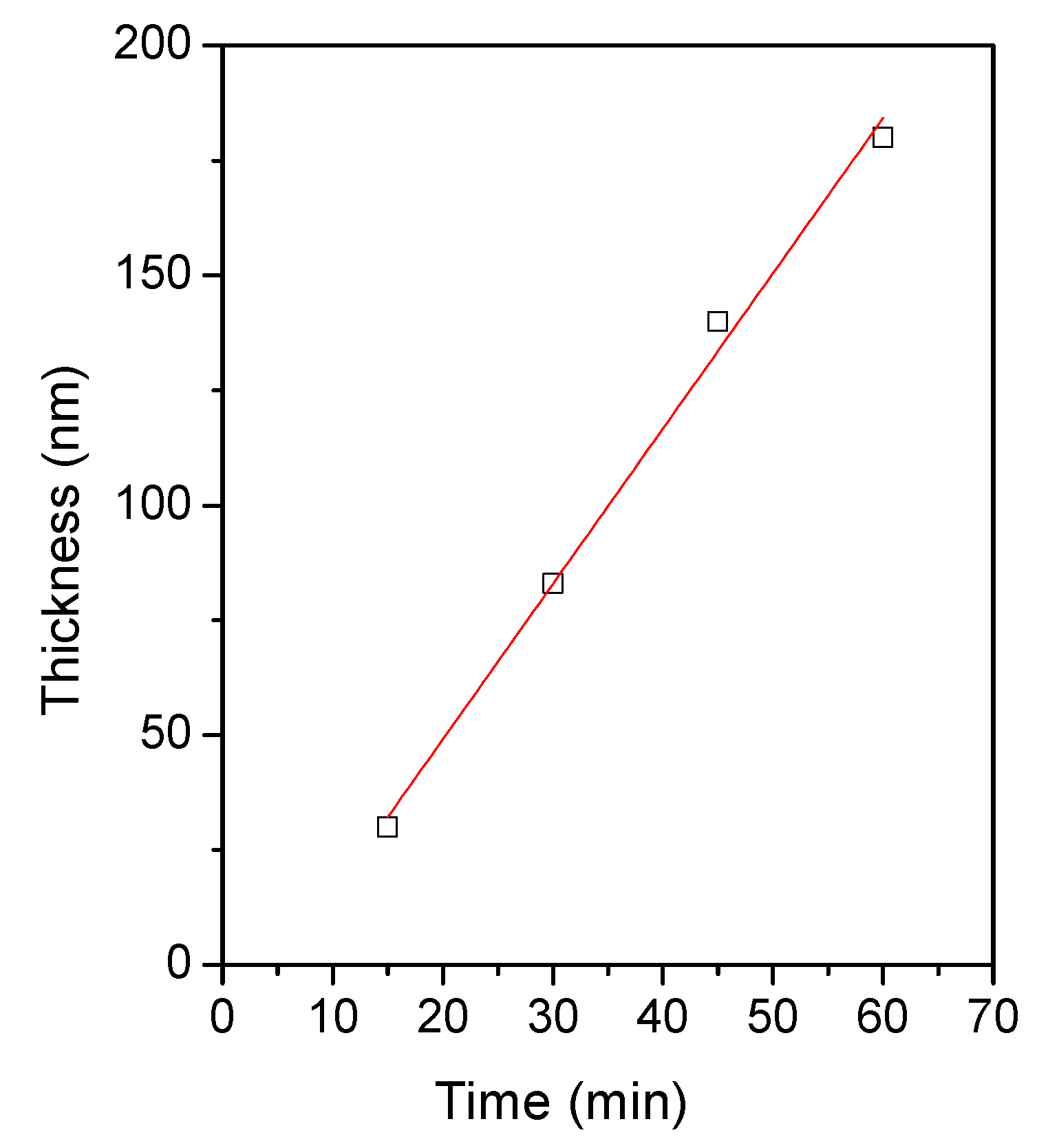
3.1. Thin Film Depostion

Figure 2 shows the Zn(O;OH)S thin-film thickness as a function of the deposition time. In the typical growth trend during CBD, two regions are distinguished: (a) linear growth, a stage in which the film thickness increases linearly with time, and (b) the saturation zone, a stage in which the growth rate decreases significantly as a consequence of consumption of the reagents inside the solution [43,44]. In our case, the data on thin film thickness within a 60 min time were suitable with linear fitting (R2 = 0.993); after this time, it is typical, in the CBD process, that linear kinetics change to due to the consumption of the reagents inside the solution. We performed the deposition of each layer within a 45-min deposition time (linear growth, Figure 2). Table 1 lists Zn(O;OH)S thin film thickness as a function of the number of layers. The results show a typical trend: as the number of layers increases, so does the thickness of the films. After the second layer, the coating thickness exceeds 100 nm. The typical thickness used to reduce the mechanical stress between the absorbent layer and the transparent conductor oxide (TCO) in thin-film solar cells is smaller than 100 nm. For three and four layers, the thickness values are 350 and 480 nm, respectively. The next sections will present the effect of the number of layers on the optical and structural thin films.
Although CBD is widely studied as a film deposition method, most reports are limited to exposing the different deposition parameters of the coatings; few reports show analytical studies about the chemical systems used during the deposition of the coatings. In a recent study, Gonzales et al. [45] reported the species distribution diagrams for CDB-ZnS film deposition. Due to chemical conditions (e.g., reagent concentration, pH, temperature), they did not report the formation of a ternary complex. It is known that the use of complexing agents reduces the homogeneous precipitation to obtain uniform and adherent coatings. The typical complexing agents in CBD include ammonia, hydrazine, ethanolamine, triethanolamine, tartaric acid, sodium citrate, and EDTA [46,47,48,49]. In the present study, we used sodium citrate to replace hydrazine in the CBD process. After CBD begins, the sulfide ion is generated as a free species in the solution due to hydrolysis of thiourea in a basic medium [50]:
SC(NH2)2 + OH → NCNH2 + SH(aq) + H2O.
Once the dissociated species of hydrogen sulfide (HS-) is formed in the medium, the S2−ion is formed as follows [50]:
SH + OH ⇋ S2−(aq) + H2O.
In the CBD solution, two solids can precipitate [50]:
Zn2+(aq) + S2−(aq) ⇋ ZnS(s)                      Ksp = 10−24.7
Zn2+(aq) + 2OH(aq) ⇋ Zn(OH)2(s)                      Ksp = 10−16
where Ksp is the solubility product constant (the equilibrium constant for the chemical equilibrium of solid dissolving in aqueous solution) [51]. The presence of a complexing agent is necessary to prevent the excessive formation of ZnS/Zn(OH)2. The complex formation reactions are as follows [52,53]:
Zn2+ +3Cit ⇋ [Zn(Cit)3]7−                       β = 105.5
Zn2+ + 4NH3 ⇋ [Zn(NH3)4]2+                       β = 109.46
Zn2+ + 4OH ⇋ [Zn(OH)4]2−                       β = 1015
[Zn(NH3)4]2+ + Cit ⇋ [Zn(NH3)3Cit] + NH3                       β = 1015
[Zn(NH3)3Cit] + Cit ⇋ [Zn(NH3)2(Cit)2]4− + NH3                       β = 1010
[Zn(NH3)2(Cit)2]4− + Cit ⇋ [Zn(NH3)(Cit)3]7− + NH3                       β = 107.46
where Cit represents citrate anion ([C6H5O7]3−), β is the stability constant (the equilibrium constant for the formation of the complex between metallic-ion and complexing agent) [51]. Based on the chemical equilibrium Equations (1)–(10) and single complexing equilibrium, we simulated the species distribution diagram for Zn(O;OH)S synthesized by the CBD. We calculated the fraction molar (xi) for each species at equilibrium, with the xi value being determined by physical–chemical conditions of the mixture (e.g., pH, reagent concentration, temperature). The theory and details of the methodology used to simulate the distribution diagram can be found in previous reports [54,55]. In the equation, xi represents the molar fraction of each species under specific chemical conditions, for which case we studied the pH effect on the xi value [45]:
x i = s i i s i     
where Si is the concentration of the species i at a specific pH. Regarding the stability constants of ternary compounds (4–6), Figure 3a shows the distribution diagram of the species involved in the thin films deposited by CBD in the pH range 2–14. Figure 3a shows that the hydroxyl complexes are important from pH values higher than 12. Furthermore, the complexing agent used (sodium citrate) participates in the generation of ternary complexes. Figure 3b shows that when under the pH conditions used during CBD (pH = 10–11), the ternary complexes (ammonium-Zn-citrate) are present (near 70% of the species in the CBD solution). Conventionally, CBD processes use hydrazine as a reducing and/or complexing agent due to its chemical and physical properties [56]. However, this compound poses serious risks for the environment and health. The challenge is to combine inexpensive and green chemical routes for semiconductor fabrication and to direct synthetic routes to develop hydrazine-free chemical bath depositions [57]. The results show that the chemical reagents used in CBD are suitable for Zn(O;OH)S thin-films synthesis; furthermore, the simulation indicates that the citrate complex acts as a complexing agent during CBD.

3.2. Structural Characterization

The effect of the number of thin film layers on structural properties was studied by X-ray diffraction. After the annealing procedure, the coatings with one and two layers did not show signals in the diffraction pattern (patterns are not shown), suggesting that these coatings could be formed by small-sized grains (on a nanoscopic scale); besides, the coatings with three and four layers were polycrystalline. Figure 4 shows the X-ray diffraction patterns for Zn(O;OH)S thin films (three and four layers).
Due to the chemical conditions of CBD, (i) the signals located at 2θ = 28.8°, 31.6°, 47.2°, and 58.2° were assigned to reflections of two different crystalline phases: (i) (002), (011), (110), and (0.21) planes of the hexagonal structure (Wurtzite; JCPDS 79-2204), and (ii) the signals located at 2θ = 28.8° and 47.2° were assigned to reflections of (111), (022) planes of the cubic structure (Zincblende; JCPDS 77-2100)) [58]. Furthermore, the signals located at 2θ = 34.4° and 58.22° were assigned to reflection β-Zn(OH)2 (JCPDS 77-2100) [59], and the presence of this signal suggests the formation of Zn(OH)2 or ZnO inside the buffer layer. The possible mechanism of generation and growth of the film occurs according to the formation of Zn(OH)2 (Equation (4)). This process is not eliminated from the reaction medium despite the fact that a low concentration of the metal ion and the addition of the complexing agent were used during CBD [50]. The competition between the formation of ZnS and Zn(OH)2 during the Zn-buffer layer deposition by CBD has been previously reported [45,60]. In a previous work [61], we identified that the Zn2+, sulfur, and oxygen were present inside the Zn(O;OH)S-thin films deposited by CBD, suggesting that ZnS and ZnO could be generated during the CBD process. Sáez-Araoz et al. [62] reported that in the early Zn-buffer layer deposition by CBD, a very thin film of ZnS is generated, which is followed by a mixture of ZnS and ZnO. Finally, other authors report the generation of a mixture of chemical phases during Zn-based buffer layers synthesized by CBD [63,64,65].

3.3. Optical Characterization

Figure 5a shows the transmittance curves of the Zn(O;OH)S films deposited on SLG by the CBD process. The number of layers significantly affected the spectral transmittance. In general, for one (90 nm) and two (190 nm) layers, transmittances are greater than 80% in the visible region of the electromagnetic spectrum (zone of low absorbance λ > 310 nm). Such a high transmittance value indicates that these coatings are optically suitable for use as a buffer layer. Furthermore, Figure 5a shows a deterioration in the optical transmittance for three and four layers, reducing until 60–70% (three layers) and 50–60% (four layers). High optical transmittance in the visible range of the electromagnetic spectrum is a critical requirement for buffer layers inside solar cells. The band-gap energy value was determined for all samples using the Tauc model. For films with reduced thickness and that do not present sufficient interference patterns, the absorption coefficient of each layer can be determined using the following equation [66,67]:
α h υ = 1 d L n 1 T h υ    
where α is the absorption coefficient, d corresponds to the thickness of the buffer layer and, T corresponds to the spectral transmittance as a function of the wavelength. The absorption coefficient is related to the band gap according to the following equation [68]:
α h υ = A ( h υ E g ) 2  
where Eg corresponds to the band gap of the material, and A is a constant. The value of Eg can be obtained by extrapolating the linear part of the graph of (αhν)2 vs. () to zero. This method was used to determine the Eg of the buffer layers. Figure 5b shows plots α2 versus (hv) for the transmittance spectra of Figure 5b. The optical band gap of the films was determined by extrapolating the linear portion of the graph onto the x-axis [68]. Table 1 lists the optical properties of the thin films. During the chemical bath deposition of semiconductors, it is common to produce a mixture of different chemical compounds [41,42]. In the case of Zn-buffer layers, depending on experimental parameters, the mixture of compounds (e.g., sulfide, hydroxide, and oxide) could be generated [69,70]. Furthermore, the semiconductor thin films band gap is affecting by thickness, crystalline structure, and physical–chemical composition [71,72]. The ZnO has a wide and direct band gap (≈3.37 eV) [73]. In the case of ZnS thin films, this is a semiconductor with a wide optical band gap (≈3.6 eV) [74,75]. However, the thin films band gap is affected by the deposition method and the post-treatment process. Mursal et al. [76], reported the optical band gap of ZnO thin films varying between 3.82 and 3.69 eV deposited by the sol–gel spin-coating method after changed the sintering temperature. The difference in the experimental and theorical band gap is attributed to the intrinsic defects in ZnO (e.g., O vacancy (VO), Zn vacancy (VZn), Zn interstitial (Zni), O interstitial (Oi) and anti-site Zn (ZnO)) [77,78,79]. Table 1 shows that the coating’s band gap changes between 3.65 and 3.81 eV. The band-gap energy of the Zn(O;OH)S coating synthesized by CBD has values between the band gap of ZnS and ZnO. This result could be related to the possibility of the generation of a mixture of chemical phases during buffer layers deposition (Section 3.2).
Furthermore, Table 1 shows that reducing the layer thickness affects the bulk properties and changes the optical properties, and that the thinner layers have a higher band-gap energy value, which is consistent with other reports. Das et al. reported band-gap variation with thickness for CdS thin films deposited by CBD and found that the band gap decreased from 3.2 eV (CdS thin films of 153 nm in thickness) until 2.54 eV (CdS thin films of 205 nm in thickness) [80]. Hossain et al. studied the In2S3 buffer layer band-gap variation from 2.0 to 2.9 eV to observe the effects thereof on electrical performance, and they reported that the band gap increased up to 2.9 eV with a layer of 50 nm in thickness, and this value decreased to 2.0 eV with a layer of 1 μm in thickness [81]. Such results verified that the number of layers in the coatings determines the physical–chemical properties of buffer layers (e.g., band gap, crystalline structure). Although all the coatings had energy values higher than 3.65 eV (requirement for the buffer layer in solar cells), only the coatings with one and two layers were suitable for use as buffer layers.

4. Conclusions

In this paper, we studied the structural and optical properties of Zn(O;OH)S coatings grown by CBD with different numbers of layers. We presented the simulation of the species distribution diagram for the Zn(O;OH)S synthesized by CBD. The thickness of the buffer layer films varied from 90 to 480 nm. The Zn(O;OH)S thin films with three and four layers represented a mixture of the cubic and hexagonal phases. Furthermore, the species diagram simulation indicates that the citrate complex could play an important role as a complexing agent during CBD. Finally, optical properties indicate that only the coatings with one and two layers were suitable for use as buffer layers, since these coatings had higher transmittance values. Furthermore, although all coatings had energy values higher than 3.65 eV, the coatings with three and four layers showed reduced transmittance in the visible region (50–70%).

Author Contributions

Conceptualization, W.V.; methodology, W.V., C.D.-U. and C.Q.; software, W.V.; validation, W.V., C.D.-U. and C.Q.; formal analysis, W.V., C.D.-U. and C.Q.; investigation, W.V.; resources, W.V.; data curation, W.V.; writing—original draft preparation, W.V., C.D.-U. and C.Q.; writing—review and editing, W.V., C.D.-U. and C.Q.; visualization, W.V.; supervision, W.V.; project administration, W.V.; funding acquisition, W.V. All authors have read and agreed to the published version of the manuscript.

Funding

This research was funded by Universidad del Atlántico RES. 002887.

Institutional Review Board Statement

Not applicable.

Informed Consent Statement

Not applicable.

Data Availability Statement

All data are contained within the article.

Acknowledgments

The authors thank Universidad del Atlántico.

Conflicts of Interest

The authors declare no conflict of interest.

References

  1. Vohra, K.; Vodonos, A.; Schwartz, J.; Marais, E.A.; Sulprizio, M.P.; Mickley, L.J. Global mortality from outdoor fine particle pollution generated by fossil fuel combustion: Results from GEOS-Chem. Environ. Res. 2021, 195, 110754. [Google Scholar] [CrossRef]
  2. Zhu, L.; Mickley, L.J.; Jacob, D.J.; Marais, E.A.; Sheng, J.; Hu, L.; Abad, G.G.; Chance, K. Long-term (2005–2014) trends in formaldehyde (HCHO) columns across North America as seen by the OMI satellite instrument: Evidence of changing emissions of volatile organic compounds. Geophys. Res. Lett. 2017, 44, 7079–7086. [Google Scholar] [CrossRef]
  3. Perera, F. Pollution from fossil-fuel combustion is the leading environmental threat to global pediatric health and equity: Solutions exist. Int. J. Environ. Res. Public Health 2018, 15, 16. [Google Scholar] [CrossRef] [PubMed] [Green Version]
  4. Dudley, B. BP Statistical Review of World Energy 2020; BP: London, UK, 2020. [Google Scholar]
  5. Martins, F.; Felgueiras, C.; Smitkova, M.; Caetano, N. Analysis of fossil fuel energy consumption and environmental impacts in european countries. Energies 2019, 12, 964. [Google Scholar] [CrossRef] [Green Version]
  6. Bebbington, J.; Schneider, T.; Stevenson, L.; Fox, A. Fossil fuel reserves and resources reporting and unburnable carbon: Investigating conflicting accounts. Crit. Perspect. Account. 2020, 66, 102083. [Google Scholar] [CrossRef]
  7. Ceballos, G.; Ehrlich, P.R.; Raven, P.H. Vertebrates on the brink as indicators of biological annihilation and the sixth mass extinction. Proc. Natl. Acad. Sci. USA 2020, 117, 13596–13602. [Google Scholar] [CrossRef]
  8. Bradshaw, C.J.A.; Ehrlich, P.R.; Beattie, A.; Ceballos, G.; Crist, E.; Diamond, J.; Dirzo, R.; Ehrlich, A.H.; Harte, J.; Harte, M.E.; et al. Underestimating the Challenges of Avoiding a Ghastly Future. Front. Conserv. Sci. 2021, 1, 615419. [Google Scholar] [CrossRef]
  9. REN21. Renewables 2020—Global Status Report; 2020 Update; REN21: Paris, France, 2020; ISBN 9783948393007. [Google Scholar]
  10. Castellanos, S.; Santibañez-Aguilar, J.E.; Shapiro, B.B.; Powell, D.M.; Peters, I.M.; Buonassisi, T.; Kammen, D.M.; Flores-Tlacuahuac, A. Sustainable silicon photovoltaics manufacturing in a global market: A techno-economic, tariff and transportation framework. Appl. Energy 2018, 212, 704–719. [Google Scholar] [CrossRef]
  11. Wilson, G.M.; Al-Jassim, M.; Metzger, W.K.; Glunz, S.W.; Verlinden, P.; Xiong, G.; Mansfield, L.M.; Stanbery, B.J.; Zhu, K.; Yan, Y.; et al. Exceeding 200 ns lifetimes in polycrystalline CdTe solar cells. Solar RRL 2020, 53, 493001. [Google Scholar]
  12. Lee, T.Y.; Lee, I.H.; Jung, S.H.; Chung, C.W. Characteristics of CdS thin films deposited on glass and Cu(In,Ga)Se2 layer using chemical bath deposition. Thin Solid Films 2013, 548, 64–68. [Google Scholar] [CrossRef]
  13. Merdes, S.; Malinen, V.; Ziem, F.; Lauermann, I.; Schüle, M.; Stober, F.; Hergert, F.; Papathanasiou, N.; Schlatmann, R. Zn(O,S) buffer prepared by atomic layer deposition for sequentially grown Cu(In,Ga)(Se,S)2 solar cells and modules. Sol. Energy Mater. Sol. Cells 2014, 126, 120–124. [Google Scholar] [CrossRef]
  14. Choubey, R.K.; Kumar, S.; Lan, C.W. Shallow chemical bath deposition of ZnS buffer layer for environmentally benign solar cell devices. Adv. Nat. Sci. Nanosci. Nanotechnol. 2014, 5, 025015. [Google Scholar] [CrossRef] [Green Version]
  15. Choi, W.J.; Park, W.W.; Kim, Y.; Son, C.S.; Hwang, D. The effect of AlD-Zn(O,S) buffer layer on the performance of CIGSSe thin film solar cells. Energies 2020, 13, 412. [Google Scholar] [CrossRef] [Green Version]
  16. Vallejo, W.; Quiñones, C.; Gordillo, G. A comparative study of thin films of Zn(O;OH)S and In(O;OH)S deposited on CuInS2 by chemical bath deposition method. J. Phys. Chem. Solids 2012, 73, 573–578. [Google Scholar] [CrossRef]
  17. Green, M.A.; Dunlop, E.D.; Hohl-Ebinger, J.; Yoshita, M.; Kopidakis, N.; Hao, X. Solar cell efficiency tables (version 56). Prog. Photovolt. Res. Appl. 2020, 28, 629–638. [Google Scholar] [CrossRef]
  18. Hong, J.; Lim, D.; Eo, Y.J.; Choi, C. Chemical bath deposited ZnS buffer layer for Cu(In,Ga)Se2 thin film solar cell. Appl. Surf. Sci. 2018, 432, 250–254. [Google Scholar] [CrossRef]
  19. Chen, Y.; Mei, X.; Liu, X.; Wu, B.; Yang, J.; Yang, J.; Xu, W.; Hou, L.; Qin, D.; Wang, D. Solution-processed CdTe thin-film solar cells using ZnSe nanocrystal as a buffer layer. Appl. Sci. 2018, 8, 1195. [Google Scholar] [CrossRef] [Green Version]
  20. Mughal, M.A.; Engelken, R.; Sharma, R. Progress in indium (III) sulfide (In2S3) buffer layer deposition techniques for CIS, CIGS, and CdTe-based thin film solar cells. Sol. Energy 2015, 120, 131–146. [Google Scholar] [CrossRef]
  21. Salomé, P.M.P.; Keller, J.; Törndahl, T.; Teixeira, J.P.; Nicoara, N.; Andrade, R.R.; Stroppa, D.G.; González, J.C.; Edoff, M.; Leitão, J.P.; et al. CdS and Zn1−xSnxOy buffer layers for CIGS solar cells. Sol. Energy Mater. Sol. Cells 2017, 159, 272–281. [Google Scholar] [CrossRef]
  22. Sabitha, C.; Joe, I.H.; Kumar, K.D.A.; Valanarasu, S. Investigation of structural, optical and electrical properties of ZnS thin films prepared by nebulized spray pyrolysis for solar cell applications. Opt. Quantum Electron. 2018, 50, 1–18. [Google Scholar] [CrossRef]
  23. Fathima, M.I.; Wilson, K.S.J. Antireflection coating application of zinc sulfide thin films by nebulizer spray pyrolysis technique. In AIP Conference Proceedings; AIP Publishing LLC: Melville, NY, USA, 2019; Volume 2115, p. 030327. [Google Scholar]
  24. Włodarski, M.; Chodorow, U.; Jóźwiak, S.; Putkonen, M.; Durejko, T.; Sajavaara, T.; Norek, M. Structural and optical characterization of ZnS ultrathin films prepared by low-temperature ALD from diethylzinc and 1.5-pentanedithiol after various annealing treatments. Materials 2019, 12, 3212. [Google Scholar] [CrossRef] [PubMed] [Green Version]
  25. Muchuweni, E.; Sathiaraj, T.S.; Nyakotyo, H. Synthesis and characterization of zinc oxide thin films for optoelectronic applications. Heliyon 2017, 3, e00285. [Google Scholar] [CrossRef] [Green Version]
  26. Shaban, M.; Zayed, M.; Hamdy, H. Nanostructured ZnO thin films for self-cleaning applications. RSC Adv. 2017, 7, 617–631. [Google Scholar] [CrossRef]
  27. Opasanont, B.; Van, K.T.; Kuba, A.G.; Choudhury, K.R.; Baxter, J.B. Adherent and conformal Zn(S,O,OH) thin films by rapid chemical bath deposition with hexamethylenetetramine additive. ACS Appl. Mater. Interfaces 2015, 7, 11516–11525. [Google Scholar] [CrossRef] [PubMed]
  28. Johnston, D.A.; Carletto, M.H.; Reddy, K.T.R.; Forbes, I.; Miles, R.W. Chemical bath deposition of zinc sulfide based buffer layers using low toxicity materials. In Proceedings of the Thin Solid Films; Elsevier: Amsterdam, The Netherlands, 2002; Volume 403–404, pp. 102–106. [Google Scholar]
  29. Memarian, N.; Rozati, S.M.; Concina, I.; Vomiero, A. Deposition of nanostructured Cds thin films by thermal evaporation method: Effect of substrate temperature. Materials 2017, 10, 773. [Google Scholar] [CrossRef]
  30. Kim, S.Y.; Rana, T.R.; Kim, J.H.; Yun, J.H. Cu(In,Ga)Se2 solar cells with In2S3 buffer layer deposited by thermal evaporation. J. Korean Phys. Soc. 2017, 71, 1012–1018. [Google Scholar] [CrossRef]
  31. Miliucci, M.; Lucci, M.; Colantoni, I.; De Matteis, F.; Micciulla, F.; Clozza, A.; Macis, S.; Davoli, I. Characterization of CdS sputtering deposition on low temperature pulsed electron deposition Cu(In,Ga)Se2 solar cells. Thin Solid Film. 2020, 697, 137833. [Google Scholar] [CrossRef]
  32. Ramanathan, K.; Mann, J.; Glynn, S.; Christensen, S.; Pankow, J.; Li, J.; Scharf, J.; Mansfield, L.; Contreras, M.; Noufi, R. A comparative study of Zn(O,S) buffer layers and CIGS solar cells fabricated by CBD, ALD, and sputtering. In Proceedings of the 2012 38th IEEE Photovoltaic Specialists Conference, Austin, TX, USA, 4 October 2012; pp. 1677–1680. [Google Scholar]
  33. Prabukanthan, P.; Harichandran, G. Electrochemical deposition of n-type ZnSe Thin Film Buffer Layer for Solar Cells. J. Electrochem. Soc. 2014, 161, D736–D741. [Google Scholar] [CrossRef]
  34. Palve, A.M. Deposition of zinc sulfide thin films from Zinc(II) thiosemicarbazones as single molecular precursors using aerosol assisted chemical vapor deposition technique. Front. Mater. 2019, 6, 46. [Google Scholar] [CrossRef] [Green Version]
  35. Li, J. Preparation and properties of CdS thin films deposited by chemical bath deposition. Ceram. Int. 2015, 41, S376–S380. [Google Scholar] [CrossRef]
  36. Maria, K.H.; Sultana, P.; Asfia, M.B. Chemical bath deposition of aluminum doped zinc sulfide thin films using non-toxic complexing agent: Effect of aluminum doping on optical and electrical properties. AIP Adv. 2020, 10, 65315. [Google Scholar] [CrossRef]
  37. Stumph, P.S.; Baranova, K.A.; Rogovoy, M.S.; Bunakov, V.V.; Maraeva, E.V.; Tulenin, S.S. Chemical bath deposition of In2S3 thin films as promising material and buffer layer for solar cells. In AIP Conference Proceedings; AIP Publishing LLC: Melville, NY, USA, 2019; Volume 2063, p. 040057. [Google Scholar]
  38. Aguilera, M.L.A.; Márquez, J.M.F.; Trujillo, M.A.G.; Kuwahara, Y.M.; Morales, G.R.; Galán, O.V. Influence of CdS thin films growth related with the substrate properties and conditions used on CBD technique. Energy Procedia 2014, 44, 111–117. [Google Scholar] [CrossRef] [Green Version]
  39. Chu, V.B.; Siopa, D.; Debot, A.; Adeleye, D.; Sood, M.; Lomuscio, A.; Melchiorre, M.; Guillot, J.; Valle, N.; El Adib, B.; et al. Waste- and Cd-free inkjet-printed Zn(O,S) buffer for Cu(In,Ga)(S,Se)2 thin-film solar cells. ACS Appl. Mater. Interfaces 2021, 13, 13009–13021. [Google Scholar] [CrossRef]
  40. Mugle, D.; Jadhav, G. Short review on chemical bath deposition of thin film and characterization. In AIP Conference Proceedings; AIP Publishing LLC: Melville, NY, USA, 2016; Volume 1728, p. 020597. [Google Scholar]
  41. Kashchiev, D. Nucleation Basic Theory with Applications, 1st ed.; Elsevier: Amsterdam, The Netherlands, 2000; ISBN 9780750646826. [Google Scholar]
  42. Hodes, G. Semiconductor and ceramic nanoparticle films deposited by chemical bath deposition. Phys. Chem. Chem. Phys. 2007, 9, 2181–2196. [Google Scholar] [CrossRef]
  43. Froment, M.; Lincot, D. Phase formation processes in solution at the atomic level: Metal chalcogenide semiconductors. Electrochim. Acta 1995, 40, 1293–1303. [Google Scholar] [CrossRef]
  44. Vallejo, W.; Clavijo, J.; Gordillo, G. CGS based solar cells with In2S3 buffer layer deposited by CBD and coevaporation. Braz. J. Phys. 2010, 40, 30–37. [Google Scholar] [CrossRef] [Green Version]
  45. González-Chan, I.J.; Oliva, A.I. Physicochemical analysis and characterization of chemical bath deposited zns films at near ambient temperature. J. Electrochem. Soc. 2016, 163, D421–D427. [Google Scholar] [CrossRef]
  46. Goudarzi, A.; Aval, G.M.; Sahraei, R.; Ahmadpoor, H. Ammonia-free chemical bath deposition of nanocrystalline ZnS thin film buffer layer for solar cells. Thin Solid Films 2008, 516, 4953–4957. [Google Scholar] [CrossRef]
  47. Lǎdar, M.; Popovici, E.J.; Baldea, I.; Grecu, R.; Indrea, E. Studies on chemical bath deposited zinc sulphide thin films with special optical properties. J. Alloy. Compd. 2007, 434–435, 697–700. [Google Scholar] [CrossRef]
  48. Karakawa, M.; Sugahara, T.; Hirose, Y.; Suganuma, K.; Aso, Y. Thin film of amorphous zinc hydroxide semiconductor for optical devices with an energy-efficient beneficial coating by metal organic decomposition process. Sci. Rep. 2018, 8, 10839. [Google Scholar] [CrossRef] [PubMed]
  49. Rodríguez, C.A.; Flores, M.; Sandoval-Paz, M.; Delplancke, M.P.; Cabello-Guzmán, G.; Carrasco, C. Study of the early growth stages of chemically deposited ZnS thin films from a non-toxic solution. Mater. Res. Express 2018, 5, 076404. [Google Scholar] [CrossRef]
  50. Oladeji, I.O.; Chow, L. A study of the effects of ammonium salts on chemical bath deposited zinc sulfide thin films. Thin Solid Films 1999, 339, 148–153. [Google Scholar] [CrossRef]
  51. Wagh, A.S. Dissolution Characteristics of Metal Oxides and Kinetics of Ceramic Formation. In Chemically Bonded Phosphate Ceramics; Elsevier: Amsterdam, The Netherlands, 2016; pp. 61–73. [Google Scholar]
  52. Meites, L. Handbook of Analytical Chemistry, 1st ed.; McGraw-Hill: New York, NY, USA, 1963. [Google Scholar]
  53. Clavijo Díaz, A. Fundamentos de Química Analítica: Equilibrio Iónico y Análisis Químico; Universidad Nacional de Colombia: Bogotá, Colombia, 2002; Volume 1. [Google Scholar]
  54. González-Panzo, I.J.; Martín-Várguez, P.E.; Oliva, A.I. Physicochemical conditions for ZnS films deposited by chemical bath. J. Electrochem. Soc. 2014, 161, D181–D189. [Google Scholar] [CrossRef]
  55. Reinisch, M.; Perkins, C.L.; Steirer, K.X. Quantitative study on the chemical solution deposition of zinc oxysulfide. ECS J. Solid State Sci. Technol. 2016, 5, P58–P66. [Google Scholar] [CrossRef]
  56. Kim, J. Comparison of ZnS film growth on glass and CIGS substrates via hydrazine-assisted chemical bath deposition for solar cell application. Appl. Sci. Converg. Technol. 2019, 28, 229–233. [Google Scholar] [CrossRef]
  57. Guerrero, G.A.; Rodríguez, A.G.; Moreno-García, H. Hydrazine-free chemical bath deposition of WSe2 thin films and bi-layers for photovoltaic applications. Mater. Res. Express 2019, 6, 105906. [Google Scholar] [CrossRef]
  58. Zhao, H.; Liu, W.; Zhu, J.; Shen, X.; Xiong, L.; Li, Y.; Li, X.; Liu, J.; Wang, R.; Jin, C.; et al. Structural transition behavior of ZnS nanotetrapods under high pressure. High Press. Res. 2015, 35, 9–15. [Google Scholar] [CrossRef]
  59. Mousavi-Kamazani, M.; Zinatloo-Ajabshir, S.; Ghodrati, M. One-step sonochemical synthesis of Zn(OH)2/ZnV3O8 nanostructures as a potent material in electrochemical hydrogen storage. J. Mater. Sci. Mater. Electron. 2020, 31, 17332–17338. [Google Scholar] [CrossRef]
  60. Hubert, C.; Naghavi, N.; Etcheberry, A.; Roussel, O.; Hariskos, D.; Powalla, M.; Kerrec, O.; Lincot, D. A better understanding of the growth mechanism of Zn(S,O,OH) chemical bath deposited buffer layers for high efficiency Cu(In,Ga)(S,Se)2 solar cells. Phys. Status Solidi 2008, 205, 2335–2339. [Google Scholar] [CrossRef]
  61. Vallejo, W.; Diaz-Uribe, C.; Hurtado, M. Caracterización fisicoquímica del sistema Mo/CuInS2/Zn(O,OH)S/ZnO por medio de espectroscopía fotoelectrónica XPS y AES. Elementos 2014, 4. [Google Scholar] [CrossRef] [Green Version]
  62. Sáez-Araoz, R.; Abou-Ras, D.; Niesen, T.P.; Neisser, A.; Wilchelmi, K.; Lux-Steiner, M.C.; Ennaoui, A. In situ monitoring the growth of thin-film ZnS/Zn(S,O) bilayer on Cu-chalcopyrite for high performance thin film solar cells. Thin Solid Film. 2009, 517, 2300–2304. [Google Scholar] [CrossRef]
  63. Buffière, M.; Harel, S.; Arzel, L.; Deudon, C.; Barreau, N.; Kessler, J. Fast chemical bath deposition of Zn(O,S) buffer layers for Cu(In,Ga)Se2 solar cells. Thin Solid Film. 2011, 519, 7575–7578. [Google Scholar] [CrossRef]
  64. Ennaoui, A.; Siebentritt, S.; Lux-Steiner, M.C.; Riedl, W.; Karg, F. High-efficiency Cd-free CIGSS thin-film solar cells with solution grown zinc compound buffer layers. Sol. Energy Mater. Sol. Cells 2001, 67, 31–40. [Google Scholar] [CrossRef]
  65. Platzer-Björkman, C.; Törndahl, T.; Abou-Ras, D.; Malmström, J.; Kessler, J.; Stolt, L. Zn(O,S) buffer layers by atomic layer deposition in Cu(In,Ga)Se2 based thin film solar cells: Band alignment and sulfur gradient. J. Appl. Phys. 2006, 100, 044506. [Google Scholar] [CrossRef]
  66. Makuła, P.; Pacia, M.; Macyk, W. How to correctly determine the band gap energy of modified semiconductor photocatalysts based on UV-Vis spectra. J. Phys. Chem. Lett. 2018, 9, 6814–6817. [Google Scholar] [CrossRef] [PubMed] [Green Version]
  67. Escobedo-Morales, A.; Ruiz-López, I.I.; Ruiz-Peralta, M.D.; Tepech-Carrillo, L.; Sánchez-Cantú, M.; Moreno-Orea, J.E. Automated method for the determination of the band gap energy of pure and mixed powder samples using diffuse reflectance spectroscopy. Heliyon 2019, 5, e01505. [Google Scholar] [CrossRef] [Green Version]
  68. Viezbicke, B.D.; Patel, S.; Davis, B.E.; Birnie, D.P. Evaluation of the tauc method for optical absorption edge determination: ZnO thin films as a model system. Phys. Status Solidi 2015, 252, 1700–1710. [Google Scholar] [CrossRef]
  69. Wang, L.P.; De Han, P.; Zhang, Z.X.; Zhang, C.L.; Xu, B.S. Effects of thickness on the structural, electronic, and optical properties of MgF2 thin films: The first-principles study. Comput. Mater. Sci. 2013, 77, 281–285. [Google Scholar] [CrossRef] [Green Version]
  70. Zhou, L.; Xue, Y.; Li, J. Study on ZnS thin films prepared by chemical bath deposition. J. Environ. Sci. 2009, 21, S76–S79. [Google Scholar] [CrossRef]
  71. Chaves, A.; Azadani, J.G.; Alsalman, H.; da Costa, D.R.; Frisenda, R.; Chaves, A.J.; Song, S.H.; Kim, Y.D.; He, D.; Zhou, J.; et al. Bandgap engineering of two-dimensional semiconductor materials. Npj 2D Mater. Appl. 2020, 4, 29. [Google Scholar] [CrossRef]
  72. Gong, Y.; Liu, Z.; Lupini, A.R.; Shi, G.; Lin, J.; Najmaei, S.; Lin, Z.; Elías, A.L.; Berkdemir, A.; You, G.; et al. band gap engineering and layer-by-layer mapping of selenium-doped molybdenum disulfide. Nano Lett. 2013, 14, 442–449. [Google Scholar] [CrossRef]
  73. Kamarulzaman, N.; Kasim, M.F.; Rusdi, R. Band gap narrowing and widening of ZnO nanostructures and doped materials. Nanoscale Res. Lett. 2015, 10, 346. [Google Scholar] [CrossRef] [PubMed] [Green Version]
  74. D’Amico, P.; Calzolari, A.; Ruini, A.; Catellani, A. New energy with ZnS: Novel applications for a standard transparent compound. Sci. Rep. 2017, 7, 16805. [Google Scholar] [CrossRef] [PubMed]
  75. Jiang, P.; Jie, J.; Yu, Y.; Wang, Z.; Xie, C.; Zhang, X.; Wu, C.; Wang, L.; Zhu, Z.; Luo, L. Aluminium-doped n-type ZnS nanowires as high-performance UV and humidity sensors. J. Mater. Chem. 2012, 22, 6856–6861. [Google Scholar] [CrossRef]
  76. Jalil, Z. Structural and optical properties of zinc oxide (ZnO) based thin films deposited by sol-gel spin coating method. J. Phys. Conf. Ser. 2018, 1116, 032020. [Google Scholar]
  77. Xiu, F.; Xu, J.; Joshi, P.C.; Bridges, C.A.; Paranthaman, M.P. ZnO doping and defect engineering—A review. Springer Ser. Mater. Sci. 2016, 218, 105–140. [Google Scholar]
  78. Lyons, J.L.; Varley, J.B.; Steiauf, D.; Janotti, A.; Walle, C.G. Van de first-principles characterization of native-defect-related optical transitions in ZnO. J. Appl. Phys. 2017, 122, 035704. [Google Scholar] [CrossRef]
  79. Liang, Y.-C.; Hung, C.-S.; Zhao, W.-C. Thermal annealing induced controllable porosity and photoactive performance of 2D ZnO sheets. Nanomaterials 2020, 10, 1352. [Google Scholar] [CrossRef]
  80. Das, N.S.; Ghosh, P.K.; Mitra, M.K.; Chattopadhyay, K.K. Effect of film thickness on the energy band gap of nanocrystalline CdS thin films analyzed by spectroscopic ellipsometry. Phys. E Low-Dimens. Syst. Nanostruct. 2010, 42, 2097–2102. [Google Scholar] [CrossRef]
  81. Istiaque Hossain, M.; Chelvanathan, P.; Zaman, M.; Karim, M.R.; Alghoul, M.A.; Amin, N. Prospects of indium sulphide as an alternative to cadmium sulphide buffer layer in CIS based solar cells from numerical analysis. Chalcogenide Lett. 2011, 8, 315–324. [Google Scholar]
Figure 1. (a) Schematic diagram of the ion–ion mechanism: (1) Ion diffusion (M+ represents Zn2+ or In3+) from bulk solution to substrate surface. (2) Heterogeneous nucleation on the substrate surface and crystal growth on substrate surface. (3) Coalescence and growth of films. (b) Cluster–cluster mechanism: (i) metal sulfide and metal hydroxide particle formation into bulk solution, followed by solid particle diffusion to substrate surface. (ii) Diffusion of sulfide ions and reaction with solid particles located on the substrate surface and crystal growth by interchange reactions (metal hydroxide) and by sulfide addition (metal sulfide). (iii) Particle growth occurs both inside the solution and on the substrate surface. Bars represent solid substrates.
Coatings 11 00897 g001
Figure 2. Zn(O;OH)S thin-film thickness as a function of CBD deposition time. White squares represent data and the red line represents the linear fitting. Fitting data: R2 = 0.993. Fitting equation: y = 3.38(x) − 18.5.
Coatings 11 00897 g002
Figure 3. Species distribution diagram for Zn(O;OH)S synthesized by the CBD method under experimental conditions. (a) pH range 2–14. (b) zoom range pH 10–12. Inside figure, Cit represents citrate anion ([C6H5O7]3−). (xi) represents fraction molar for each species at equilibrium.
Coatings 11 00897 g003
Figure 4. X-ray diffraction patterns of Zn(O;OH)S-thin film thickness as a function of the number of the layers. (a) Zn(O;OH)S coatings three layers. (b) Zn(O;OH)S coatings four layers. Inside figure: (*) The signal could be assigned to Wurtzite and/or Zincblende structure. (l) The signal could be assigned to Zn(OH)2 structure.
Coatings 11 00897 g004
Figure 5. (a) Zn(O;OH)S thin-film transmittance as a function of the number of layers deposited by CBD. (b) Tauc plots and band-gap energy estimation for the Zn(O;OH)S thin films as a function of the number of layers deposited by CBD.
Coatings 11 00897 g005
Table 1. Optical and structural properties of the thin films, varying the number of layers deposited by CBD.
Number LayersThickness (nm)Energy Band Gap (eV) 1Crystal Properties
1903.81Amorphous
21903.77Amorphous
33503.70Cubic/hexagonal phases
44803.65Cubic/hexagonal phases
1 Value as a result of extrapolating the linear portion of the graph onto the x-axis in Figure 5b.
Publisher’s Note: MDPI stays neutral with regard to jurisdictional claims in published maps and institutional affiliations.

