Article

Based on Ultrathin PEDOT:PSS/c-Ge Solar Cells Design and Their Photoelectric Performance

1
Joint Laboratory for Extreme Conditions Matter Properties, Southwest University of Science and Technology, Mianyang 621010, China
2
State Key Laboratory of Advanced Processing and Recycling of Non-ferrous Metals, Lanzhou University of Technology, Lanzhou 730050, China
3
School of Science, Huzhou University, Huzhou 313000, China
4
College of Science, Zhejiang University of Technology, Hangzhou 310023, China
5
Fujian Provincial Key Laboratory for Advanced Micro-Nano Photonics Technology and Devices, Quanzhou Normal University, Quanzhou 362000, China
6
Key Laboratory of Microelectronic Devices & Integrated Technology, Institute of Microelectronics, Chinese Academy of Sciences, Beijing 100029, China
*
Authors to whom correspondence should be addressed.
Coatings 2021, 11(7), 748; https://doi.org/10.3390/coatings11070748
Submission received: 12 May 2021 / Revised: 8 June 2021 / Accepted: 18 June 2021 / Published: 22 June 2021
(This article belongs to the Special Issue Micro-Nano Optics and Its Applications)

Abstract

:
In recent years, nanostructures have improved the performance of solar cells and are regarded as the most promising microstructures. The optical properties of PEDOT:PSS/c-Ge hybrid solar cells (HSCs) based on the octagon germanium nanoparticles (O-GNPs) were numerically analyzed using the finite-difference time-domain (FDTD) method. The optimal structure of the hybrid solar cell is determined by changing the thickness of the organic layer and structural parameters of nanoparticles to enhance the optical absorption and eventually achieve high broadband absorption. By changing the structure parameter of O-GNPs, we studied its effect on solar cells. The optimization of geometric parameters is based on maximum absorption. The light absorption of our optimized HSCs is basically above 90% between 200 and 1500 nm. PEDOT:PSS is placed on top of O-GNPs to transmit the holes better, allowing O-GNPs to capture a lot of photons, to increase absorbance value properties in the AM1.5 solar spectral irradiated region. The transmittance is increased by adding poly-methyl methacrylate (PMMA). At the same time, the electrical characteristics of Ge solar cells were simulated by DEVICE, and short-circuit current (Jsc), open-circuit voltage (Voc), maximum power (Pmax), filling coefficient (FF) and photoelectric conversion efficiency (PCE) were obtained. According to the optimization results after adjusting the structural parameters, the maximum short-circuit current is 44.32 mA/cm2; PCE is 7.84 mW/cm2; FF is 69%. The results show that the O-GNPs have a good light trapping effect, and the structure design has great potential for the absorption of HSCs; it is believed that the conversion efficiency will be further improved through further research.

1. Introduction

With the continuous development of the social economy and the continuous progress of human civilization, the human demand for energy has been developing rapidly. As a kind of environmental protection and pollution-free renewable energy, solar energy has been widely developed and utilized by human beings [1,2,3,4]. Converting solar energy into other forms of energy is already well established. One obvious aspect is the conversion of solar energy into electricity, namely solar cells, which not only saves costs but also greatly reduces the waste of resources. How to develop efficient solar cells has become a hot research topic [5,6,7]. Germanium, as the second-generation semiconductor, has remarkable advantages. Crystalline germanium (c-Ge), as the substrate and bottom cell of multijunction solar cells, can effectively make use of photo-generated carriers and improve the efficiency of solar cells [8,9]. Ge-based multijunction solar cells are used in space and concentrator photovoltaics (CPV) applications [10,11]. Ge solar cells have also been used in thermal and photovoltaic applications [12,13,14]. Ultrathin hydrogenated amorphous Ge (a-Ge:H) absorbent with ultrathin resonator-reinforced solar cells can replace microcrystalline silicon-absorbent Si thin-film solar cells with a thick micron [15]. Bahman prepared high-efficiency heterojunction solar cells with a conversion productivity of 5.9% and 7.2%, respectively, on n-type and P-type crystal Ge substrates [16]. Ge was used for the bottom cell, and Ga(ln)As was used for the middle cell; the maximum open-circuit voltage of the three-junction solar cell reached 25 mV [17].
Although Ge-based solar cells have good performance, the development of Ge-based solar cells in the ground photovoltaic market is limited due to its low crustal content and high manufacturing cost. In the aspect of solar cells, in addition to the Ge solar cells mentioned above, polymer solar cells are also a major research direction. Polymer solar cells have become a hotspot in the research of solar cells due to their advantages such as a simple fabrication process, light weight, cost effectiveness and convenient production of massive area flexible devices [18]. In recent years, great progress has been made in the research of polymer solar cells [19,20]. In polymer materials, organic poly (3,4-ethylene-dioxythiophene):poly(styrenesulfonate) (PEDOT:PSS) is widely studied and applied in many fields due to its high conductivity, high stability and good light transmittance [21,22]. However, there are still problems of low efficiency and poor stability in current polymer solar cells, which make it difficult to popularize and use. Indium Tin Oxide semiconductor transparent conductive film (ITO), with good conductivity and transparency [23,24,25], and the combination of ITO and PEDOT:PSS, can enhance the conductivity of PEDOT:PSS [26,27]. ITO stacks on PEDOT:PSS, and then a tunneling effect occurs between the two, forming an ohmic contact [28]. PEDOT:PSS is the carrier layer for carriers, which pass through the organic layer quickly, while the ITO layer plays a good role in collecting carriers [29], and plays the role of the optical window and anti-reflection layer [30,31]. In order to improve the performance of polymer solar cells further, recently the combination of polymer and semiconductor material solar cells has been widely studied because it can make up for the low efficiency of polymer solar cells. Lu et al. proposed that the absorption of Si/PEDOT:PSS core/shell nanowire arrays for efficient hybrid solar cells is about 88%, and the PCE reaches 6.35% [32]. Mariani proposed a core-shell hybrid solar cell with a PCE of 4.11% by coating PEDOT on GaAs nanocolumn arrays and adding dopants to the polymer [33]. At present, the research on hybrid solar cells has been very advanced, but its limitation is that the conversion efficiency is not high, and the photoelectric performance of solar cells needs to be improved.
Nanostructures are one of the main methods to improve the efficiency of photovoltaic cells. Due to their good permeability and optical capture performance, they have a good light-trapping effect and increase the photocurrent of solar cells, which has generated plenty of studies [34,35]. For example, the photocurrent of the same thin-film Si solar cell was increased by 5% by using the nanometer column compared with the Ag backplate [36]. Ge quantum dots in the long wavelength range (>600 nm) can significantly improve the quantum efficiency of crystalline Si solar cells, and increase the short-circuit current by 3.3% (compared with without Ge quantum dots) [37]. There has been a recent flurry of polymer deposition on nanoparticles, and the short-circuit current of the combined solar cells has been greatly increased. The short-circuit current of the InP-based truncated nanoparticle solar cell with the PEDOT:PSS conformation coating was 24.73% [38]. PEDOT:PSS/c-Si hybrid solar cell based on metal nanoparticles has a short-circuit current of 41.71% [39]. However, there are few studies on high-efficiency solid Ge nanoparticles combined with PEDOT:PSS. Ge is suitable for binding to PEDOT:PSS as a receptor material because of its good electron affinity, which can improve the generation, separation and transport of photons [40,41].Therefore, the absorption efficiency of the solar cell was studied by establishing a Ge-based octagonal nanoparticle binding model with the organic active layer.
In this article, O-GNPs were placed in PEDOT:PSS to enhance optical absorption, light capture, short-circuit current and open-circuit voltage of Ge solar cells at higher wavelengths. We studied the light absorption and short-circuit current of PEDOT:PSS/c-Ge HSCs by adding the excellent properties of nanoparticles and obtained a wideband high absorption curve and a high short-circuit current value. Its optical and electrical properties can be calculated by FDTD and DEVICE software, respectively. The effects of the height and width of O-GNPs on the light absorption of solar cells were studied. By changing the thickness of O-GNPs and the active layer of PEDOT:PSS, the relationship between the light-absorption efficiency, electric field intensity, open-circuit voltage and transformation efficiency of the active layer and the nanoparticles with different thicknesses was obtained. We also studied the light transmittance of different thickness ratios of the optical window SiO2 and PMMA. Finally, the results show that the PEDOT:PSS/c-Ge hybrid solar cells with O-GNPs have a higher photocurrent than those previously studied.

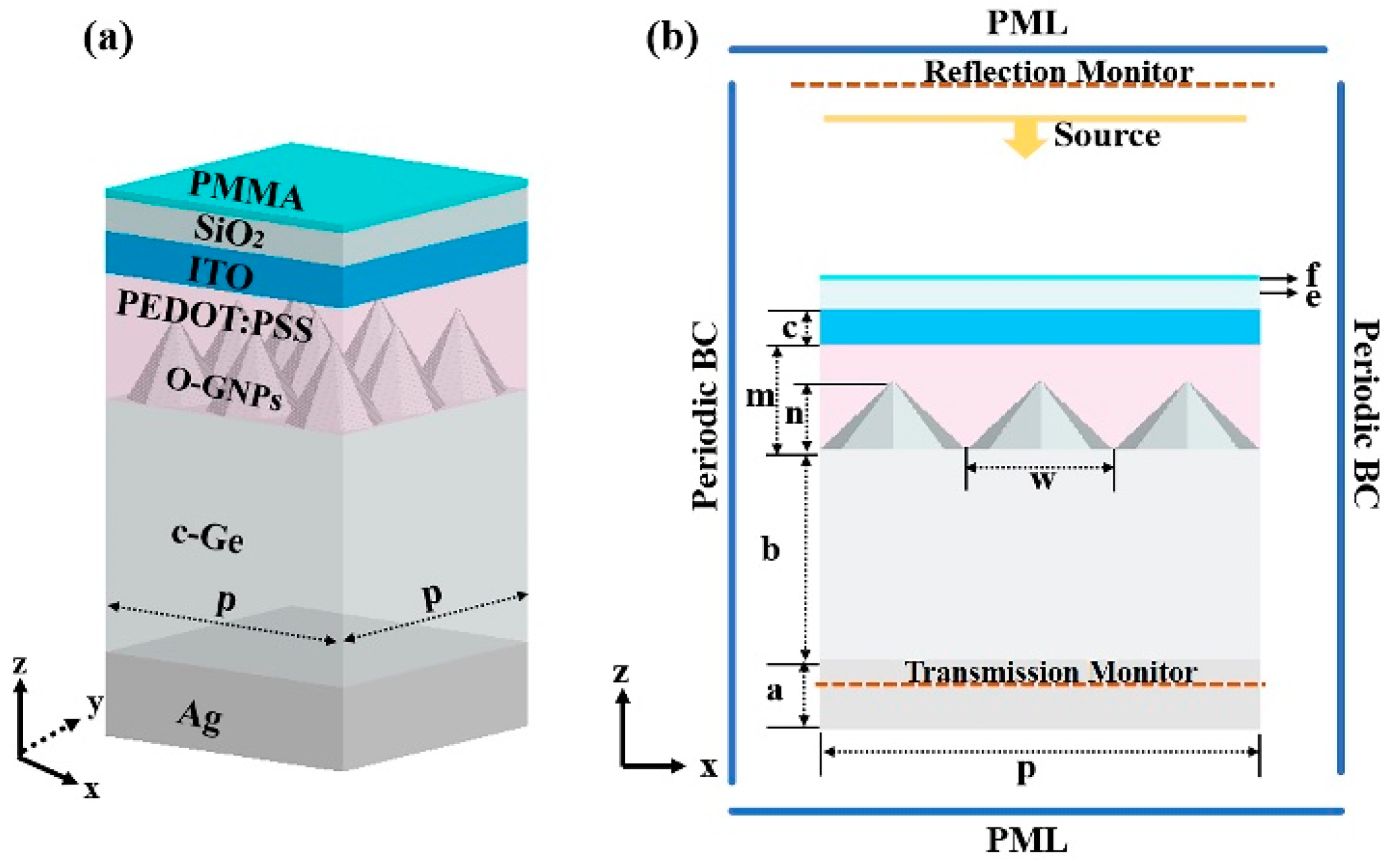
2. Design and Structures

2.1. Simulation Methods

The finite-difference time-domain (FDTD) solution is used for the optical emulation of solar cells. The FDTD method, proposed by KaneYee, refers to solving Maxwell’s equations in the time domain [42,43]. FDTD discretizes the differential equation by using the coupled Maxwell curl equation, divides the grid uniformly, and solves a series of sampled alternately electric and magnetic fields [44,45]. Moreover, FDTD can carry out wideband signal analysis, and, as long as the simulation of a pulse input, you can get very wide bandwidth information. Theoretically, the solution space is infinite. In the specific calculation, the perfect matching layer (PML) is adopted to carry out the special treatment in the finite space [46], so that there is no obvious reflection phenomenon in the boundary and no distortion in the field generated by the internal space. When FDTD is used, the light source is used as excitation. The light source is placed directly above the material, and the numerical wave generated by the light source eventually propagates to the structure, with a part transmitted and partially reflected. FDTD can calculate the generation rate of light [47], and its expression is [48]
G ( r ) = P abs ( r , ω ) ω = 0.5 | E ( r , ω ) | 2 I m [ ε ( r , ω ) ]
where Pabs is the absorption spatial power density, and its expression is [48]
P abs ( r , ω ) = 0.5 | E ( r , ω ) | 2 I m [ ε ( r , ω ) ]
ω refers to the angular frequency; E refers to the strength of the electric field; ε refers to dielectric constant; ℏω refers to the energy of a photon.
DEVICE was used for electrical stimulation. It is a tool to simulate electronic collection efficiency, and its essence is to calculate a series of Poisson equations and diffusion equations in a finite element grid [49]. In the calculation, the optical generation rate G( r ) after FDTD is imported; the semiconductor material is doped with N-type and P-type, and the base and emitter are added together to generate the motion of charge, and the motion of the carrier is calculated to obtain the parameter characteristics of the solar cell [50]. Short-circuit current [51], open-circuit voltage, conversion efficiency and the filling factor of solar cells are calculated by DEVICE software. The short-circuit current is the current value flowing through the two ends of the solar cell when the output end is a short circuit, and its expression is
  J SC = e c 200 nm 1500 nm Q E ( λ ) λ I AM 1 . 5 ( λ ) d λ    
where ℏ gets at a reduced Plank’s constant; c gets at speed of light in free space; QE gets at the Quantum Efficiency of Solar Cell [52].
Open-circuit voltage refers to the output voltage value of the solar cell when both ends are open-circuit, and its expression is [53]
  V oc = n k B T q In ( J sc J 0 + 1 )
where q is the charge amount of the electron; kB is boltzmann constant; T is temperature; Jsc is the short-circuit current, and J0 is dark current. We know from the expression that Voc has a direct relationship with Jsc when the temperature is constant. The filling factor (FF) is a significant index to measure the output capability of solar cells. The larger the value is, the greater the energy usage ratio, and then the quality of the cells is high, and so its expression is [54]
F F = P max V oc   ×   J sc
where Pmax is the maximum output power of a solar cell and the maximum product of the output current and output voltage. The conversion efficiency of a solar cell is equal to the ratio of the output power of the solar cell to the energy incident on the solar cell surface. It depends on the light intensity, also on the current and voltage of the cell material. Its expression is [54]
η = F F × V oc × J sc S AM 1 . 5
where SAM1.5 is the optical power incident on the unit area under the spectral condition of AM1.5, namely SAM1.5 = 100 mW/cm2. FF, Voc and Jsc have been defined above. Since DEVICE software is unable to compute the charge transport of the organic polymeric layer materials, the proposed DEVICE structure does not contain an organic layer [39].

2.2. Structure Design
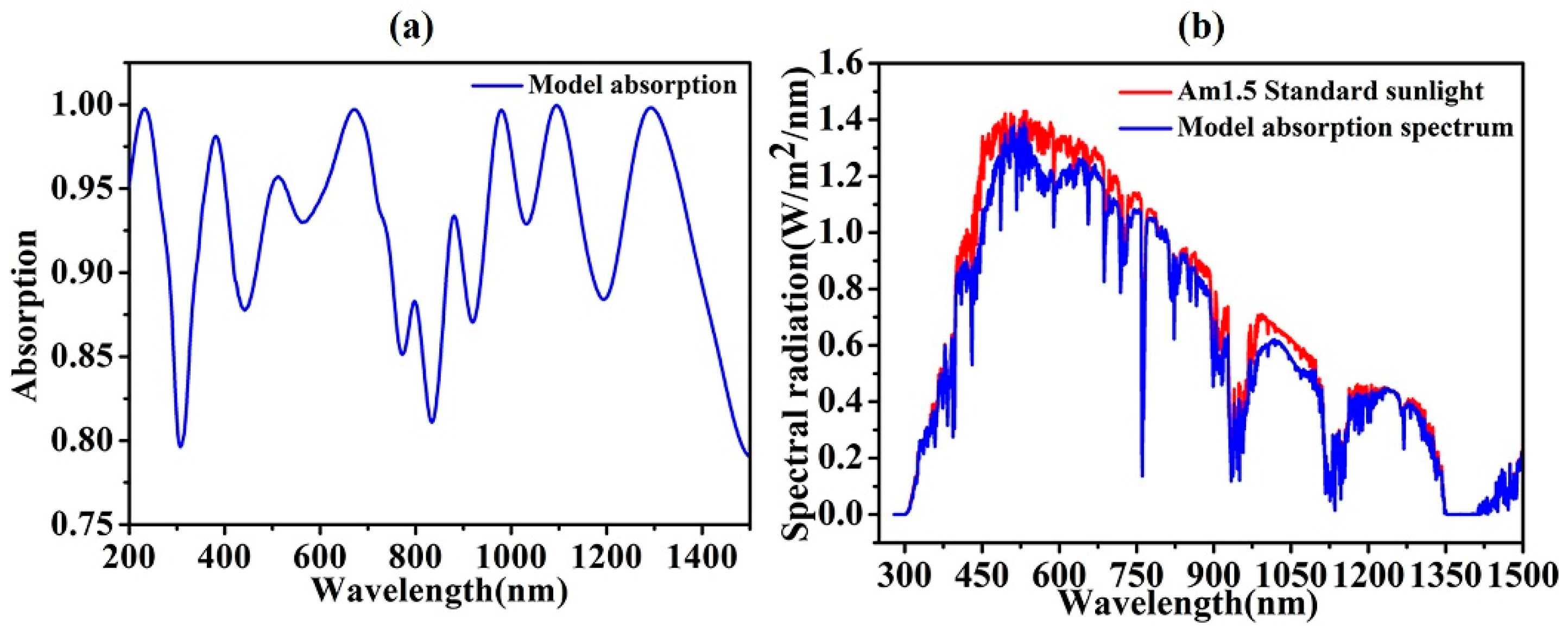
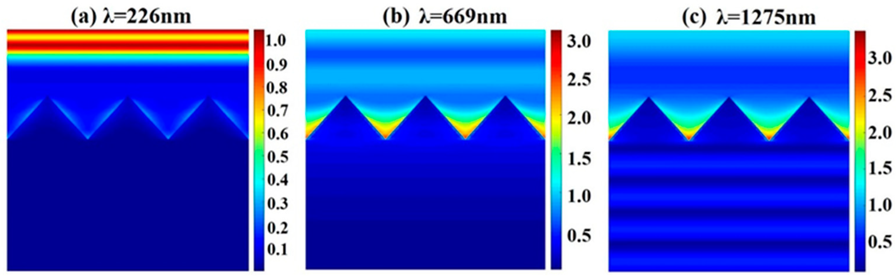
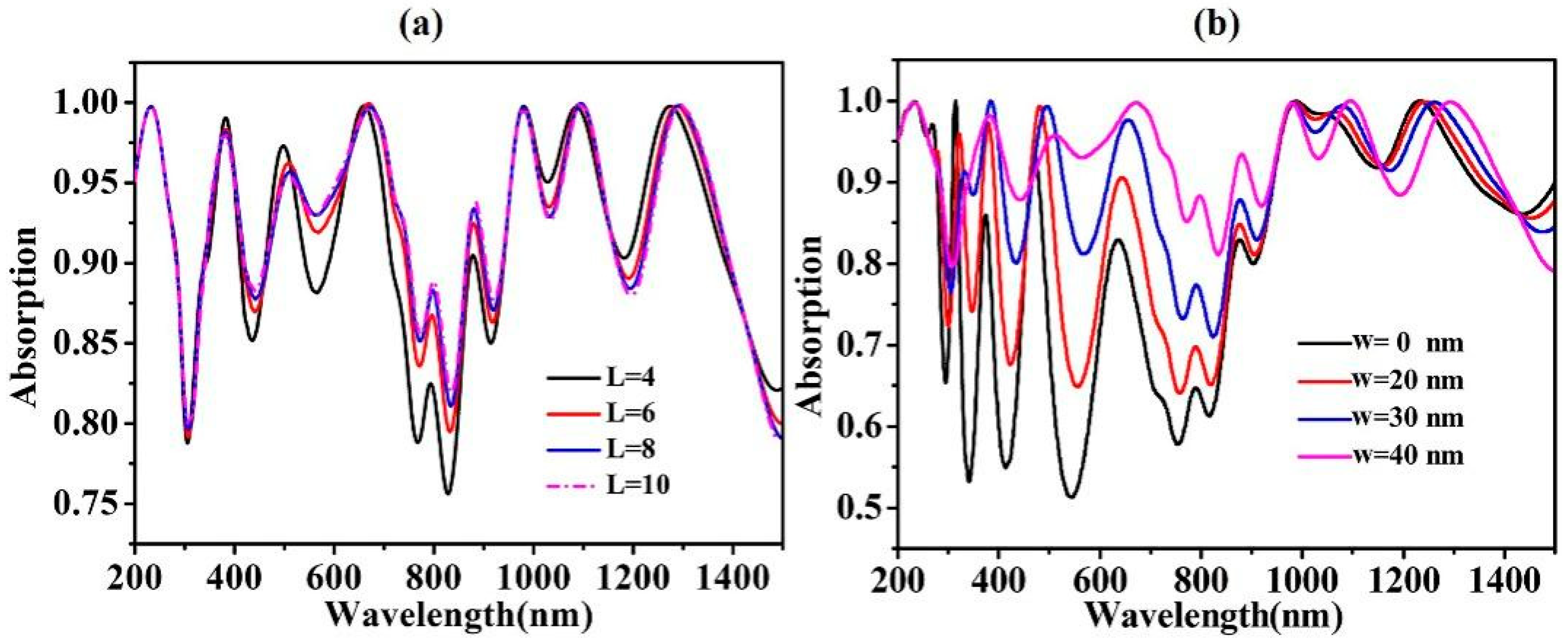
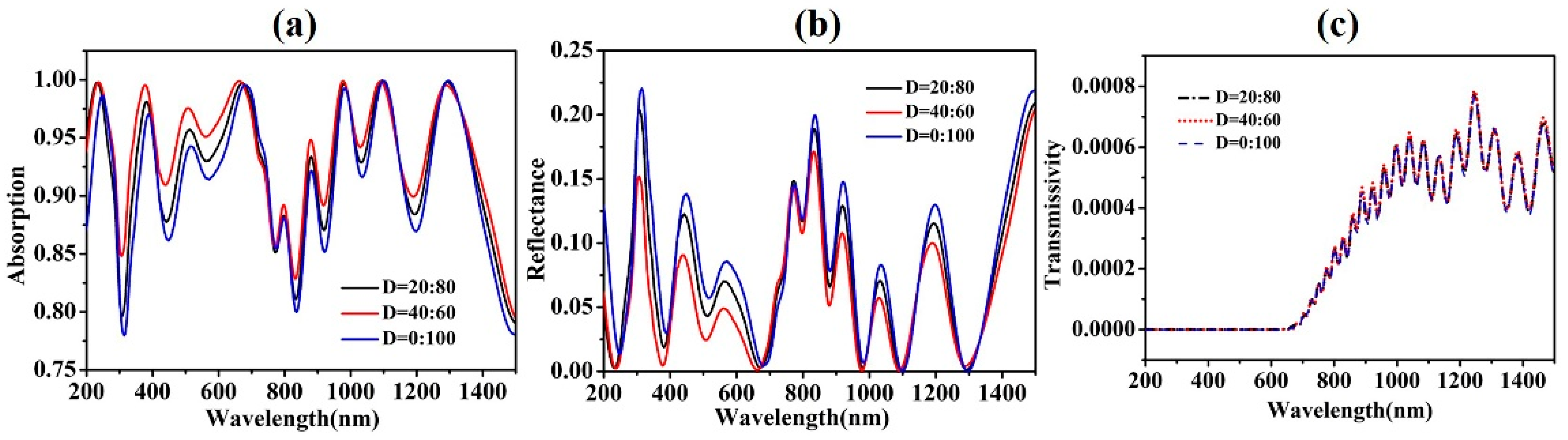
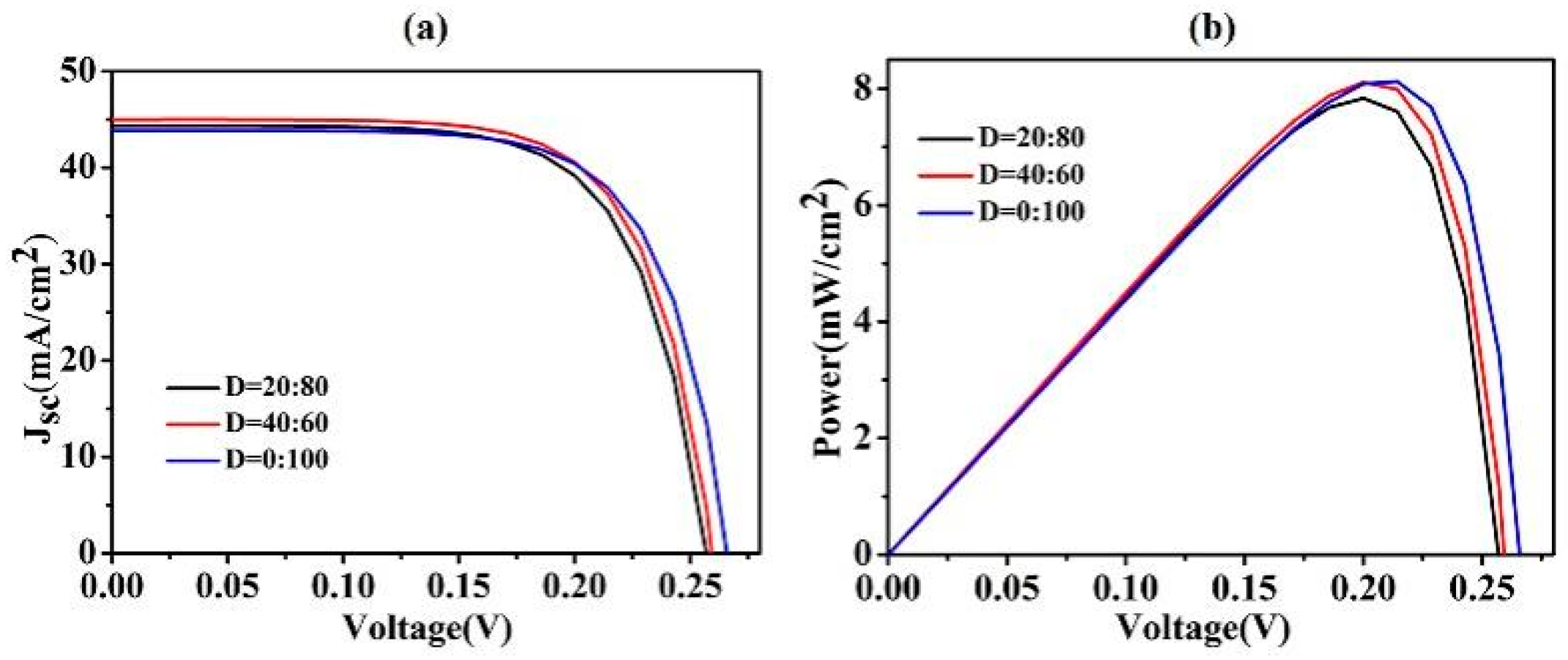
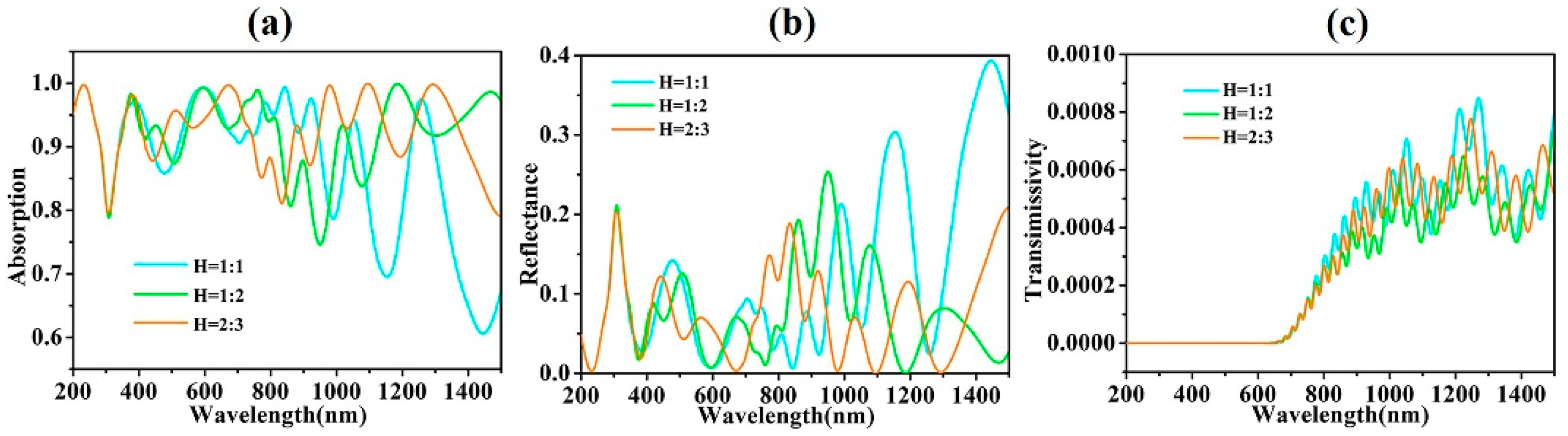
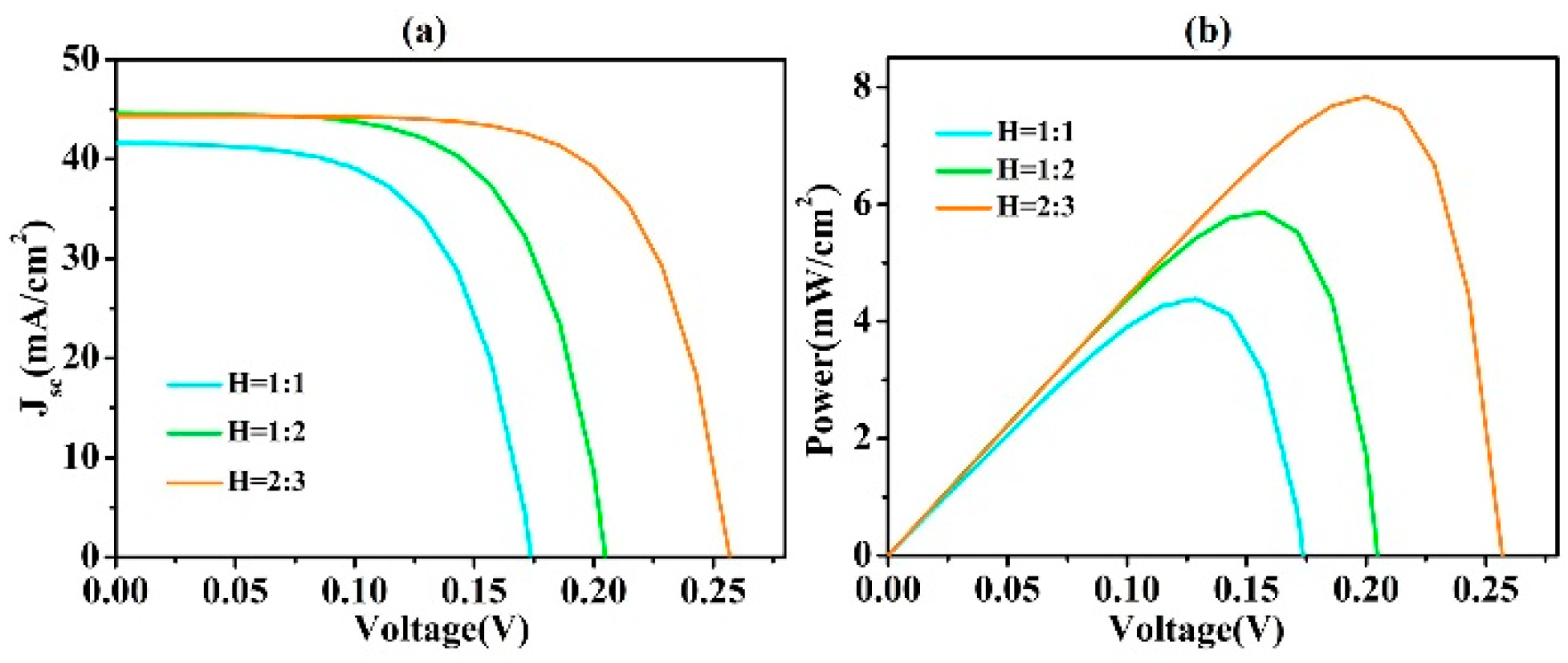
An organic active layer of PEDOT:PSS with O-GNPs on the backplate of Ag and the base of Ge was proposed; ITO was added, and the structure of the top layer combined with organic glass and SiO2 is shown in the three-dimensional diagram of Figure 1a. Its two-dimensional section is shown in Figure 1b. Then, p is the period of the entire structure, where p = 120 nm. The Ag layer is 200 nm thick, and the Ge layer is 600 nm thick. O-GNPs with a height of 200 nm were placed in the middle of the organic active layer to enhance absorption. The thickness of the ITO placed above PEDOT:PSS was 100 nm, which was used to increase the mobility of carriers [38]. The top layer is made of 80 nm SiO2 and 20 nm PMMA. PMMA is placed on the top layer due to its extremely high light transmittance. The edges of the whole structure x and y are the periodic boundary conditions used. PML is adopted at above and below of the z-axis. Directly above the material, the solar light source is used as the plane wave excitation source for simulation calculation. By placing two frequency-domain power monitors directly above the model at 1500 nm (Reflected power monitor) and at 160 nm (Transmitted power monitor) on the Ag layer, the reflectivity R and transmittance T can be calculated. The location of the transmission monitor was chosen because when the Ag layer is thick enough (greater than 100 nm), the effect of transmission can be ignored [55]. According to A = 1-R-T, the absorption rate of the structure can be obtained. By setting and analyzing the photon generation rate, the light generation rate of its solar cell can be obtained. The electric field distribution of the structure can be calculated by setting an electric field monitor.
The internal interference of the absorptive optical resonator composed of the cell’s semi-reflective front electrode and the highly reflective post-reflective layer can be enhanced by absorption [15]. So, we added to the DEVICE a blocky Al emitter with an ohmic contact on the front, and an Ag base covering the entire back surface with an ohmic contact on the back. The metal as the cathode of the device can collect electrons from the active layer. Metal electrodes on the surface of the organic layer not only diffuse into the polymer film but also interact strongly with the polymer material [56]. In addition, the interface properties between metal electrodes and polymers also have a significant impact on the exciton separation, transmission, collection and recombination processes in polymer solar cells, and ultimately affect the energy conversion efficiency and stability of HSCs. Because of the forbidden bandwidth of Ge, Eg = 0.66 eV. Only when the energy is greater than the bandgap width Eg, the photon will contribute energy Eg to the battery output, while the photon with the energy less than the bandgap width Eg will not contribute to the battery output, and the energy less than Eg will be consumed in the form of heat. After doping of the Ge material, the parameters of the cell such as current and voltage can be obtained.
Ge et al., who created the pyramid through single-point diamond turning (SPDT), said it could also be used to create more complex, high-quality three-dimensional structures [57]. Therefore, we used SPDT, nano-imprint lithography (NIL) and inductively-coupled plasma (ICP) etching to transfer the octagon pyramid structure from the copper mold to the doped germanium substrate to produce O-GNPs. Then, a layer of 200 nm Ag was deposited on the backplate of the Ge substrate by magnetron sputtering. The upper material is prepared from top to bottom. PMMA and SiO2 glass were bonded with Ethylene-vinyl acetate copolymer (EVA) adhesive, and a layer of ITO film was deposited on the glass sheet by magnetron sputtering, and then a layer of PEDOT:PSS was spun on the ITO film. A Ge substrate with nanoparticles was immersed in ITO/PEDOT:PSS, uising light to etch an electrode Al on the surface of the solar cell. Thus, the solar cell is completed.

3. Results

The model established in this paper has a good absorption efficiency, as shown in Figure 2a. Within the wavelength variation tendency of 200 to 1500 nm, the absorption rate of the solar cell is above 90% in most cases, and there are seven absorption peaks as high as 95%, which reflect the good absorption performance of the structure of the model. In Figure 2b, it can be seen that the solar cell’s ability to absorb sunlight is close to the standard spectrum AM1.5, with little loss of light, which again confirms the high absorption rate of the solar cell. We also calculate the electric field intensity at wavelengths λ = 226 nm, λ = 669 nm and λ = 1275 nm, where absorption is almost 100%, and plot its electric field intensity graph, as shown in Figure 3. Obviously, with the increase of wavelength, the electric field intensity increases gradually from (a) to (c), and the electric field near the O-GNPs increases significantly due to their unique light-trapping ability.
In Figure 3a, the high electric field at the top of O-GNPs leads to the enhancement of the generation of high-optical absorption coupled electron hole pairs, thus exhibiting high absorption characteristics. For mid-wavelength λ = 669 nm, the high electric field spreads along the sidewalls of the O-GNPs with high intensity; the constructive and destructive interference between the incoming and reflected wavelengths results in a diffraction distribution of the E-field distribution, as shown in Figure 3b. The electric field diffuses with a small intensity along the length of the Ge substrate. For the longer wavelength λ = 1275 nm, the incident photon reaches the back side of the HSCs, thus obtaining a more obvious diffraction distribution and improving the absorption spectrum at higher wavelengths in Figure 3c. From Figure 3a–c, it can be found that the electric field intensity around O-GNPs is increasing, and the number of photons absorbed by O-GNPs will increase with the increase of wavelength, which plays the role of light trapping [58,59]. We also studied the influence of the parameters of the form construction of Ge nanoparticles on light absorption. Suppose the edge number of the pyramid is L, and the absorption rate of solar cells varies according to different L.
In Figure 4a, it can be seen that at λ = 566 nm, λ = 760 nm and λ = 828 nm, the absorption increases with increasing the number of edges L. However, when L increases to 8, the effect of L on light absorption no longer changes significantly. When L = 10, its absorption rate is almost close to that of L = 8. Therefore, we propose ocpyramidal germanium nanoparticles (O-GNPs). In Figure 4b, w represents the width of an O-GNP. Obviously, with the increase in w, the absorbency effect of the solar cell on light is distinctly reinforced. When w increases to the maximum (three germanium nanoparticles just occupy the whole period p, then w = 40 nm), its absorption is the greatest. This is the trapping light enhancement of the O-GNPs. At the same time, we also studied the effect of the height n of the O-GNPs on the solar cell, as shown in Figure 5. When n increases from 160 to 220 nm, it can be seen from Figure 5a that the height change of O-GNPs has no obvious effect on photon absorption. However, as shown in Figure 5b, when n = 160 and 180 nm, the open-circuit voltage is far lower than that of n = 200 nm and n = 220 nm, indicating that the height of O-GNPs affects open-circuit voltage. When n = 200 nm, its short-circuit current reaches its highest value, which is 44.32 mA/cm2. In addition, the power voltage diagram in Figure 5c shows that when n = 200 nm, its maximum power is significantly higher than that of n = 160 nm and n = 180 nm, slightly higher than that of n = 220 nm. In summary, the specific parameters of germanium nanoparticles proposed by us are as follows: the octagonal conical germanium nanoparticles with a width of w = 40 nm, the height of n = 200 nm, the number of edges of L = 8 (O-GNPs).
Polymethyl methacrylate (PMMA), also known as plexiglass, is a synthetic polymer of methyl methacrylate. The material has good transparency and its transmittance is up to 92%. It can increase electron charge transmission and reduce defects [60,61], improve short-circuit current, open-circuit voltage and FF [62,63,64]. Therefore, PMMA was placed on the top layer as the light absorption layer in this paper, and we studied the solar cell absorption under different proportions of pervious glass and silica glass on the top layer of the structure, as shown in Figure 6. D is the ratio of PMMA to SiO2. Then, the absorption rate (A), reflectivity (R) and transmittance (T) of solar cells in different proportions are calculated. As can be seen from Figure 6, when it is all SiO2 (as shown in the solid blue line), it has the lowest absorption rate and the highest reflectivity. This is because the absorption rate of SiO2 is lower than that of PMMA, which is less effective in absorbing sunlight. So, we proposed a way to combine the two materials. When D reached 40:60, we found that the absorption rate was slightly higher than that of 20 nm PMMA. However, because PMMA is more expensive than ordinary glass, D = 20:80 is selected in this paper. It has a good absorption rate at the wavelength of 200 nm to 1500 nm, and the absorption rate is above 90% at most wavelengths. It follows that in Figure 6c that the transmittance difference between PMMA and SiO2 is not significant, indicating that the luminous flux through PMMA is equivalent to that of SiO2. We also used DEVICE simulation software to calculate its short-circuit current, open-circuit voltage curve and power voltage diagram, as shown in Figure 7. We can intuitively know from the figure that their short-circuit current is above 40 mA/cm2, and their open-circuit voltage is above 0.25 V, which indicates that the characteristics of the solar cells have been improved. As can be seen from the power voltage diagram, when all SiO2, is its open-circuit voltage and power maximum. This is because PMMA is an organic material, so in the calculation of electrical performance, PMMA is not added in the DEVICE simulation structure, resulting in that the PMMA charge transmission role is not reflected. As a result, when D = 20:80, its JSC and VOC are not much different from the other two cases but still relatively high.
At the same time, we also studied the effect of the O-GNPs and the thickness ratio H of the organic active layer PEDOT:PSS on the light absorption, as shown in Figure 8. In Figure 8a, the addition of the organic layer results in a good improvement in light absorption. In the short-wave range, a different H has little effect on the light absorption efficiency, but when the wavelength range is larger than 1000 nm, the absorption rate varies greatly: When H = 2:3, the absorption rate remains above 90%, which is the result of the interaction between the O-GNPs and the organic layer. It is obvious from Figure 8b,c that when H = 1:1, its reflectivity changes the most, because the thickness of the active layer is too thin, which does not play a good role in trapping light. When H is equal to 2:3, the reflectivity is much less than the other two, and the transmittance is in the middle, but because the transmittance values are very small, according to A = 1-R-T, when H = 2:3, it absorbs the photons best. So when H = 2:3, O-GNPs and the organic active layer structure are used. From the analysis of electrical performance, as shown in Figure 9a, as the thickness of the active layer increases, its short-circuit current and open-circuit voltage increase significantly, and its maximum power also increases, as shown in Figure 9b. When H = 2:3, its open-circuit voltage and power reach the maximum of 0.26 V and 7.84 mW/cm2, which are far more than the other two proportional structures. This is because the binding energy of a certain proportion of the organic active layer and O-GNPs greatly increases the mobility of carriers and promotes the motion of charges. Specific parameters such as its short-circuit current, maximum power and energy conversion efficiency are calculated in Table 1.

4. Conclusions

To sum up, we succeeded in analyzing the eight pyramid-type optical properties of the nanometer particle structure, which is based on eight pyramid-type Ge nanoparticles of PEDOT: PSS/c-Ge HSCs from light absorption and electric field intensity, short-circuit current, open-circuit voltage and energy conversion efficiency, resulting in the short-circuit current Jsc of 44.32 mA/cm2, open-circuit voltage VOC of 0.26 V and the energy conversion efficiency of 7.84% high-performance heterojunction solar cells. The addition of PMMA can better absorb photons and improve the absorption rate of light, which provides new research for solar cells. In this paper, the proposed ocpyramid-shaped nanoparticles increase the diversity of single spherical nanoparticles, which provides a deeper understanding of the application of nanoparticles in solar cells.

Author Contributions

Conceptualization, J.S., H.Y., and Z.Y.; data curation, Z.Y., Y.X. and H.Y.; formal analysis, F.Z. (Fei Zhao) and L.L.; methodology, J.S., H.Y., Y.X., Y.T., Z.Y. and H.L.; resources, H.L.; software, Y.X., Y.T., Z.Y., F.Z. (Fusheng Zheng) and P.W.; data curation, J.S.; writing-original draft preparation, J.S.; writing-review and editing, H.Y., H.L., L.L. and H.L. All authors have read and agreed to the published version of the manuscript.

Funding

The authors are grateful to the support by National Natural Science Foundation of China (No. 51606158, 11604311, 61705204, 21506257); the Funded by the Scientific Research Fund of Si Chuan Provincial Science and Technology Department (2020YJ0137; 2020YFG0467; 2021JDRC0019); the Funded by the Open Fund of The Key Laboratory for Metallurgical Equipment and Control Technology of Ministry of Education in Wuhan University of Science and Technology (No. MECOF2020B02); the Funded by the Undergraduate Innovation Fund Project Precision Funding by Southwest University of Science and Technology (No. JZ20–025); the Postgraduate Innovation Fund Project by Southwest University of Science and Technology (No. 18ycx034); the Funded by Southwest University of Science and Technology Students Innovation Fund project (No. CX20–031).

Institutional Review Board Statement

Not applicable.

Informed Consent Statement

Not applicable.

Data Availability Statement

Publicly available datasets were analyzed in this study. This data can be found here: [https://www.lumerical.com/].

Conflicts of Interest

The authors declare no conflict of interest.

References

  1. Yi, Z.; Li, J.K.; Lin, J.C.; Qin, F.; Chen, X.F.; Yao, W.T.; Liu, Z.M.; Cheng, S.B.; Wu, P.H.; Li, H.L. Broadband polariza-tion-insensitive and wide-angle solar energy absorber based on tungsten ring-disc array. Nanoscale 2020, 12, 23077–23083. [Google Scholar] [CrossRef] [PubMed]
  2. Li, J.; Chen, X.; Yi, Z.; Yang, H.; Tang, Y.; Yi, Y.; Yao, W.; Wang, J.; Yi, Y. Broadband solar energy absorber based on monolayer molybdenum disulfide using tungsten elliptical arrays. Mater. Today Energy 2020, 16, 100390. [Google Scholar] [CrossRef]
  3. Chen, X.; Wu, W.; Zhang, W.; Wang, Z.; Fu, Z.; Zhou, L.; Yi, Z.; Li, G.; Zeng, L. Blue and green double band luminescent carbon quantum dots: Synthesis, origin of photoluminescence, and application in white light-emitting devices. Appl. Phys. Lett. 2021, 15, 153102. [Google Scholar] [CrossRef]
  4. Deng, Y.; Cao, G.T.; Yang, H.; Zhou, X.Q.; Wu, Y.W. Dynamic control of double plasmon-induced transparencies in aperture-coupled waveguide-cavity system. Plasmonics 2018, 13, 345–352. [Google Scholar] [CrossRef]
  5. Liu, W.; Pang, L.; Han, H.; Bi, K.; Lei, M.; Wei, Z. Tungsten disulphide for ultrashort pulse generation in all-fiber lasers. Nanoscale 2017, 9, 5806–5811. [Google Scholar] [CrossRef] [PubMed]
  6. Cheng, Z.H.; Liao, J.; He, B.Z.; Zhang, F.; Zhang, F.A.; Huang, X.H.; Zhou, L. One-step fabrication of graphene oxide enhanced magnetic composite gel for highly efficient dye adsorption and catalysis. ACS Sustain. Chem. Eng. 2015, 3, 1677–1685. [Google Scholar] [CrossRef]
  7. Cheng, T.; Sun, X.; Xian, T.; Yi, Z.; Li, R.; Wang, X.; Yang, H. Tert-butylamine/oleic acid-assisted morphology tailoring of hierarchical Bi4Ti3O12 architectures and their application for photodegradation of simulated dye wastewater. Opt. Mater. 2021, 112, 110781. [Google Scholar] [CrossRef]
  8. Li, J.H.; Jiang, J.B.; Xu, Z.F.; Liu, M.Q.; Tang, S.P.; Yang, C.M.; Qian, D. Facile synthesis of Ag@Cu2O heterogeneous nanocrystals decorated N-doped reduced graphene oxide with enhanced electrocatalytic activity for ultrasensitive detection of H2O2. Sens. Actuators B Chem. 2018, 260, 529–540. [Google Scholar] [CrossRef]
  9. King, R.R.; Law, D.C.; Edmondson, K.M.; Fetzer, C.M.; Kinsey, G.S. 40% efficient metamorphic GaInP/GaInAs/Ge multijunction solar cells. Appl. Phys. Lett. 2007, 90, 183516. [Google Scholar] [CrossRef] [Green Version]
  10. Bunthof, L.A.A.; Haverkamp, E.J.; Woude, D.V.; Bauhuis, G.J.; Corbeek, W.H.M.; Veelenturf, S.; Vlieg, E.; Schermer, J.J. Influence of laterally split spectral illumination on multi-junction CPV solar cell performance. Sol. Energy 2018, 170, 86–94. [Google Scholar] [CrossRef]
  11. Renno, C.; Landi, G.; Petito, F.; Neitzert, H.C. Influence of a degraded triple-junction solar cell on the CPV system performances. Energy Convers. Manag. 2018, 160, 326–340. [Google Scholar] [CrossRef]
  12. Zhou, Q.; Ju, W.; Yong, Y.; Zhang, Q.; Liu, Y.; Li, J. Effect of the N/P and transition-metal co-doping on the quantum capacitance of supercapacitor electrodes based on mono-and multilayer graphene. Carbon 2020, 170, 368–379. [Google Scholar] [CrossRef]
  13. Huen, P.; Daoud, W.A. Advances in hybrid solar photovoltaic and thermoelectric generators. Renew. Sustain. Energy Rev. 2017, 72, 1295–1302. [Google Scholar] [CrossRef]
  14. Ahmed, A.; Zhang, G.; Shanks, K.; Sundaram, S.; Ding, Y.L.; Mallick, T. Performance evaluation of single multi-junction solar cell for high concentrator photovoltaics using minichannel heat sink with nanofluids. Appl. Therm. Eng. 2021, 182, 115868. [Google Scholar] [CrossRef]
  15. Lattyak, C.; Ravekes, R.E.; Steenhoff, V.; Vehse, M.; Agert, C. Ultrathin resonant-cavity-enhanced amorphous germanium solar cells on ZnO. IEEE J. Photovolt. 2018, 8, 3–7. [Google Scholar] [CrossRef]
  16. Hekmatshoar, B.; Shahrjerdi, D.; Hopstaken, M.; Fogel, K.; Sadana, D.K. High-efficiency heterojunction solar cells on crystalline germanium substrates, oxide-based materials & devices v, international society for optics and photonics. Appl. Phys. Lett. 2012, 101, 032102. [Google Scholar]
  17. Barrutia, L.; Garcia, I.; Barrigon, E.; Ochoa, M.; Algora, C.; Solle, I.R. Impact of the III-V/Ge nucleation routine on the performance of high efficiency multijunction solar cells. Sol. Energy Mater. Sol. Cells 2020, 207, 110355. [Google Scholar] [CrossRef]
  18. Qi, Y.; Zhang, B.; Ding, J.; Zhang, T.; Wang, X.; Yi, Z. Efficient manipulation of terahertz waves by multi-bit coding metasurfaces and its further application. Chin. Phys. B 2020, 30, 024211. [Google Scholar] [CrossRef]
  19. Liu, Q.; Khatri, I.; Ishikawa, R.; Ueno, K.; Shirai, H. Effects of molybdenum oxide molecular doping on the chemical structure of poly(3,4-ethylenedioxythiophene):poly(stylenesulfonate) and on carrier collection efficiency of silicon/poly(3,4-ethylenedioxythiophene):poly(stylenesulfonate) heterojunction solar cells. Phys. Lett. 2013, 102, 183503. [Google Scholar]
  20. Roghabadi, F.A.; Ahmadi, N.; Ahmadi, V.; Carlo, A.D.; Aghmiuni, K.O.; Tehrani, A.S.; Ghoreishi, F.S.; Payandeh, M.; Fumani, N.M.R. Bulk heterojunction polymer solar cell and perovskite solar cell: Concepts, materials, current status, and opto-electronic properties. Sol. Energy 2018, 173, 407–424. [Google Scholar] [CrossRef]
  21. Li, P.C.; Sun, K.; Ouyang, J.Y. Stretchable and conductive polymer films prepared by solution blending. Appl. Mater. Interfaces 2015, 7, 18415–18423. [Google Scholar] [CrossRef] [PubMed]
  22. Yi, M.J.; Jang, W.; Cho, J.S.; Wang, D.H. Enhanced interface of polyurethane acrylate via perfluoropolyether for efficient transfer printing and stable operation of PEDOT:PSS in perovskite photovoltaic cells. Appl. Surf. Sci. 2019, 467–468, 168–177. [Google Scholar] [CrossRef]
  23. Li, Z.; Yi, Y.; Xu, D.; Yang, H.; Yi, Z.; Chen, X.; Yi, Y.; Zhang, J.; Wu, P. A multi-band and polarization-independent perfect absorber based on dirac semimetals circles and semi-ellipses array. Chin. Phys. B 2021. [Google Scholar] [CrossRef]
  24. Zhang, X.; Liu, Z.; Zhang, Z.; Gao, E.; Luo, X.; Zhou, F.; Li, H.; Yi, Z. Polarization-sensitive triple plasmon-induced transparency with synchronous and asynchronous switching based on monolayer graphene metamaterials. Opt. Express 2020, 28, 36771–36783. [Google Scholar] [CrossRef] [PubMed]
  25. Zhang, B.; Qi, Y.; Zhang, T.; Zhang, Y.; Liu, W.; Wang, L.; Ding, J.; Wang, X.; Yi, Z. Tunable multi-band terahertz absorber based on composite graphene structures with square ring and Jerusalem cross. Results Phys. 2021, 25, 104233. [Google Scholar] [CrossRef]
  26. Lee, J.H.; Kim, Y.H. High performance ITO-free white organic light-emitting diodes using highlyconductive PEDOT:PSS transparent electrodes. Synth. Met. 2018, 242, 99–102. [Google Scholar] [CrossRef]
  27. Gogolin, R.; Zielke, D.; Descoeudres, A.; Despeisse, M.; Ballif, C.; Schmdt, J. Demonstrating the high voc potential of PEDOT:PSS/c-Si heterojunctions on solar cells. Energy Procedia 2017, 124, 593–597. [Google Scholar] [CrossRef] [Green Version]
  28. Minemoto, T.; Kawano, Y.; Nishimura, T.; Shen, Q.; Yoshino, K.; Likubo, S.; Hayase, S.; Chantana, J. Theoretical analysis of band alignment at back junction in Sn–Ge perovskite solar cells with inverted p-i-n structure. Sol. Energy Mater. Sol. Cells 2020, 206, 110268. [Google Scholar] [CrossRef]
  29. Zhao, F.; Chen, X.F.; Yi, Z.; Qin, F.; Tang, Y.J.; Yao, W.T.; Zhou, Z.G.; Yi, Y.G. Study on the solar energy absorption of hybrid solar cells with trapezoid-pyramidal structure based PEDOT:PSS/c-Ge. Solar Energy 2020, 204, 635–643. [Google Scholar] [CrossRef]
  30. Li, J.H.; Jiang, J.B.; Zhao, D.; Xu, Z.F.; Liu, M.Q.; Liu, X.; Tong, H.X.; Qian, D. Novel hierarchical sea urchin-like Prussian blue@palladium core-shell heterostructures supported on nitrogen-doped reduced graphene oxide: Facile synthesis and excellent guanine sensing performance. Electrochim. Acta 2020, 330, 135196. [Google Scholar] [CrossRef]
  31. Yang, X.; Zhang, F.; Hu, Y.J.; Chen, D.Z.; He, Z.Q.; Xiong, L.Z. Gold nanoparticals doping graphene sheets nanocomposites sensitized screen-printed carbon electrode as a disposable platform for voltammetric determination of guaiacol in bamboo juice. Int. J. Electrochem. Sci. 2014, 9, 5061–5072. [Google Scholar]
  32. Lu, W.H.; Wang, C.W.; Yue, W.; Chen, L.W. Si/PEDOT:PSS core/shell nanowire arrays for efficient hybrid solar cells. Nanoscale 2011, 3, 3631. [Google Scholar] [CrossRef] [PubMed]
  33. Mariani, G.; Wang, Y.; Wong, P.S.; Lech, A.; Hung, C.H.; Shapiro, J.; Prikhodko, S.; El-Kady, M.; Kaner, R.B.; Huffaker, D.L. Three-dimensional core−shell hybrid solar cells via controlled in situ materials engineering. Nano Lett. 2012, 12, 3581–3586. [Google Scholar] [CrossRef]
  34. Han, S.E.; Chen, G. Optical absorption enhancement in silicon nanohole arrays for solar photovoltaics. Nano Lett. 2010, 10, 1012–1015. [Google Scholar] [CrossRef] [PubMed]
  35. Garnett, E.; Yang, P.D. Light trapping in silicon nanowire solar cells. Nano Lett. 2010, 10, 1082–1087. [Google Scholar] [CrossRef] [PubMed]
  36. Ren, R.; Zhong, Z. Enhanced light absorption of silicon solar cells with dielectric nanostructured back reflector. Opt. Commun. 2018, 417, 110–114. [Google Scholar] [CrossRef]
  37. Liu, B.; Hu, J.; Jia, L.J.; Liu, J.; Ren, X.D.; Zhang, X.S.; Guo, X.J.; Liu, S.Z. Ge quantum-dot enhanced c–Si solar cell for improved light trapping efficiency. Sol. Energy 2018, 167, 102–107. [Google Scholar] [CrossRef]
  38. Agnihotri, S.K.; Samajdar, D.P.; Arefinia, Z. Design of InP-based truncated nanopyramid solar cells with conformal coating of PEDOT: PSS for improved light harvesting efficiency. Opt. Mater. 2020, 110, 110475. [Google Scholar] [CrossRef]
  39. Sachchidanand, D.P.S. Light-trapping strategy for PEDOT:PSS/c-Si nanopyramid based hybrid solar cells embedded with metallic nanoparticles. Sol. Energy 2019, 190, 278–285. [Google Scholar] [CrossRef]
  40. Xue, D.J.; Wang, J.J.; Wang, Y.Q.; Xin, S.; Guo, Y.G.; Wan, L.J. Facile synthesis of germanium nanocrystals and their application in organic–inorganic hybrid photodetectors. Adv. Mater. 2011, 23, 3704–3707. [Google Scholar] [CrossRef]
  41. Amollo, T.A.; Mola, G.T.; Nyamori, V.O. Improved short-circuit current density in bulk heterojunction solar cells with reduced graphene oxide-germanium dioxide nanocomposite in the photoactive layer. Mater. Chem. Phys. 2020, 254, 123448. [Google Scholar] [CrossRef]
  42. Chen, Z.; Chen, H.; Yin, J.; Zhang, R.; Jile, H.; Xu, D.; Yi, Z.; Zhou, Z.; Cai, S.; Yan, P. Multi-band, tunable, high figure of merit, high sensitivity single-layer patterned graphene—perfect absorber based on surface plasmon resonance. Diam. Relat. Mater. 2021, 116, 108393. [Google Scholar] [CrossRef]
  43. Chen, Z.; Chen, H.; Jile, H.; Xu, D.; Yi, Z.; Lei, Y.; Chen, X.; Zhou, Z.; Cai, S.; Li, G. Multi-band multi-tunable perfect plasmon absorber based on L-shaped and double-elliptical graphene stacks. Diam. Relat. Mater. 2021, 115, 108374. [Google Scholar] [CrossRef]
  44. Wang, Y.; Yi, Y.; Xu, D.; Yi, Z.; Li, Z.; Chen, X.; Jile, H.; Zhang, J.; Zeng, L.; Li, G. Terahertz tunable three band narrowband perfect absorber based on dirac semimetal. Phys. E Low-Dimens. Syst. Nanostruct. 2021, 131, 114750. [Google Scholar] [CrossRef]
  45. Zhang, Y.; Yi, Z.; Wang, X.; Chu, P.; Yao, W.; Zhou, Z.; Cheng, S.; Liu, Z.; Wu, P.; Pan, M.; et al. Dual band visible metamaterial absorbers based on four identical ring patches. Phys. E Low-Dimens. Syst. Nanostruct. 2021, 127, 114526. [Google Scholar] [CrossRef]
  46. Zhang, Z.H.; Cai, R.; Long, F.; Wang, J. Development and application of tetrabromobisphenol A imprinted electrochemical sensor based on graphene/carbon nanotubes three-dimensional nanocomposites modified carbon electrode. Talanta 2015, 134, 435–442. [Google Scholar] [CrossRef] [PubMed]
  47. Zhang, Z.; Liu, Z.; Zhou, F.; Wang, J.; Wang, Y.; Zhang, X.; Qin, Y.; Zhuo, S.; Luo, X.; Gao, E.; et al. Broadband plasmon-induced transparency modulator in the terahertz band based on multilayer graphene metamaterials. JOSA A 2021, 38, 784–789. [Google Scholar] [CrossRef] [PubMed]
  48. Zhang, X.; Liu, Z.; Zhang, Z.; Qin, Y.; Zhuo, S.; Luo, X.; Zhou, F.; Yi, Z.; Wang, J.; Wang, Y. Triple plasmon-induced transparency in graphene and metal metamaterials and its anomalous property. J. Phys. D Appl. Phys. 2021, 54, 284001. [Google Scholar] [CrossRef]
  49. Wang, Y.; Cui, W.; Ma, H.; Xu, H.; Yi, Z.; Cao, X.; Ren, X.; He, Z. Outstanding slow-light effect for graphene metasurface in terahertz. Results Phys. 2021, 23, 104002. [Google Scholar] [CrossRef]
  50. He, Z.; Li, L.; Cui, W.; Wang, Y.; Xue, W.; Xu, H.; Yi, Z.; Li, C.; Li, Z. Unidirectional reflectionless propagation of near-infrared light in resonator-assisted non-parity-time symmetric waveguides. New J. Phys. 2021, 23, 053015. [Google Scholar] [CrossRef]
  51. Liu, Z.; Zhang, X.; Zhou, F.; Luo, X.; Zhang, Z.; Qin, Y.; Zhuo, S.; Gao, E.; Li, H.; Yi, Z. Triple plasmon-induced transparency and optical switch desensitized to polarized light based on a mono-layer metamaterial. Opt. Express 2021, 29, 13949–13959. [Google Scholar] [CrossRef]
  52. Wang, X.X.; Zhu, J.K.; Xu, Y.Q.; Qi, Y.P.; Zhang, L.P.; Yang, H.; Yi, Z. A novel plasmonic refractive index sensor based on gold/silicon complementary grating structure. Chin. Phys. B 2021, 2, 024207. [Google Scholar] [CrossRef]
  53. Chang, K.F.; Chen, Y.C.; Chang, K.W.; Shellaiah, M.; Sun, K.W. Junction model and transport mechanism in hybrid PEDOT:PSS/n-GaAs solar cells. Org. Electron. 2017, 51, 435–441. [Google Scholar] [CrossRef]
  54. Han, G.; Zhang, S.; Boix, P.P.; Wong, L.H.; Sun, L.; Lien, S.Y. Towards high efficiency thin film solar cells. Prog. Mater. Sci. 2017, 87, 246–291. [Google Scholar] [CrossRef]
  55. Chen, L.; Wang, Q.K.; Shen, X.Q.; Chen, W.; Huang, K.; Liu, D.M. Absorption enhancement in thin film a-Si solar cells with double-sided SiO2 particle layers. Chin. Phys. B 2015, 24, 104201. [Google Scholar] [CrossRef]
  56. Nolasco, J.C.; Castro-Carranza, A.; León, Y.A.; Jurado, C.B.; Gutowski, J.; Parisi, J.; Hauff, E.V. Understanding the open circuit voltage in organic solar cells on the basis of a donor-acceptor abrupt (p-n++) heterojunction. Sol. Energy 2019, 184, 610–619. [Google Scholar] [CrossRef]
  57. Ge, S.B.; Liu, W.G.; Zhou, S.; Li, S.J.; Sun, X.P.; Huang, Y.T.; Yang, P.F.; Zhang, J.; Lin, D.B. design and preparation of a micro-pyramid structured thin film for broadband infrared antireflection. Coatings 2018, 8, 192. [Google Scholar] [CrossRef] [Green Version]
  58. Lin, X.; Li, Y.J.; Chen, F.T.; Xu, P.; Li, M. Facile synthesis of mesoporous titanium dioxide doped by Ag-coated graphene with enhanced visible-light photocatalytic performance for methylene blue degradation. RSC Adv. 2017, 7, 25314–25324. [Google Scholar]
  59. Long, F.; Zhang, Z.H.; Wang, J.; Yan, L.; Zhou, B.W. Cobalt-nickel bimetallic nanoparticles decorated graphene sensitized imprinted electrochemical sensor for determination of octylphenol. Electrochim. Acta 2015, 168, 337–345. [Google Scholar] [CrossRef]
  60. Yang, M.; Kong, Q.; Feng, W.; Yao, W. N/O double-doped biomass hard carbon material realizes fast and stable potassium ion storage. Carbon 2021, 176, 71–82. [Google Scholar] [CrossRef]
  61. Lv, P.P.; Xie, D.D.; Zhang, Z.H. Magnetic carbon dots based molecularly imprinted polymers for fluorescent detection of bovine hemoglobin. Talanta 2018, 188, 145–151. [Google Scholar] [CrossRef] [PubMed]
  62. Peng, J.; Khan, J.I.; Liu, W.; Ugur, E.; Duong, T.; Wu, Y.; Shen, H.; Wang, K.; Dang, H.; Aydin, E.; et al. A universal double-side passivation for high open-circuit voltage in perovskite solar cells: Role of carbonyl groups in poly(methyl methacrylate). Adv. Energy Mater. 2018, 8, 1801208. [Google Scholar] [CrossRef] [Green Version]
  63. Cai, L.; Zhang, Z.H.; Xiao, H.M.; Chen, S.; Fu, J.L. An eco-friendly imprinted polymer based on graphene quantum dots for fluorescent detection of p-nitroaniline. RSC Adv. 2019, 9, 41383–41391. [Google Scholar] [CrossRef] [Green Version]
  64. Ibrahim, M.L.I. The effect of injection barrier on the open-circuit voltage of organic photovoltaic cells. Mater. Today Proc. 2020, 29, 48–51. [Google Scholar] [CrossRef]
Figure 1. (a) Represents three-dimensional diagram of O-GNPs/PEDOT:PSS/ITO HSC in which the thickness of each layer of material has been plotted. (b) Represents a 2D diagram of the solar cell, and its simulation boundary conditions and monitor are presented.
Coatings 11 00748 g001
Figure 2. (a) The absorption changes at different wavelengths of the model. (b) The comparison of its absorption spectrum with the standard solar spectrum AM1.5 (the height of Ag: a = 200 nm; the height of Ge: b = 600 nm; the height of PEDOT:PSS: m = 300 nm; the height of Ge NP: n = 200 nm; the height of ITO: c = 100 nm; the height of SiO2: e = 80 nm; the height of PMMA: f = 20 nm).
Coatings 11 00748 g002
Figure 3. It is the electric field intensity diagram of the structure at λ = 226 nm (a), λ = 669 nm (b) and λ = 1275 nm (c).
Coatings 11 00748 g003
Figure 4. (a) The absorption of O-GNPs with different edge numbers at different wavelengths. (b) The absorption of O-GNPs with different width at different wavelengths.
Coatings 11 00748 g004
Figure 5. (a) The effect of the height of germanium nanoparticles on the light absorption of the solar cell. (b,c) Effects of the height of germanium nanoparticles on short-circuit current-open voltage curves and power-open voltage curves of solar cells. (L = 8, w = 40 nm).
Coatings 11 00748 g005
Figure 6. The influence of different transmittance materials thickness ratio D on (a) absorption, (b) reflectivity and (c) transmittance of the HSC. (L = 8, w = 40 nm, n = 200 nm).
Coatings 11 00748 g006
Figure 7. I-V curve (a) and P-V curve (b) under different thickness ratios of transmittance materials D.
Coatings 11 00748 g007
Figure 8. Different PEDOT:PSS and O-GNPs thickness ratio H have (a) absorption, (b) reflectivity and (c) transmittance of the model. (L = 8, w = 40 nm, n = 200 nm, D = 20:80).
Coatings 11 00748 g008
Figure 9. I-V curve (a) and P-V curve (b) under thickness ratio H of different PEDOT:PSS and O-GNPs.
Coatings 11 00748 g009
Table 1. The specific values were calculated by the software Lumerical DEVICE under thickness ratio H of different PEDOT:PSS and O-GNPs.
HVOC (V)JSC (mA/cm2)P (mW/cm2)FF (%)η (%)
1:10.1741.584.3961%4.38
1:20.2144.595.8764%5.87
2:30.2644.327.8469%7.84
Publisher’s Note: MDPI stays neutral with regard to jurisdictional claims in published maps and institutional affiliations.

