Article

A Tunable “Ancient Coin”-Type Perfect Absorber with High Refractive Index Sensitivity and Good Angular Polarization Tolerance

1
School of Science, Southwest University of Science and Technology, Mianyang 621010, China
2
School of Physics and Optoelectronic Engineering, Yangtze University, Jingzhou 434023, China
3
College of Physics and Electronics, Central South University, Changsha 410083, China
4
Basic Teaching Department, Neusoft Institute Guangdong, Foshan 528000, China
*
Authors to whom correspondence should be addressed.
These authors contribute equally to this article.
Coatings 2021, 11(7), 814; https://doi.org/10.3390/coatings11070814
Submission received: 14 May 2021 / Revised: 29 June 2021 / Accepted: 29 June 2021 / Published: 6 July 2021
(This article belongs to the Special Issue Micro-Nano Optics and Its Applications)

Abstract

:
In this paper, we design and present a graphene-based “ancient coin”-type dual-band perfect metamaterial absorber, which is composed of a silver layer, silicon dioxide layer, and a top “ancient coin” graphene layer. The absorption performance of the absorber is affected by the hollowed-out square in the center of the graphene layer and geometric parameters of the remaining nano disk. The optical properties of graphene can be changed by adjusting the voltage, to control the absorption performance of the absorber dynamically. In addition, the centrally symmetric pattern structure greatly eliminates the polarization angle dependence of our proposed absorber, and it exhibits good angular polarization tolerance. Furthermore, the proposed “ancient coin”-type absorber shows great application potential as a sensor or detector in biopharmaceutical, optical imaging, and other fields due to its strong tunability and high refractive index sensitivity.

1. Introduction

The concept of metamaterials (MMs) was first proposed by Rodger M. Walser in 2001 to describe an artificially designed composite material with a periodic unit structure [1]. The overall characteristics of metamaterials are determined by the characteristics of the periodic structure unit cell, which has little to do with the material itself [2,3,4]. The constitutive parameters of metamaterials, that is, the effective permittivity εeff and permeability μeff, can be used to represent the electromagnetic properties of metamaterials, and they can also be artificially adjusted to obtain certain kinds of electromagnetic properties we need [5,6]. When εeff and μeff are negative, the incident light couples with the plasmon wave on the surface of the material, causing the energy of the incident light to be absorbed [7,8]. The peculiar electromagnetic properties of metamaterials have not been found in natural materials and traditional composite materials [9,10,11,12], for example, backward waves and negative refractive index [13,14,15]. Based on these excellent optical and electromagnetic properties of metamaterials, researchers have expanded many applications of metamaterials, such as perfect lenses, stealth, photovoltaic solar cells, and absorbers [16,17,18].
Among them, the metamaterial absorber (MMA), which is broadly used in burgeoning fields such as sensing, imaging, thermal radiation, and solar power generation, has attracted widespread attention [19,20,21]. The first MMA appeared in 2008, and Landy successfully demonstrated it at microwave frequencies. They achieved an absorption rate of 88% by manipulating the εeff and μeff of the metamaterial independently [22]. Since then, many researchers have developed broadband absorption based on the narrowband single-frequency absorber presented by Landy, and its absorption efficiency has been greatly improved [23,24,25]. Nowadays, various perfect absorbers with different characteristics are becoming active in increasingly more fields [26,27,28]. However, these absorbers mentioned above exhibit a defect: once the structure of the absorber is proposed, the optical properties cannot be changed flexibly. This is mainly because several metamaterial perfect absorbers that have been proposed are usually based on metal structures, and the physical properties of metals are relatively stable, so the absorbers are static, and the range of their working frequency bands is also fixed [29]. This defect greatly limits the possibilities for dynamic adjustment of absorber performance. Although there are some technologies that can achieve dynamic frequency adjustment, such as laser power illumination, fluid filling, and temperature change, most of these physical adjustment methods are complicated, and the efficiency of adjustment is not enough for the practical use of equipment [30,31,32,33,34]. Therefore, realizing a tunable perfect absorber has become a new hot spot in current research, and it is also an inevitable trend in its practical application.
The problem had not been settled until the emergence of graphene. Graphene is a hexagonal honeycomb material formed by densely packed carbon atoms on a two-dimensional plane. It has outstanding optical, electrical, and mechanical properties, such as fast carrier mobility and high optical transparency [35,36,37,38]. In the far-infrared and terahertz band, a striking feature of graphene unlike traditional precious metals is that its surface plasmon resonance (SPR) has an extremely strong field confinement and lower ohmic loss. It can be closely combined with deep subwavelength nano-level light [39,40,41,42,43,44,45], which greatly promotes its light absorption rate in many devices, such as photoelectric sensors, optical detectors, waveguides, and ultra-fast switches [46,47,48,49,50]. In addition, the most significant feature of graphene plasmons is that the surface conductivity of graphene can be adjusted by changing the Fermi level or chemical potential. Thus, the application of an external gate voltage and the method of light-induced doping are approaches to convert graphene between the metallic state and the dielectric state to control the optical properties of graphene [51,52,53]. This means that the dynamic tunability of graphene makes it unnecessary to rebuild a new structure to change the characteristics of the absorber. The macroscopic characteristics can also be manipulated by changing the microstructure. Nowadays, many absorber structures based on graphene plasmons have been designed [54,55,56,57], but most of these absorbers use single-band absorption. Although some dual-frequency absorbers have been proposed [58], they still have some shortcomings. For example, these absorbers are always linked with polarization sensitivity, and the commonly used multi-frequency absorbers designed based on the frequency superposition method [59,60] are complicated in structure. In addition, in actual manufacturing processes, a series of technical problems such as large battery size and high requirements for manufacturing technology accuracy can occur [61]. Therefore, a new method to realize dual-band perfect metamaterial absorbers based on graphene must be found urgently.
In this work, a periodic arrangement of dual-band metamaterial perfect absorbers based on graphene plasmons was designed and investigated. By stacking metal and graphene layers, the condition of impedance matching was satisfied, causing the absorption rate of light of the structure to reach approximately 100%. The graphene used in the absorber made it possible to achieve dynamic frequency adjustment by applying an external gate voltage or by the method of light-induced doping, which greatly saves the cost of fabrication. In addition, the symmetrical patterned configuration we designed simplifies the manufacturing process compared with the absorbers based on the frequency superposition method. Through simulation, two obvious perfect absorption peaks at wavelengths of 22.53 and 71.98 μm were found, and the absorption efficiencies were 99.74% and 99.90%, respectively. Besides, a high-efficiency absorption peak at 28.61 μm was also observed. Later, we studied the light absorption rate using a circle and square, respectively, under the same parameter settings. Compared with the single-band absorption metamaterial absorber proposed by Huang et al. [62], the “ancient coin”-type absorber we proposed showed two absorption modes. Similarly, the periodic cross-shaped graphene absorber designed by Ke et al. [63] exhibited one absorption peak with a maximum absorption of 22%, while our two absorption peaks reached an absorption rate of over 99%. Through a comparative analysis with these proposed structures, it could be clearly seen that our structure showed higher research value. Then, the relationship between geometric parameters of the structure and light absorption performance was explored, and the best absorption efficiency could be obtained. The controlled variable method is one of the commonly used methods in our research. By keeping the other parameters constant, the role played by different periods P in light absorption was considered. With the Fermi level and relaxation time of the graphene variable, we paid attention to the adjustable characteristics of the absorber. In addition, the sensitivity of the structure to the surrounding refractive index is also a significant aspect. Finally, we discussed the influence of angle changes on TE and TM polarization. These studies indicate that our absorber has advantages of dual-band absorption, simple configuration, strong wavelength selectivity, high refractive index sensitivity, and good angular polarization tolerance, which makes it show a wide range of application prospects in biosensing, optical detection, and other fields.

2. Materials and Methods

The proposed monolayer graphene perfect metamaterial absorber with four unit cells is shown in Figure 1 (four periods are shown here, and our absorber can in fact be extended indefinitely as the periodic boundary condition is used). From the outside, the structure is composed of a circle and a square. The square is located at the center of the circle and is cut out. In other words, it is an “ancient coin” type, which is an ancient currency of China, consisting of a circle and a hollowed-out square in the center. The structure is composed of four layers of different materials stacked together. As a semi-infinite (i.e., t1 = ∞) substrate, the relative dielectric constant of the bottom silicon semiconductor layer is 3.4. The thickness of the Ag reflection mirror is t2 = 0.465 μm and the relative dielectric constant is chosen as 3.7. The third insulator layer of silicon dioxide (SiO2) separates the graphene layer from the metal layer, with thickness t3 (t3 = 4.1 μm) and a relative dielectric constant of 1.97. The top layer of the structure is a periodic array of graphene disks with a square excavated, and the geometric parameters are: radius of the circle R = 1.1 μm; side length of the hollowed-out square L = 0.95 μm. In addition, the period of the proposed structure is Px = Py = 2.6 μm. As for graphene, the thickness of the entire graphene sheet can be replaced with the effective medium thickness ∆ = 1 nm. Plasmon resonance occurs at the interface of the graphene and dielectric layer as doped graphene has an obvious real dielectric constant in the infrared region. When calculating the model, the thickness of graphene was set to 1 nm, and in this case, the limit Δ→0 was fully integrated. The whole structure was irradiated by a backward plane wave with an amplitude of 1. The simulation time was also set to 5000 fs. Considering the boundary conditions, periodic boundary conditions were used both in the x- and y-directions, while the z-direction used a perfectly matched layers (PML) boundary condition. In addition, the mesh size was set to 40 nm in the x- and y-directions, and 0.2 nm in the z-direction. In practical production, the manufacturing process is as follows: The Ag film is deposited onto a silicon substrate by using the conventional electron beam evaporation method, and the SiO2 film is deposited onto the Ag layer with the same method. The top graphene layer can be grown on a copper catalyst by chemical vapor deposition, and wet-transferred to the SiO2 layer. Then, the electron beam resist is spin-coated onto the surface of the graphene, and the graphene pattern can be realized by using electron beam lithography and oxygen plasmon etching processes [64].
The law of energy conservation is a significant physical principle, and the absorption can be described by the following formula: A (absorption) = 1 − T (transmission) − R (reflection). Here, the power monitor in FDTD solutions is used to monitor reflectance and transmittance. Obviously, when the transmission efficiency and reflection efficiency of the absorber are small enough, the absorption efficiency is close to the maximum value of 1. The typical skin depth is also much smaller than the thickness of the Ag layer, which hinders the transmission of electromagnetic waves, so the transmission can be suppressed, that is, T(λ) = 0. In other words, the absorption depends only on reflection, which can be expressed as A(λ) = 1 − R(λ). A key factor to ensure the coupling of low reflection and incident power is free space impedance matching, which requires continuous optimization of the structural parameters to make the absorption efficiency approximately 1, and R(λ) approximately 0, to achieve perfect absorption [65].
In our simulations, graphene can be regarded as an ultra-thin dielectric layer with a dielectric constant, and its complex permittivity can be described by formula (1) [66]:
ε g = 1 + j σ g ω ε 0 Δ
where ε0 represents the dielectric constant in vacuum, ∆ is the thickness of the graphene layer, and σg is the surface conductivity of graphene. According to the Kubo formula, the conductivity σinter produced by the band transition of electrons between bands and the conductivity σintra produced by in-band electron–photon scattering have dependences on the surface conductivity of graphene σg, which can be described as:
σ g = σ int e r + σ int r a
σ int r a ( ω ) = i e 2 k B T π 2 ( ω + i τ 1 ) ( E f k B T + 2 ln ( e E f k B T + 1 ) )
σ int e r ( ω ) = i e 2 4 π ln | 2 E f ( ω + i τ 1 ) 2 E f + ( ω + i τ 1 ) |
In formulas (3) and (4), ω represents the angular frequency of the incident electromagnetic wave; Ef is the Fermi energy; and KB, ħ, and T are the Boltzmann constant, reduced Planck constant, and room temperature (in our work, we assume T = 300 K), respectively. Taking the highly dispersive properties of graphene into consideration, a typical implementation is invalid to capture the dispersive nature, which results in the inaccurate calculation of the quality factor. Thus, the Drude dispersion of graphene has been applied to reduce the error as an alternative measure [67]. According to the Pauli exclusion principle, σinter can be neglected as E f ω in the far-infrared, and the surface conductivity of graphene σg is only related to σintra, which is translated into the Drude-like conductance form [68]:
σ ( ω ) = i e 2 | E f | π 2 ( ω + i τ 1 )
Among them, for the relaxation time τ, τ = μ E f / e ν f 2 , where μ represents the carrier mobility and the value μ = 1.0 m2V−1s−1. In addition, the Fermi velocity of electrons νf = c/300 m/s. It can be seen from the formula that the surface conductivity of graphene has a close relationship with the Fermi energy and relaxation time. Combined with formula (1), the complex permittivity of graphene also depends on the chemical potential and relaxation time, which offers an ideal way to achieve the purpose of changing the properties of graphene by chemical doping or applying an external voltage.

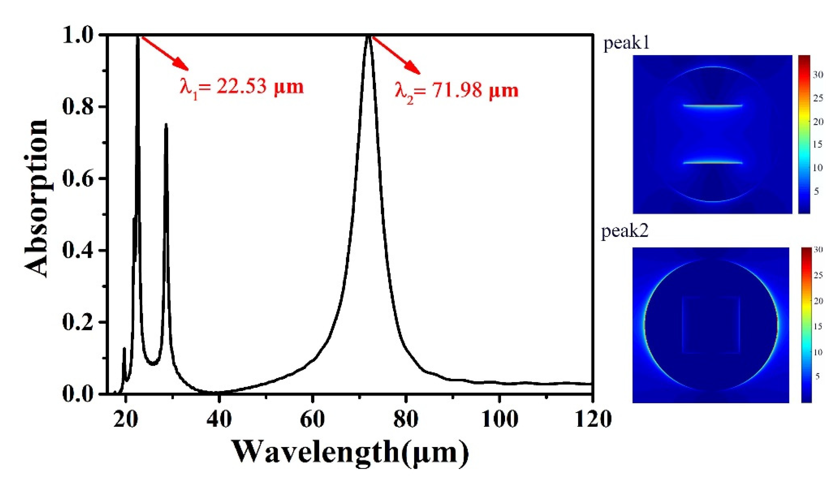
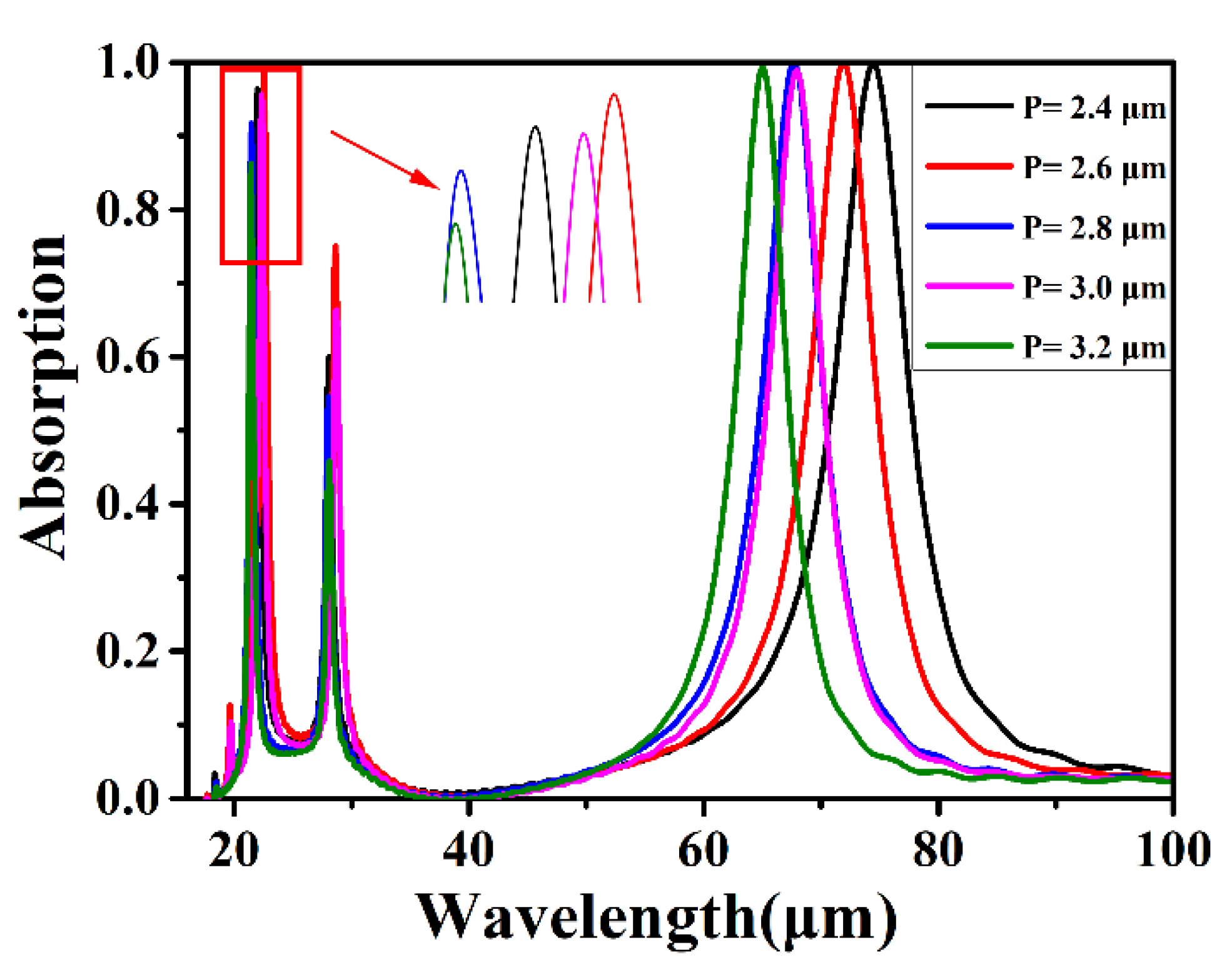
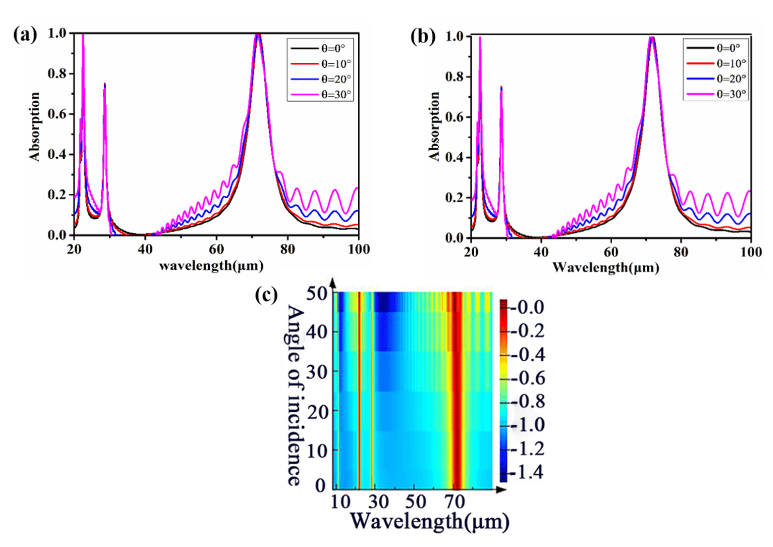
3. Simulation Results and Discussions

Figure 2a–c compare the absorption efficiency of a single disk/square structure graphene absorber and the “ancient coin”-type graphene absorber under normal incident conditions. It can be seen from Figure 2a that only one high-efficiency absorption peak appears in the single disk structure absorber, and the absorption efficiency is only 59.57%. Similarly, the single square structure shown in Figure 2b has only one high-efficiency absorption peak with an absorption of 76.30%. As for the “ancient coin” structure we proposed, as shown in Figure 2c, it has two perfect absorption peaks at λ1 = 22.53 μm and λ2 = 71.98 μm, and the absorption efficiency reaches 99.74% and 99.90%, which is very close to 100%. Therefore, it is easy to draw the conclusion that our proposed “ancient coin” structure greatly improves the absorption capacity of monolayer graphene for incident light. In order to explain this physical mechanism, we set-up separate monitors for the wavelengths corresponding to these two perfect absorption peaks. In Figure 3, the electric field distribution diagram of two peaks generated by the electric field |Ez| on the x-y plane is given. It demonstrates that the appearance of the maximum absorption peak is associated with the electric field distribution of the graphene disk and the excavated square part. Different contributions of the square and the disk to these two peaks are portrayed from the two graphs on the right side of Figure 3. At about 22.53 μm, the contribution of the horizontal edge of the square to their absorption is higher than the contribution of the disk, while at about 71.98 μm, the contribution of the edge of the graphene nanodisk is largest, and the square hardly contributes. From this, we can reach the conclusion that different resonance bands have different resonance regions.
The absorption bandwidth can be defined by the half-height width (also called FWHM), which refers to the corresponding spectral width when the peak height of the absorption band is half. The FWHMs of mode λ1 and mode λ2 are 0.96 and 0.99, respectively, through calculations. The absorption bandwidth is relatively narrow, which means that our absorber has a strong wavelength selectivity. In addition, the quality factor Q of the proposed structure was studied. It is a physical quantity that represents the relative bandwidth of the resonator’s vibration frequency. The higher the quality factor, the narrower the frequency range that can generate resonance, the longer the duration, and the better the stability. The quality factor Q can be obtained by the formula Q = λ/FWHM [69]. In our absorber, the Q factor of mode λ2 is 72.28, which is 3.07 times the Q factor of mode λ1, and it demonstrates that mode λ2 has more potential for application in the field of sensor than λ1.
Based on previous studies [63,70], we found that the absorptive capacity is closely relevant to the period P. Thus, in this part, we studied the relationship between the period P and the light absorption rate. Figure 4 suggests that different periods P show different changing trends of the two perfect absorption peaks. For mode λ1, as the period increases from 2.4 to 3.2 μm (each interval of 0.2 μm takes a value), the absorption efficiency increases first and then decreases to 86.26%. When P = 2.6 μm, the absorption efficiency reaches the maximum value of 99.74%, so the period was set to 2.6 μm in our work. In addition, the wavelength of the absorption peak remains almost unchanged with the increase in P, which is basically located at λ1 = 22.53 μm. This is because the resonance condition remains almost the same level, and the resonance peak wavelength changes slightly in a small range due to the influence of resonance caused by the horizontal edge of the square. For mode λ2, with the increase in period, the absorption efficiency is basically maintained at around 99% with hardly any fluctuation, while the absorption peak shows an obvious blueshift from 74.31 to 64.95 μm. The reason is that when the structure is illuminated by a plane wave with the electric field along the x- direction, the effective index of graphene surface plasmon polaritons along the x- direction decreases as P increases. The resonance wavelength also shifts to the shorter band as the wavelength is proportional to the effective index.
After that, the influence of the geometrical parameters of our proposed structure on the absorption rate attracted our attention, as shown in Figure 5. In Figure 5a, the curves of different color represent the absorption spectra of the absorber with different disk radii R. Here, the controlled variable method was used, with P = 2.6 μm and the side length of square L = 0.95 μm fixed. By increasing the value of R regularly, we explored the influence of disk radius on the overall absorption. It is apparent from Figure 5a that as R increases from 0.8 to 1.2 μm, the wavelengths of mode λ1 and mode λ2 experiences a blueshift first, and then a redshift, which shows that both modes are sensitive to the changes in R. Moreover, the absorption efficiency of two peaks shows the same trends of increasing first and then decreasing with the gradual increase in R. It is the increase in the ratio filled with graphene as the disk radius R increases that results in the enhancement of absorption capacity. However, when R is too large (over 1.1 μm), the absorption efficiency decreases as the structure is close to the adjacent graphene pattern units, and it can interact with each other.
Figure 5b illustrates the effect of the size of the hollowed-out square on the light absorption rate with period P and disk radius R constant. It can also be seen that as L increases from 0.90 to 1.10 μm in intervals of 0.05 μm, the resonance wavelength of mode λ1 changes slightly in a small range; this is the same physical mechanism as when P increases. However, the mode λ2 shows a redshift from 68.66 to 79.46 μm, which can be attributed to the increase in the effective index of graphene nanodisk surface plasmon polaritons due to the tighter distribution of electric fields. At the same time, the absorption efficiency of mode λ1 and mode λ2 increases first and then decreases. This is because, as the area of the square excavated increases, the internal arrangement of graphene becomes tighter, and the increased surface plasmon polaritons can lead to an increase in absorption efficiency to light. However, when L > 0.95 μm, the resonance peak excited between different regions interfere with each other, resulting in a reduction in the absorption efficiency. Through simulation, it was found that when R = 1.10 μm and L = 0.95 μm, the maximum absorption of two peaks can be obtained.
In Figure 6a, we explored the absorption performance on Ef of graphene. Here, the other geometric parameters we took are also consistent with Figure 1. Based on the existing literature, we learned that the concept of perfect absorption comes from electric dipole resonance and magnetic dipole resonance [71]. As Ef increases from 0.4 to 0.8 eV, the wavelengths of the two resonance peaks blueshift. The graphene resonator can be treated as a dipole antenna as the wavelength of incident light is much larger than the structural parameters of the model. Thus, the effective index of graphene surface plasmons decreases with Ef, resulting in a decline in the resonance wavelength. The absorption efficiency of the absorption peak shows a trend of first increasing and then decreasing. When Ef = 0.6 eV, both absorption peaks reach the maximum absorption efficiency. Therefore, in this paper, the Ef of graphene was set as 0.6 eV.
In Figure 6b, we discuss the influence of different relaxation times on the absorption rate, and the other parameters are the same as we used in Figure 1. The relaxation time of electrons in graphene can be calculated with the formula: τ = ( μ μ c ) / ( e ν F 2 ) , where e is the electron charge, νF = 106 m/s is the Fermi velocity, μc = 0.6 eV is the chemical potential, and μ is the carrier mobility. We can learn from the above formula that the relaxation time will increase with μ. Thus, in the simulation debugging, the relaxation time can be changed with the method of setting different μ. The result in this figure demonstrates that the width of the peak gradually narrows and the absorption rate gradually increases with the relaxation time. This is mainly because as τ increases, the plasmon oscillations absorption will increase with the contribution of charge carriers, leading to a higher absorption to light. When τ = 0.8 ps, the two absorption peaks both reach the maximum absorption value of over 99%. Thus, in this paper, the relaxation time was set to 0.8 ps.
Next, we studied the relationship between background refractive index (RI) and absorption rate. From Figure 7a, when RI increases from 1.0 to 1.5 (with an interval of 0.1), both the wavelengths corresponding to the two perfect absorption peaks redshift. Regarding the change in absorbance shown in Figure 7c, the result demonstrates that the absorption rate of the first peak decreases with RI, but the second absorption peak remains the same. In addition, the specific condition of the redshift in the wavelength is shown in Figure 7b. The result indicates that the resonance wavelengths corresponding to the two perfect absorption peaks linearly increase with the RI. It is clear from Figure 7b that the slope of the line corresponding to the wavelength λ2 is greater than the line corresponding to the wavelength λ1; therefore, the wavelength sensitivity of the perfect absorption peak λ2 is higher than λ1 as the slope can be used to express the wavelength sensitivity. The following formula can also be used to calculate the wavelength sensitivity of the two absorption peaks:
S   = P e a k s h i f t ( e v ) Δ R I U
This formula represents the ratio of shift values of the peak to the changes in RI. By entering the values, we can calculate that the sensitivity of wavelength λ1 is 5.6 μm/RIU, while the sensitivity of wavelength λ2 is 16.46 μm/RIU. The result is also consistent with the performance of the slope in Figure 7b, and the two figures can confirm each other. According to this property, we can see that the absorber structure we proposed has potential application value in sensors.
Finally, we analyzed the relationship between the angle and absorptive capacity of the absorber by adjusting the angle of incident light. Figure 8 shows the absorption condition of our proposed absorber structure under two incident light polarization modes (TM polarization and TE polarization). In Figure 8a, we set the polarization direction (angle phi) to 0 and gradually increased the value of θ from 0 to 30° to obtain the absorption spectra generated by the incident light at different angles under TM polarization. In Figure 8b, we set the polarization direction to 90° and took the same steps under TE polarization. We found that the half-height width, the wavelength of the resonant peak, and the maximum absorption efficiency shown in Figure 8a,b remained the same. It is the local plasmon resonance on the patterned graphene layer that results in the appearance of resonant peaks. The wavelength of the surface plasmons of the graphene nanostructure is also shorter than the vacuum wavelength of the incident light [72], for which reason the two resonant modes remained unchanged. The result demonstrates that the proposed structure does not depend on the polarization of incident light, which means the structure is not sensitive to the TM and TE polarization modes. In addition, Figure 8c provides evidence for this phenomenon. We scanned the polarization angle from 0° to 50°, and we added the reflectivity monitor and transmissivity monitor to detect absorption conditions. The two red bands represent two high absorption peaks. When the polarization angle increased from 0 to 50°, the center frequencies of the two high absorption bands did not change, which indicates that the structure is not sensitive to the polarization angle of light. The phenomenon can be attributed to the high symmetry of our proposed structure, which eliminates the internal polarization angle dependence. Therefore, the proposed absorber can be promising in many integrated optical devices.

4. Conclusions

An “ancient coin”-type dual-band tunable graphene metamaterial perfect absorber is proposed in this paper. By adjusting the geometric parameters of the structure, the Fermi level, and the relaxation time of the graphene, two continuously adjustable perfect absorption peaks were obtained, which reached an absorption rate of over 99% at 22.53 and 71.98 μm. In addition, by investigating the background refractive index of the “ancient coin” structure, the result indicated that the maximum absorption efficiency corresponding to wavelength λ1 decreased with the refractive index, while the maximum absorption efficiency corresponding to wavelength λ2 had little change. At the same time, the sensitivities of wavelength λ1 and wavelength λ2 were 5.6 and 16.46 μm/RIU, respectively. Finally, we changed the polarization direction and incident angle, and we found that the two perfect absorption peaks of the absorber always remained in the state of maximum absorption, that is, our structure has good angular polarization tolerance. Compared with previous devices, our structure has broad application prospects in biosensing, photoelectric detection, and other fields due to its good refractive index sensitivity, good angular polarization tolerance, and highly symmetrical configuration.

Author Contributions

Conceptualization, H.L. and Q.S.; data curation, H.L., Q.S. and Y.Y. (Yinting Yi); formal analysis, Y.Y. (Yougen Yi) and Z.L.; methodology, H.L., Q.S., Y.Y. (Yinting Yi), Y.Y. (Yougen Yi) and Z.L.; resources, Y.Y. (Yougen Yi); software, Y.Y. (Yougen Yi), S.C. and Z.L.; data curation, H.L.; writing—original draft preparation, H.L.; writing—review and editing, H.L. and Y.Y. (Yougen Yi). All authors have read and agreed to the published version of the manuscript.

Funding

The authors are grateful to the support by the National Natural Science Foundation of China (NSFC) (11904032, 11774054, 12075036), the Scientific Research Plan of the Provincial Education Department in Hubei (Q20161309), and the Natural Science Foundation of Hunan Province (2019JJ50133).

Institutional Review Board Statement

Not applicable.

Informed Consent Statement

Not applicable.

Data Availability Statement

Publicly available datasets were analyzed in this study. This data can be found here: [https://www.lumerical.com/], accessed on 1 January 2021.

Conflicts of Interest

The authors declare no conflict of interest.

References

  1. Walser, R.M. Electromagnetic metamaterials. Complex Mediums II: Beyond Linear Isotropic Dielectrics; International Society for Optics and Photonics: Bellingham, WA, USA, 2001; Volume 4467, pp. 1–16. [Google Scholar] [CrossRef]
  2. Chen, Z.; Chen, H.; Jile, H.; Xu, D.; Yi, Z.; Lei, Y.; Chen, X.; Zhou, Z.; Cai, S.; Li, G. Multi-band multi-tunable perfect plasmon absorber based on L-shaped and double-elliptical graphene stacks. Diam. Relat. Mater. 2021, 115, 108374. [Google Scholar] [CrossRef]
  3. Liu, Z.; Zhang, X.; Zhou, F.; Luo, X.; Zhang, Z.; Qin, Y.; Zhuo, S.; Gao, E.; Li, H.; Yi, Z. Triple plasmon-induced transparency and optical switch desensitized to polarized light based on a mono-layer metamaterial. Opt. Express 2021, 29, 13949–13959. [Google Scholar] [CrossRef] [PubMed]
  4. Cheng, T.; Gao, W.; Gao, H.; Wang, S.; Yi, Z.; Wang, X.; Yang, H. Piezocatalytic degradation of methylene blue, tetrabromobisphenol A and tetracycline hydrochloride using Bi4Ti3O12 with different morphologies. Mater. Res. Bull. 2021, 141, 111350. [Google Scholar] [CrossRef]
  5. He, Z.; Li, L.; Ma, H.; Pu, L.; Xu, H.; Yi, Z.; Cao, X.; Cui, W. Graphene-based metasurface sensing applications in terahertz band. Results Phys. 2021, 21, 103795. [Google Scholar] [CrossRef]
  6. An, S.; Lv, J.; Yi, Z.; Liu, C.; Yang, L.; Wang, F.; Liu, Q.; Su, W.; Li, X.; Sun, T.; et al. Ultra-short and dual-core photonic crystal fiber polarization splitter composed of metal and gallium arsenide. Optik 2021, 226, 165779. [Google Scholar] [CrossRef]
  7. Wang, X.X.; Zhu, J.K.; Xu, Y.Q.; Qi, Y.P.; Zhang, L.P.; Yang, H.; Yi, Z. A novel plasmonic refractive index sensor based on gold/silicon complementary grating structure. Chin. Phys. B 2021, 30, 024207. [Google Scholar] [CrossRef]
  8. Wang, Y.; Yi, Y.; Xu, D.; Yi, Z.; Li, Z.; Chen, X.; Jile, H.; Zhang, J.; Zeng, L.; Li, G. Terahertz tunable three band narrowband perfect absorber based on Dirac semimetal. Phys. E Low-Dimens. Syst. Nanostruct. 2021, 131, 114750. [Google Scholar] [CrossRef]
  9. Qi, Y.; Zhang, B.; Ding, J.; Zhang, T.; Wang, X.; Yi, Z. Efficient Manipulation of Terahertz waves by multi-bit Coding Metasurfaces and its further application. Chin. Phys. B 2021, 30, 024211. [Google Scholar] [CrossRef]
  10. Li, J.; Chen, X.; Yi, Z.; Yang, H.; Tang, Y.; Yi, Y.; Yao, W.; Wang, J.; Yi, Y. Broadband solar energy absorber based on monolayer molybdenum disulfide using tungsten elliptical arrays. Mater. Today Energy 2020, 16, 100390. [Google Scholar] [CrossRef]
  11. Wang, X.X.; Tong, H.; Pang, Z.Y.; Zhu, J.K.; Wu, X.X.; Yang, H.; Qi, Y. Theoretical realization of three-dimensional nanolattice structure fabrication based on high-order waveguide-mode interference and sample rotation. Opt. Quant. Electron. 2019, 51, 38. [Google Scholar] [CrossRef]
  12. Chen, Z.; Chen, H.; Yin, J.; Zhang, R.; Jile, H.; Xu, D.; Yi, Z.; Zhou, Z.; Cai, S.; Yan, P. Multi-band, Tunable, High Figure of Merit, High Sensitivity Single-layer Patterned Graphene—Perfect Absorber Based On Surface Plasmon Resonance. Diam. Relat. Mater. 2021, 116, 108393. [Google Scholar] [CrossRef]
  13. Deng, Y.; Cao, G.T.; Yang, H.; Zhou, X.Q.; Wu, Y.W. Dynamic Control of Double Plasmon-Induced Transparencies in Aperture-Coupled Waveguide-Cavity System. Plasmonics 2018, 13, 345–352. [Google Scholar] [CrossRef]
  14. Long, F.; Zhang, Z.H.; Wang, J.; Yan, L.; Zhou, B.W. Cobalt-nickel bimetallic nanoparticles decorated graphene sensitized imprinted electrochemical sensor for determination of octylphenol. Electrochim. Acta 2015, 168, 337–345. [Google Scholar] [CrossRef]
  15. Yao, J.; Liu, Z.; Liu, Y.; Wang, Y.; Sun, C.; Bartal, G.; Stacy, A.M.; Zhang, X. Optical negative refraction in bulk metamaterials of nanowires. Science 2008, 321, 930. [Google Scholar] [CrossRef] [PubMed]
  16. Zhang, Z.H.; Cai, R.; Long, F.; Wang, J. Development and application of tetrabromobisphenol A imprinted electrochemical sensor based on graphene/carbon nanotubes three-dimensional nanocomposites modified carbon electrode. Talanta 2015, 134, 435–442. [Google Scholar] [CrossRef] [PubMed]
  17. Chen, H.J.; Zhang, Z.H.; Cai, R.; Kong, X.Q.; Chen, X.; Liu, Y.N.; Yao, S.Z. Molecularly imprinted electrochemical sensor based on a reduced graphene modified carbon electrode for tetrabromobisphenol A detection. Analyst 2013, 138, 2769–2776. [Google Scholar] [CrossRef]
  18. Zhang, Y.; Yi, Z.; Wang, X.; Chu, P.; Yao, W.; Zhou, Z.; Cheng, S.; Liu, Z.; Wu, P.; Pan, M.; et al. Dual band visible metamaterial absorbers based on four identical ring patches. Phys. E Low-Dimens. Syst. Nanostruct. 2021, 127, 114526. [Google Scholar] [CrossRef]
  19. Chen, X.; Wu, W.; Zhang, W.; Wang, Z.; Fu, Z.; Zhou, L.; Yi, Z.; Li, G.; Zeng, L. Blue and green double band luminescent carbon quantum dots: Synthesis, origin of photoluminescence, and application in white light-emitting devices. Appl. Phys. Lett. 2021, 118, 153102. [Google Scholar] [CrossRef]
  20. Yi, Z.; Li, J.K.; Lin, J.C.; Qin, F.; Chen, X.F.; Yao, W.T.; Liu, Z.M.; Cheng, S.B.; Wu, P.H.; Li, H.L. Broadband polarization-insensitive and wide-angle solar energy absorber based on tungsten ring-disc array. Nanoscale 2020, 12, 23077–23083. [Google Scholar] [CrossRef]
  21. Cheng, Z.H.; Liao, J.; He, B.Z.; Zhang, F.; Zhang, F.A.; Huang, X.H.; Zhou, L. One-Step Fabrication of Graphene Oxide Enhanced Magnetic Composite Gel for Highly Efficient Dye Adsorption and Catalysis. ACS Sustain. Chem. Eng. 2015, 3, 1677–1685. [Google Scholar] [CrossRef]
  22. Landy, N.I.; Sajuyigbe, S.; Mock, J.J.; Smith, D.R.; Padilla, W.J. Perfect metamaterial absorber. Phys. Rev. Lett. 2008, 100, 207402. [Google Scholar] [CrossRef]
  23. Chu, P.X.; Chen, J.X.; Xiong, Z.G.; Yi, Z. Controllable frequency conversion in the coupled time-modulated cavities with phase delay. Opt. Commun. 2020, 476, 126338. [Google Scholar] [CrossRef]
  24. Cai, R.; Rao, W.; Zhang, Z.H.; Long, F.; Yin, Y.L. An imprinted electrochemical sensor for bisphenol A determination based on electrodeposition of a graphene and Ag nanoparticle modified carbon electrode. Anal. Methods 2014, 6, 1590–1597. [Google Scholar] [CrossRef]
  25. Jiang, L.Y.; Yi, Y.T.; Yi, Z.; Yang, H.; Li, Z.Y.; Su, J.; Zhou, Z.G.; Chen, X.F.; Yi, Y.G. A four-band perfect absorber based on high quality factor and high figure of merit of monolayer molybdenum disulfide. Acta Phys. Sin. 2021, 70, 128101. [Google Scholar] [CrossRef]
  26. Pan, M.; Huang, H.Z.; Chen, W.Z.; Li, S.; Xie, Q.; Xu, F.; Wei, D.; Fang, J.; Fan, B.; Cai, L. Design of narrow-band absorber based on symmetric silicon grating and research on its sensing performance. Coatings 2021, 11, 553. [Google Scholar] [CrossRef]
  27. Xu, L.; Zeng, J.; Luo, X.; Xia, L.; Ma, Z.; Peng, B.; Li, Z.; Zhai, X.; Wang, L. Dual-Band Plasmonic Perfect Absorber Based on the Hybrid Halide Perovskite in the Communication Regime. Coatings 2021, 11, 67. [Google Scholar] [CrossRef]
  28. Liu, X.; Tyler, T.; Starr, T.; Starr, A.F.; Jokerst, N.M.; Padilla, W.J. Taming the blackbody with infrared metamaterials as selective thermal emitters. Phys. Rev. Lett. 2011, 107, 045901. [Google Scholar] [CrossRef] [PubMed] [Green Version]
  29. Zhang, X.; Liu, Z.; Zhang, Z.; Qin, Y.; Zhuo, S.; Luo, X.; Zhou, F.; Yi, Z.; Wang, J.; Wang, Y. Triple plasmon-induced transparency in graphene and metal metamaterials and its anomalous property. J. Phys. D Appl. Phys. 2021, 54, 284001. [Google Scholar] [CrossRef]
  30. Chen, H.; O’Hara, J.F.; Azad, A.K.; Taylor, A.J.; Averitt, R.D. Experimental demonstration of frequency-agile terahertz metamaterials. Nat. Photonics 2008, 2, 295–298. [Google Scholar] [CrossRef]
  31. Zhang, Z.; Liu, Z.; Zhou, F.; Wang, J.; Wang, Y.; Zhang, X.; Qin, Y.; Zhuo, S.; Luo, X.; Gao, E.; et al. Broadband plasmon-induced transparency modulator in the terahertz band based on multilayer graphene metamaterials. JOSA A 2021, 38, 784–789. [Google Scholar] [CrossRef]
  32. Deng, Y.; Cao, G.; Wu, Y.; Zhou, X.; Liao, W. Theoretical Description of Dynamic Transmission Characteristics in MDM Waveguide Aperture-Side-Coupled with Ring Cavity. Plasmonics 2015, 10, 1537–1543. [Google Scholar] [CrossRef]
  33. Cao, G.; Li, H.; Deng, Y.; Zhan, S.; He, Z.; Li, B. Systematic Theoretical Analysis of Selective-Mode Plasmonic Filter Based on Aperture-Side-Coupled Slot Cavity. Plasmonics 2014, 9, 1163–1169. [Google Scholar] [CrossRef]
  34. Driscoll, T.; Palit, S.; Qazilbash, M.M.; Brehm, M.; Keilmann, F.; Chae, B.-G.; Yun, S.-J.; Kim, H.T.; Cho, S.-Y.; Jokerst, N.M.; et al. Dynamic tuning of an infrared hybrid-metamaterial resonance using vanadium dioxide. Appl. Phys. Lett. 2008, 93, 18. [Google Scholar] [CrossRef]
  35. Novoselov, K.S.; Fal’ko, V.I.; Colombo, L.; Gellert, P.R.; Kim, K.A. A roadmap for graphene. Nature 2012, 490, 192–200. [Google Scholar] [CrossRef]
  36. Lin, X.; Li, Y.J.; Chen, F.T.; Xu, P.; Li, M. Facile synthesis of mesoporous titanium dioxide doped by Ag-coated graphene with enhanced visible-light photocatalytic performance for methylene blue degradation. RSC Adv. 2017, 7, 25314–25324. [Google Scholar] [CrossRef] [Green Version]
  37. Tang, N.M.; Li, Y.J.; Chen, F.T.; Han, Z.Y. In situ fabrication of a direct Z-scheme photocatalyst by immobilizing CdS quantum dots in the channels of graphene-hybridized and supported mesoporous titanium nanocrystals for high photocatalytic performance under visible light. RSC Adv. 2018, 8, 42233–42245. [Google Scholar] [CrossRef] [Green Version]
  38. Yang, X.; Zhang, F.; Hu, Y.J.; Chen, D.Z.; He, Z.Q.; Xiong, L.Z. Gold Nanoparticals Doping Graphene Sheets Nanocomposites Sensitized Screen-printed Carbon Electrode as a Disposable Platform for Voltammetric Determination of Guaiacol in Bamboo Juice. Int. J. Electrochem. Sci. 2014, 9, 5061–5072. [Google Scholar]
  39. Koppens, F.H.L.; Chang, D.E.; Thongrattanasiri, S.; de Abajo, F.J.G. Graphene plasmonics: A platform for strong light-matter interactions. Nano Lett. 2011, 11, 3370–3377. [Google Scholar] [CrossRef] [PubMed] [Green Version]
  40. Christensen, J.; Manjavacas, A.; Thongrattanasiri, S.; Koppens, F.H.H.; de Abajo, F.J.G. Graphene plasmon waveguiding and hybridization in individual and paired nanoribbons. ACS Nano 2012, 6, 431–440. [Google Scholar] [CrossRef] [Green Version]
  41. Long, F.; Zhang, Z.H.; Wang, J.; Yan, L.; Lu, P.P.; Yang, Z.X. Magnetic Graphene Modified Imprinted Electrochemical Sensor for Detection of 4-Octylphenol. Chin. J. Anal. Chem. 2016, 44, 908–914. [Google Scholar] [CrossRef]
  42. Zhou, Q.; Ju, W.; Yong, Y.; Zhang, Q.; Liu, Y.; Li, J. Effect of the N/P and transition-metal co-doping on the quantum capacitance of supercapacitor electrodes based on mono- and multilayer graphene. Carbon 2020, 170, 368–379. [Google Scholar] [CrossRef]
  43. Cen, C.L.; Zhang, Y.B.; Chen, X.F.; Yang, H.; Yi, Z.; Yao, W.T.; Tang, Y.J.; Yi, Y.G.; Wang, J.Q.; Wu, P.H. A dual-band metamaterial absorber for graphene surface plasmon resonance at terahertz frequency. Phys. E 2020, 117, 113840. [Google Scholar] [CrossRef]
  44. Wang, X.; Duan, J.; Chen, W.; Zhou, C.; Liu, T.; Xiao, S. Controlling light absorption of graphene at critical coupling through magnetic dipole quasi-bound states in the continuum resonance. Phys. Rev. B 2021, 102, 155432. [Google Scholar] [CrossRef]
  45. Chen, J.; Nie, H.; Peng, C.; Qi, S.B.; Tang, C.J.; Zhang, Y.; Wang, L.H.; Park, G.S. Enhancing the Magnetic Plasmon Resonance of three-dimensional optical Metamaterials via Strong Coupling for High-Sensitivity Sensing. J. Light. Technol. 2018, 36, 3481. [Google Scholar] [CrossRef]
  46. Jiang, L.; Yuan, C.; Li, Z.; Su, J.; Yi, Z.; Yao, W.; Wu, P.; Liu, Z.; Cheng, S.; Pan, M. Multi-band and high-sensitivity perfect absorber based on monolayer grapheme metamaterial. Diam. Relat. Mater. 2021, 111, 108227. [Google Scholar] [CrossRef]
  47. Li, J.H.; Jiang, J.B.; Zhao, D.; Xu, Z.F.; Liu, M.Q.; Liu, X.; Tong, H.X.; Qian, D. Novel hierarchical sea urchin-like Prussian blue@palladium core-shell heterostructures supported on nitrogen-doped reduced graphene oxide: Facile synthesis and excellent guanine sensing performance. Electrochim. Acta 2020, 330, 135196. [Google Scholar] [CrossRef]
  48. Cai, L.; Zhang, Z.H.; Xiao, H.M.; Chen, S.; Fu, J.L. An eco-friendly imprinted polymer based on graphene quantum dots for fluorescent detection of p-nitroaniline. RSC Adv. 2019, 9, 41383–41391. [Google Scholar] [CrossRef] [Green Version]
  49. Yu, P.; Yang, H.; Chen, X.; Yi, Z.; Yao, W.; Chen, J.; Yi, Y.; Wu, P. Ultra-wideband solar absorber based on refractory titanium metal. Renew. Energy 2020, 158, 227–235. [Google Scholar] [CrossRef]
  50. Yang, M.; Kong, Q.; Feng, W.; Yao, W. N/O double-doped biomass hard carbon material realizes fast and stable potassium ion storage. Carbon 2021, 176, 71–82. [Google Scholar] [CrossRef]
  51. He, Z.; Li, L.; Cui, W.; Wang, Y.; Xue, W.; Xu, H.; Yi, Z.; Li, C.; Li, Z. Unidirectional reflectionless propagation of near-infrared light in resonator-assisted non-parity-time symmetric waveguides. New J. Phys. 2021, 23, 053015. [Google Scholar] [CrossRef]
  52. Zhang, B.; Qi, Y.; Zhang, T.; Zhang, Y.; Liu, W.; Wang, L.; Ding, J.; Wang, X.; Yi, Z. Tunable multi-band terahertz absorber based on composite graphene structures with square ring and Jerusalem cross. Results Phys. 2021, 25, 104233. [Google Scholar] [CrossRef]
  53. Zhang, X.; Liu, Z.; Zhang, Z.; Gao, E.; Luo, X.; Zhou, F.; Li, H.; Yi, Z. Polarization-sensitive triple plasmon-induced transparency with synchronous and asynchronous switching based on monolayer graphene metamaterials. Opt. Express 2020, 28, 36771–36783. [Google Scholar] [CrossRef]
  54. Wang, Y.; Cui, W.; Ma, H.; Xu, H.; Yi, Z.; Cao, X.; Ren, X.; He, Z. Outstanding slow-light effect for graphene metasurface in terahertz. Results Phys. 2021, 23, 104002. [Google Scholar] [CrossRef]
  55. Li, J.H.; Jiang, J.B.; Xu, Z.F.; Liu, M.Q.; Tang, S.P.; Yang, C.M.; Qian, D. Facile synthesis of Ag@Cu2O heterogeneous nanocrystals decorated N-doped reduced graphene oxide with enhanced electrocatalytic activity for ultrasensitive detection of H2O2. Sens. Actuators B Chem. 2018, 260, 529–540. [Google Scholar] [CrossRef]
  56. Zhou, Q.; Ju, W.; Yong, Y.; Liu, Y.; Li, J. Quantum capacitance of supercapacitor electrodes based on germanene influenced by vacancy and co-doping: A first-principles study. Comput. Mater. Sci. 2021, 188, 110131. [Google Scholar] [CrossRef]
  57. Zhang, Y.; Feng, Y.; Zhu, B.; Zhao, J.; Jiang, T. Graphene based tunable metamaterial absorber and polarization modulation in terahertz frequency. Opt. Exp. 2014, 22, 22743–22752. [Google Scholar] [CrossRef] [PubMed]
  58. Su, Z.; Yin, J.; Zhao, X. Terahertz dual-band metamaterial absorber based on graphene/MgF2 multilayer structures. Opt. Exp. 2015, 23, 1679–1690. [Google Scholar] [CrossRef] [PubMed]
  59. Yao, G.; Ling, F.; Yue, J.; Luo, C.; Ji, J.; Yao, J. Dual-band tunable perfect metamaterial absorber in the THz range. Opt. Express 2016, 24, 1518–1527. [Google Scholar] [CrossRef] [PubMed]
  60. Li, H.G.; Ji, C.S.; Ren, Y.Z.; Hu, J.; Qin, M.; Wang, L. Investigation of multiband plasmonic metamaterial perfect absorbers based on graphene ribbons by the phase-coupled method. Carbon 2019, 141, 481–487. [Google Scholar] [CrossRef]
  61. Yao, Y.; Liao, Z.; Liu, Z.; Liu, X.; Zhou, J.; Liu, G.; Yi, Z.; Wang, J. Recent progresses on metamaterials for optical absorption and sensing: A review. J. Phys. D Appl. Phys. 2021, 54, 113002. [Google Scholar] [CrossRef]
  62. Huang, X.; Yang, F.; Gao, B.; Yang, Q.; Wu, J.; He, W. Metamaterial absorber with independently tunable amplitude and frequency in the terahertz regime. Opt. Express 2019, 27, 25902–25911. [Google Scholar] [CrossRef] [PubMed]
  63. Ke, S.L.; Wang, B.; Huang, H.; Long, H.; Wang, K.; Lu, P.X. Plasmonic absorption enhancement in periodic cross-shaped graphene arrays. Opt. Express 2015, 23, 8888–8900. [Google Scholar] [CrossRef] [PubMed]
  64. Rodrigo, D.; Limaj, O.; Janner, D.; Etezadi, D.; de Abajo, F.J.G.; Pruneri, V.; Altug, H. Mid-infrared plasmonic biosensing with graphene. Science 2015, 349, 165–168. [Google Scholar] [CrossRef] [PubMed] [Green Version]
  65. Yu, J.; Zhu, J.; Ye, S.; Wang, X. Ultra-wide sensing range plasmonic refractive index sensor based on a two-dimensional circular-hole grating engraved on a gold film. Results Phys. 2021, 26, 104396. [Google Scholar] [CrossRef]
  66. Xiang, Y.J.; Dai, X.Y.; Guo, J.; Zhang, H.; Wen, S.; Tang, D. Critical coupling with graphene-based hyperbolic metamaterials. Sci. Rep. 2014, 4, 5483. [Google Scholar] [CrossRef] [Green Version]
  67. Christopoulos, T.; Tsilpakos, O.; Sinatkas, G.; Kriezis, E.E. On the calculation of the quality factor in contemporary photonic resonant structures. Opt. Express 2019, 360479. [Google Scholar] [CrossRef] [Green Version]
  68. Shuang, W.; Sheng, L.J. Hollow-petal graphene metasurface for broadband tunable THz absorption. Appl. Opt. 2019, 58, 3023–3028. [Google Scholar] [CrossRef]
  69. Wang, J.; Hu, C.P.; Tian, Q.; Yu, W.X.; Tian, H.H. Ultrahigh-Q and polarization-independent terahertz metamaterial perfect absorber. Plasmonics 2020, 15, 1943–1947. [Google Scholar] [CrossRef]
  70. Wu, D.; Wang, M.; Feng, H.; Xu, Z.; Liu, Y.; Xia, F.; Zhang, K.; Kong, W.; Dong, L.; Yun, M. Independently tunable perfect absorber based on the plasmonic in double-layer graphene structure. Carbon 2019, 155, 618–623. [Google Scholar] [CrossRef]
  71. Zhou, N.; Xu, X.F. Metamaterial-based perfect absorbers for efficiently enhancing near field radiative heat transfer. J. Quant. Spectrosc. Radiat. Transf. 2015, 167, 156–163. [Google Scholar] [CrossRef] [Green Version]
  72. Zhang, J.; Zhu, Z.; Liu, W.; Yuan, X.; Qin, S. Towards photodetection with high efficiency and tunable spectral selectivity: Graphene plasmonics for light trapping and absorption engineering. Nanoscale 2015, 7, 13530–13536. [Google Scholar] [CrossRef] [PubMed]
Figure 1. Three-dimensional schematic diagram of “ancient coin”-type periodic graphene perfect absorber (four units). The bottom layer is a silicon (Si) semiconductor layer as a semi-infinite (i.e., t1 = ∞) substrate. The thickness of the second Ag layer and the third silicon dioxide (SiO2) layer are t2 = 0.465 μm and t3 = 4.1 μm, respectively. The geometric parameters of the “ancient coin”-type structure are: radius of the circle R = 1.1 μm; side length of the hollowed-out square L = 0.95 μm; thickness of the graphene array of 1 nm. The period of the proposed structure is P = Px = Py = 2.6 μm.
Coatings 11 00814 g001
Figure 2. (a) A schematic diagram of light absorption of a single-disc-structure graphene absorber and a planform of the absorber, with radius R and period P. (b) A schematic diagram of light absorption of a single-square-structure graphene absorber and a planform of the absorber, with side length L and period P. (c) The light absorption diagram and planform of the “ancient coin” graphene absorber.
Coatings 11 00814 g002
Figure 3. The optical absorption spectrum of the “ancient coin” structure and the corresponding electric field diagrams of the two perfect absorption peaks on the x-y plane.
Coatings 11 00814 g003
Figure 4. Absorption spectrum of “ancient coin”-type absorber under different periods P.
Coatings 11 00814 g004
Figure 5. (a) The relationship between the radius R of the disc and the light absorption rate. (b) The relationship between the side length L of the square and the light absorption.
Coatings 11 00814 g005
Figure 6. (a) Absorption spectra corresponding to different Fermi levels Ef. (b) Absorption spectra corresponding to different relaxation times.
Coatings 11 00814 g006
Figure 7. (a) Absorption spectra under different background refractive indices. (b) The function relationship between the wavelengths of two perfect absorption peaks and the background refractive index. (c) The relationship between the absorption rate of two perfect absorption peaks and the background refractive index.
Coatings 11 00814 g007
Figure 8. (a) The generated spectra at different incident angles of light under TM polarization. (b) The generated spectra at different incident angles of light under TE polarization. (c) Scanning graph of the absorbance of the two peaks at different polarization azimuths.
Coatings 11 00814 g008
Publisher’s Note: MDPI stays neutral with regard to jurisdictional claims in published maps and institutional affiliations.

