Article

Characterization of Ultra-Thin Diamond-Like Carbon Films by SEM/EDX

by
Chanida Puttichaem
1,2,3,
Guilherme P. Souza
1,*,
Kurt C. Ruthe
1 and
Kittipong Chainok
2,3
1
Western Digital Storage Technologies (Thailand) Ltd., Klongjig, BangPa-In, Ayutthaya 13160, Thailand
2
Department of Materials and Textile Technology, Faculty of Science and Technology, Thammasat University, Pathum Thani 12120, Thailand
3
Thammasat University Research Unit in Multifunctional Crystalline Materials and Applications (TU-MCMA), Faculty of Science and Technology, Thammasat University, Pathum Thani 12121, Thailand
*
Author to whom correspondence should be addressed.
Coatings 2021, 11(6), 729; https://doi.org/10.3390/coatings11060729
Submission received: 17 May 2021 / Revised: 12 June 2021 / Accepted: 15 June 2021 / Published: 17 June 2021
(This article belongs to the Section Surface Characterization, Deposition and Modification)

Abstract

:
A novel, high throughput method to characterize the chemistry of ultra-thin diamond-like carbon films is discussed. The method uses surface sensitive SEM/EDX to provide substrate-specific, semi-quantitative silicon nitride/DLC stack composition of protective films extensively used in the hard disk drives industry and at Angstrom-level. SEM/EDX output is correlated to TEM to provide direct, gauge-capable film thickness information using multiple regression models that make predictions based on film constituents. The best model uses the N/Si ratio in the films, instead of separate Si and N contributions. Topography of substrate/film after undergoing wear is correlatively and compositionally described based on chemical changes detected via the SEM/EDX method without the need for tedious cross-sectional workflows. Wear track regions of the substrate have a film depleted of carbon, as well as Si and N in the most severe cases, also revealing iron oxide formation. Analysis of film composition variations around industry-level thicknesses reveals a complex interplay between oxygen, silicon and nitrogen, which has been reflected mathematically in the regression models, as well as used to provide valuable insights into the as-deposited physics of the film.

1. Introduction

Diamond-like carbon (DLC) is an amorphous carbon film with interesting properties, such as high mechanical strength and chemical inertness and is extensively used as protective coating in many industries, ranging from automotive to electronics. In hard disk drives (HDD), the function of the DLC film is to protect substrates against tribological wear and corrosion that could result in critical surface damage and related device failure [1]. In the HDD industry, read-write heads must fly in very close proximity to the media disks (i.e., minimal spacing allowance) to achieve high areal density or high storage capacity, and for that reason DLC overcoats on both head and media must meet wear and corrosion resistance at the <20 Å thickness regime [2]. Internal stress reduction and adhesion enhancement between the DLC film and substrate can be achieved by adding a “seed layer” [3,4]. Various seed layer systems have been tested, including metals (Ti, Al, Cr, W) [5,6,7], ceramics (SiO2, SiC, TiC, Si3N4, CrN) [8,9,10], and more complex composite systems [11]. Silicon nitride seeds have been found to be particularly promising in maintaining film stability under tribological stress regimes [12,13]. Following the total film thickness constraints, the seed layer has to be likewise kept as thin as possible [14]. Industrial scale characterization for quality inspection of such ultra-thin films, both in terms of composition and thickness, is incredibly challenging.
Developing sensitive, high throughput chemical/structural characterization tools for DLC films down to a few atomic layers thick is one of the most critical ambitions for new technology development and production quality control [15,16]. Many characterization techniques for DLC films have been reported in the literature. Well known techniques are: X-ray Diffraction (XRD), Transmission Electron Microscopy (TEM), Electron Energy Loss Spectroscopy (EELS), Raman Spectroscopy, X-ray Photoelectron Spectroscopy (XPS), Auger Electron Spectroscopy (AES), and Spectroscopic Ellipsometry (SE) [17,18,19,20]. Each of those techniques has advantages and disadvantages in different aspects. For example, TEM/EELS can provide both physical and chemical information, where the cross-sectioned film is analyzed throughout its stack, starting from the substrate until the film/air interface [18,19]. However, the technique is limited in terms of sampling and throughput, as samples have to be made in the form of thin foils via elaborate sub-micron scale cross-sectioning/thinning workflows. X-ray Reflectometry (XRR) can provide reliable film thickness only if physical properties such as density are well known. SE is often used as an in-situ monitor that relies on models and/or empirical correlations to TEM [20,21], whereas X-ray Fluorescence (XRF) and AES provide chemical characterization but are often challenged to some low concentration elements, which is often the case for DLC film compositions. It is worth noting that, in general, X-ray beam techniques cannot be used on HDD head’s functional substrates due to probe size limitations (i.e., the probe size is too large relative to the region of interest), which is not the case for the higher lateral resolution and small probe sizes readily available on electron-beam probe techniques. One such substrate is a ferromagnetic NiFe metal shield that surrounds and protects the nano-scale read and write devices against extraneous magnetic fields from adjacent data tracks on the media.
Characterization of DLC films with Scanning Electron Microscopy/X-ray Energy Dispersive Spectroscopy (SEM/EDX) has been, historically, limited to relatively thick films and with a stronger focus on film/surface morphology rather than compositional analysis [22]. Such studies often describe high incident electron energies to compensate for the low X-ray yield of carbon and/or accompanying interlayer materials, resulting in appreciable penetration depths and emphasis on detecting substrate materials rather than the coating itself [23]. In the present manuscript we report original research on the use of modern surface-sensitive SEM and windowless EDX with low noise electronics [24] to characterize industry-level, ultra-thin DLC films with a silicon nitride seed layer on actual HDD head NiFe substrates. The EDX experiments are performed at very low incident electron beam energies in a way to approach the conversion of the film-on-substrate situation (i.e., the electron beam penetrates through the film and into the substrate) back into a bulk analysis situation (i.e., electron beam only interacts with the film, and not with the substrate), as described in [25]. However, since the films are typically within the <30 Å thickness range, such condition is not feasible as the critical ionization energies for useful atom shells in the film elements are higher than permissible beam energies for that thickness range, and as a result both film and substrate X-rays are produced. We demonstrate the near-Angstrom level sensitivity of the technique and develop a simplified semi-quantitative ratio method. A correlation model between the SEM/EDX ratios with direct, TEM-based film thickness is presented, and the technique is also evaluated from a thin film metrology gauge-capability standpoint.
The overall structure of the study follows the rationale: (1) DLC films of varying silicon nitride, carbon, and oxygen contamination are deposited on HDD heads; (2) semi-quantitative analysis of the films is produced by SEM/EDX; (3) TEM image-based thickness for the same films is correlated to their chemical composition by SEM/EDX to build a compositional-based thickness model; (4) the model is applied to predict local film thickness changes on a head with DLC wear tracks.

2. Materials and Methods

2.1. DLC Films

DLC films produced via the filtered cathodic arc (FCA) process [26] were deposited on a Ni80Fe20 ferromagnetic HDD read-write head (NiFe) substrate. Prior to film deposition, NiFe substrates were subjected to lapping (i.e., a mechanical process for material removal), chemical cleaning and plasma etching to produce smooth, clean surfaces. The films produced followed the following scheme:
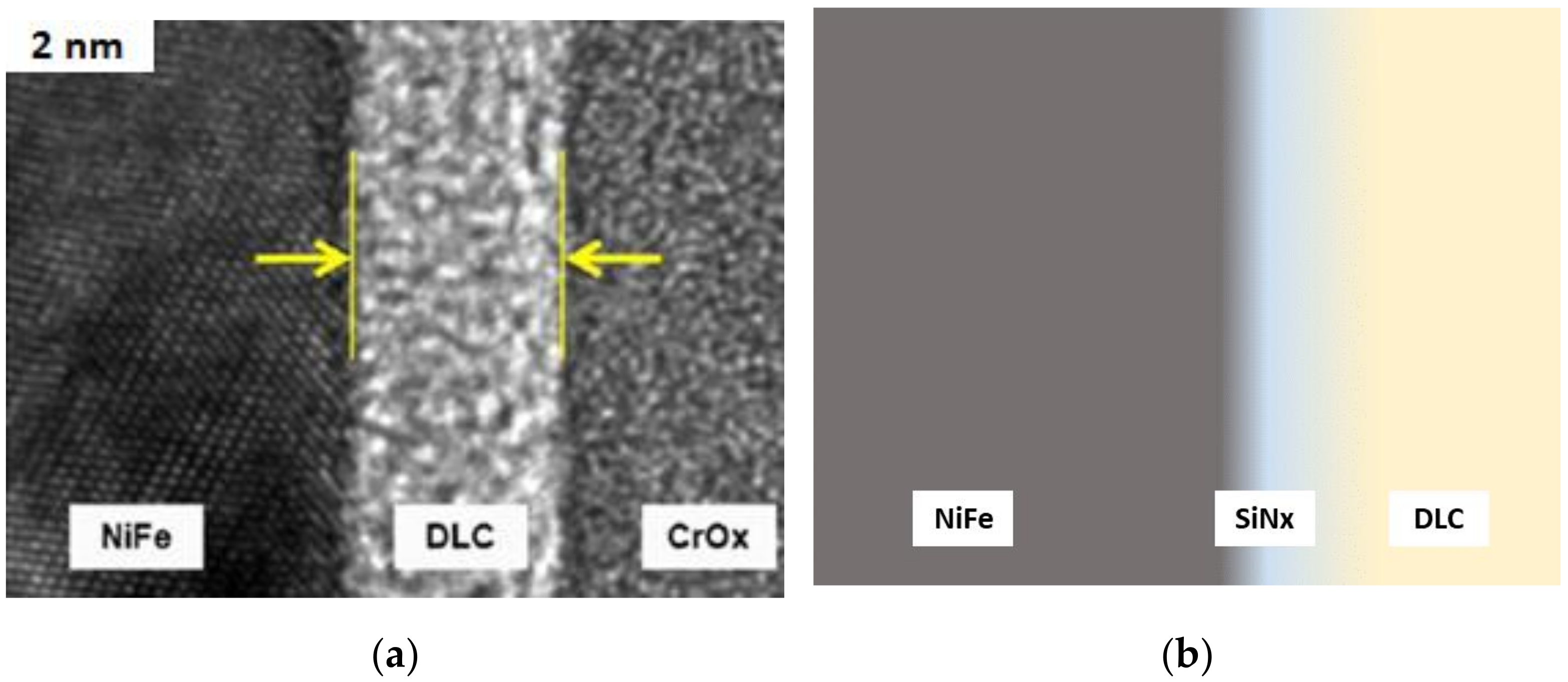
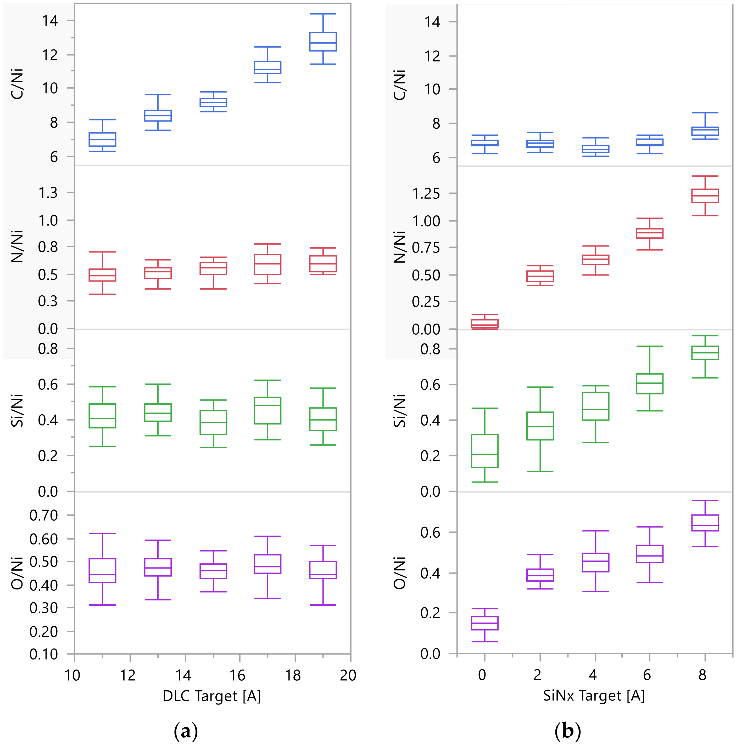
  • DLC thickness ladder: Film thicknesses were targeted within the 10–20 Å regime, with a 2 Å step size, forming a DLC thickness ladder. Prior to DLC deposition, a (fixed) 2 Å silicon nitride (seed) layer was reactively sputtered, i.e., Si target and nitrogen gas. Since the sputtered silicon nitride on that thickness scale is generally non-stoichiometric [27], we will refer to it as SiNx throughout the text.
  • Seed thickness ladder: The DLC thickness was fixed at the lowest target thickness used in the DLC ladder, whereas SiNx seed thickness was varied between 0 and 8 Å, with 2 Å step size.
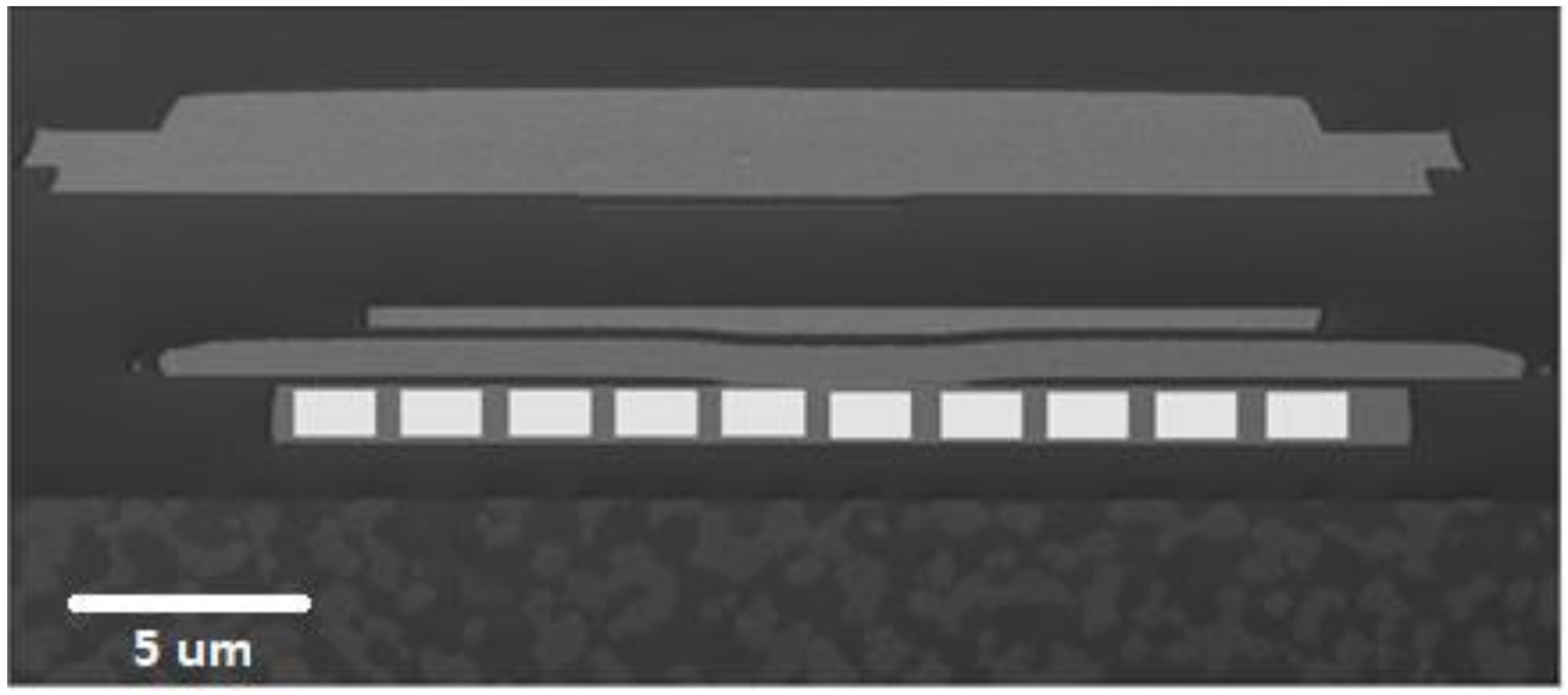
  • Films with a wider variation of total thickness: Additional films were produced with various DLC and SiNx levels, in order to enable a wide relative compositional range to enable thickness correlation between SEM/EDX and TEM. Film thicknesses, as measured by TEM, were varied between 10 and 30 Å, which at the higher end of thickness are up to 10 Å thicker than those of the ladder samples.
  • Films with varying oxygen contamination levels: In addition to DLC and SiNx, some depositions varied oxygen levels by intentionally varying the vacuum condition from 10−5 to 10−7 Torr—the higher the vacuum, the lower the oxygen partial pressure in the chamber. This was intended to demonstrate the sensitivity of the technique to oxygen detection.
A subset of the coated heads with a sufficiently large DLC stack compositional range was used in a metrology gauge repeatability and reproducibility (GR&R) capability study to assess the SEM/EDX characterization method in terms industry-level applications.

2.2. Analytical Methods

Atomic Force Microscopy (AFM) images of wear samples were acquired using a Park XE series AFM tool (Park Systems, Suwon, Korea) in non-contact mode. AFM scan was performed across the NiFe substrate with the aim at measuring the topography of DLC wear regions. Depth profiles were produced across wear areas and compared to those of SEM/EDX scans for the same areas.
SEM/EDX was performed on the NiFe substrate with various DLC film stacks using a Zeiss Merlin field emission gun (FEG) SEM (Carl Zeiss, Oberkochen, Germany) integrated with a windowless Oxford Ultim Extreme EDX system. For each head, 10 (1.5 × 1.0 µm2) separate maps were acquired along the NiFe substrate, as indicated in Figure 1. Multiple maps are acquired over the NiFe substrate to improve the statistics. The map sizes are generally defined to fit within the NiFe substrate. EDX experiments were conducted at 1.0 kV incident beam energy, 187 nA probe current, 5.0 mm working distance, and 20%–30% dead time. Maps were found to be more representative of each region analyzed compared to spot analysis, although either mode is acceptable. Summed EDX spectrum from each map was post-processed via a custom-made Python script that automatically extracts the data from the raw file (*.msa format) and removes the background for Si–L, C–K, N–K, O–K, Fe–L, and Ni–L characteristic X-ray peaks, as shown in Figure 2. The Python script was instrumental in keeping the data extraction constant as well as enabling high throughput analysis. Absolute peak amplitudes as well as amplitude ratio with Ni–L are automatically extracted, measured, calculated, and recorded. Ni–L, the major component of the NiFe substrate, was selected as a reference signal since, at 1.0 kV incident energy, the NiFe substrate can be treated as a semi-infinite substrate, and all the other X-rays of interest can be tracked and compared sample-to-sample in a semi-quantitative manner when taken their ratio to that of Ni–L in the substrate.
To provide Angstrom-level accuracy on the film thickness measurement, TEM high resolution imaging was performed using a Schottky FEG TEM (Thermo Fisher Scientific, Hillsboro, OR, USA) operating at 200 kV. TEM images, such as that shown in Figure 3a, were used to measure the DLC film thickness between NiFe substrate and a Cr2O3 added layer that protects the DLC film from the Focused Ion Beam (FIB) milling process during TEM lamellae preparation, as discussed extensively in [18]. The substrate, film and Cr2O3 stack is subjected to FIB milling and thinning, followed by extraction of the resulting TEM lamella and lift out on to a Cu grid. The cross-sections were performed at the NiFe substrate on sister heads of those undergone SEM/EDX, i.e., heads that underwent the same film deposition process and were arranged in close proximity in the deposition chamber. This arrangement helped prevent any minor contamination from the SEM/EDX process, as well as enabled parallel, efficient processing of the SEM/EDX and the TEM experiments. All films produced were also checked by EELS in the TEM for qualitative elemental assessment of the stack composition. A schematic drawing of the as-deposited SiNx/DLC layer stack on NiFe as seen by EELS, including a gradient effect representing intermixing between the various layers, is shown in Figure 3b, for clarity.

2.3. Wear Analysis

A subset of heads with the SiNx/DLC film stack was subjected to tribological wear stress tests [28] to generate wear tracks in a controlled manner, where the head flies on a disk with applied loads until DLC burnishing is detected via changes in read-write parametrics on a Guzik V2002 spin-stand tester (Guzik Technical Enterprises, Mountain View, CA, USA). The intent was to induce well-defined wear regions on the NiFe substrate that could be later characterized using combined AFM (Park Systems, Suwon, Korea) and SEM/EDX in terms of chemical changes associated to DLC and SiNx loss.

3. Results

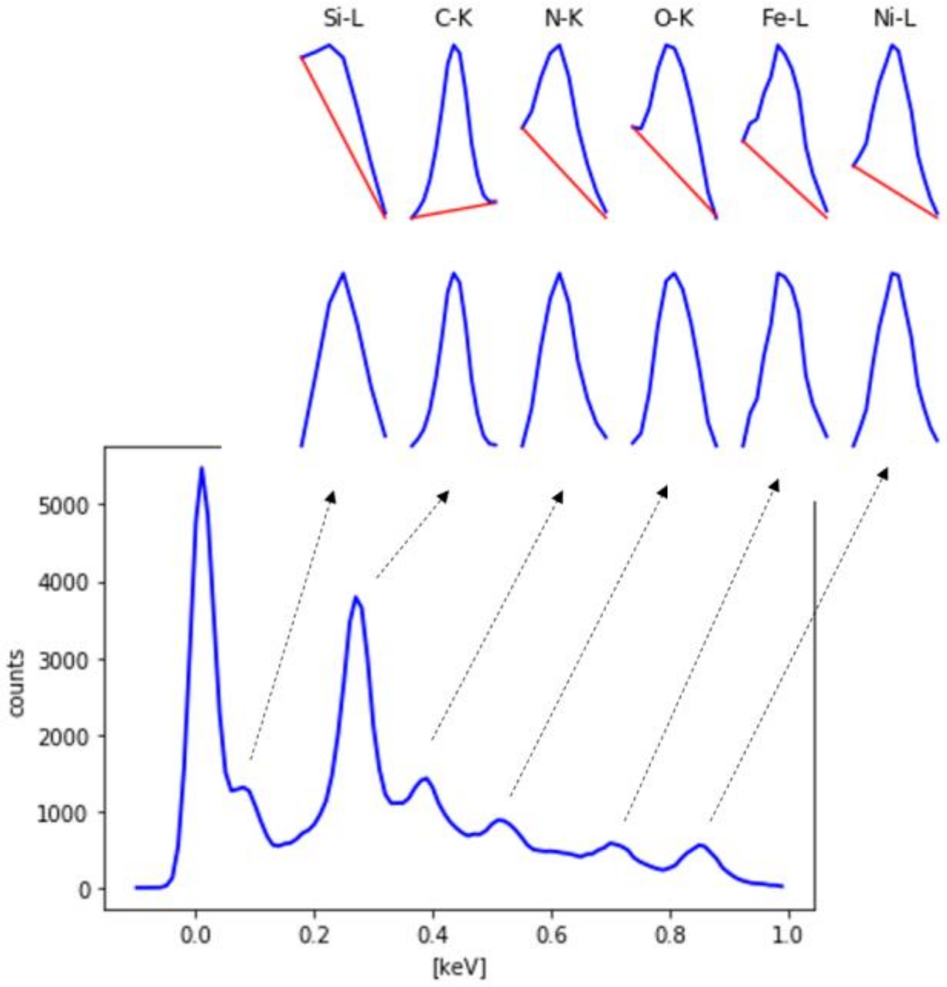
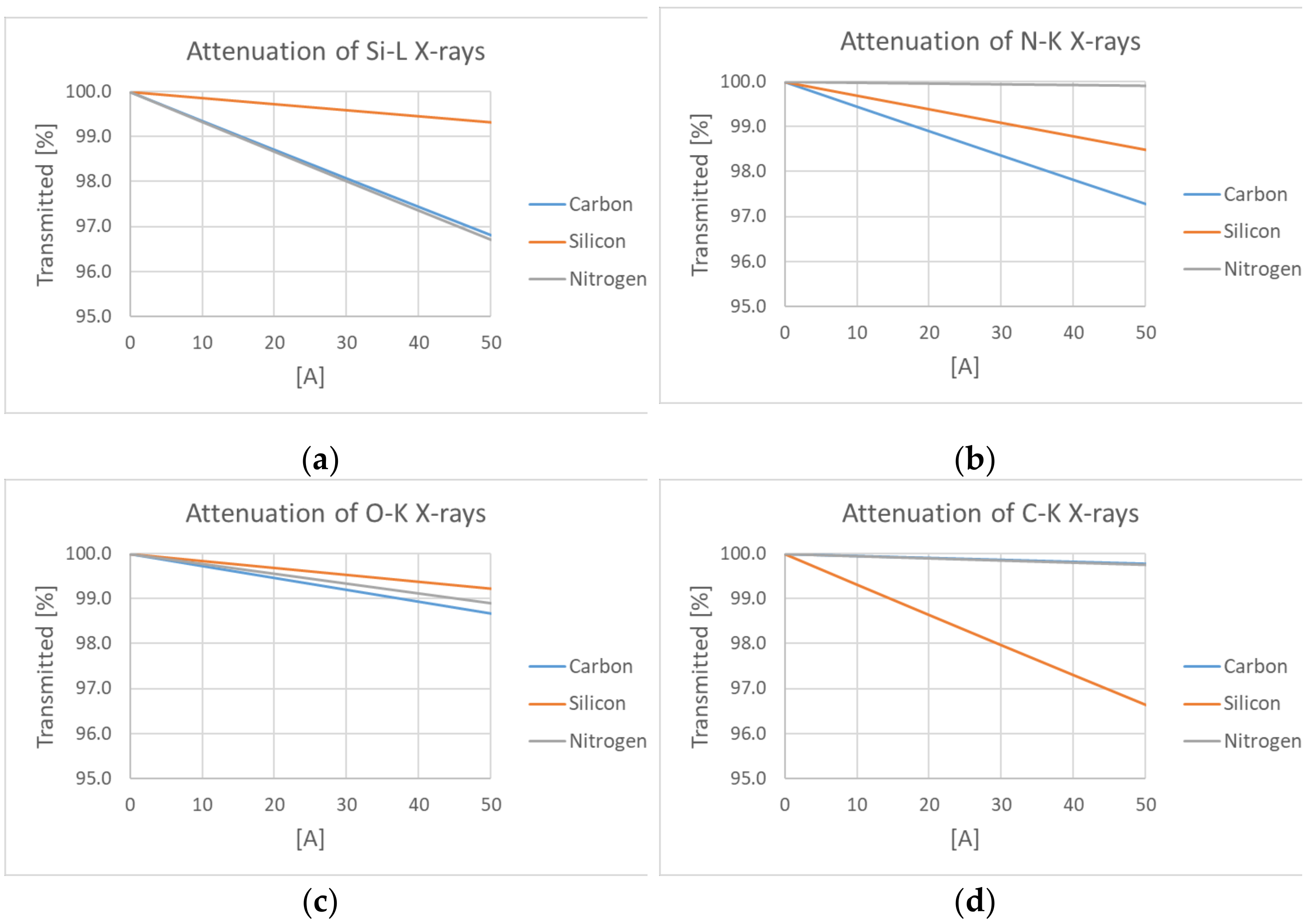
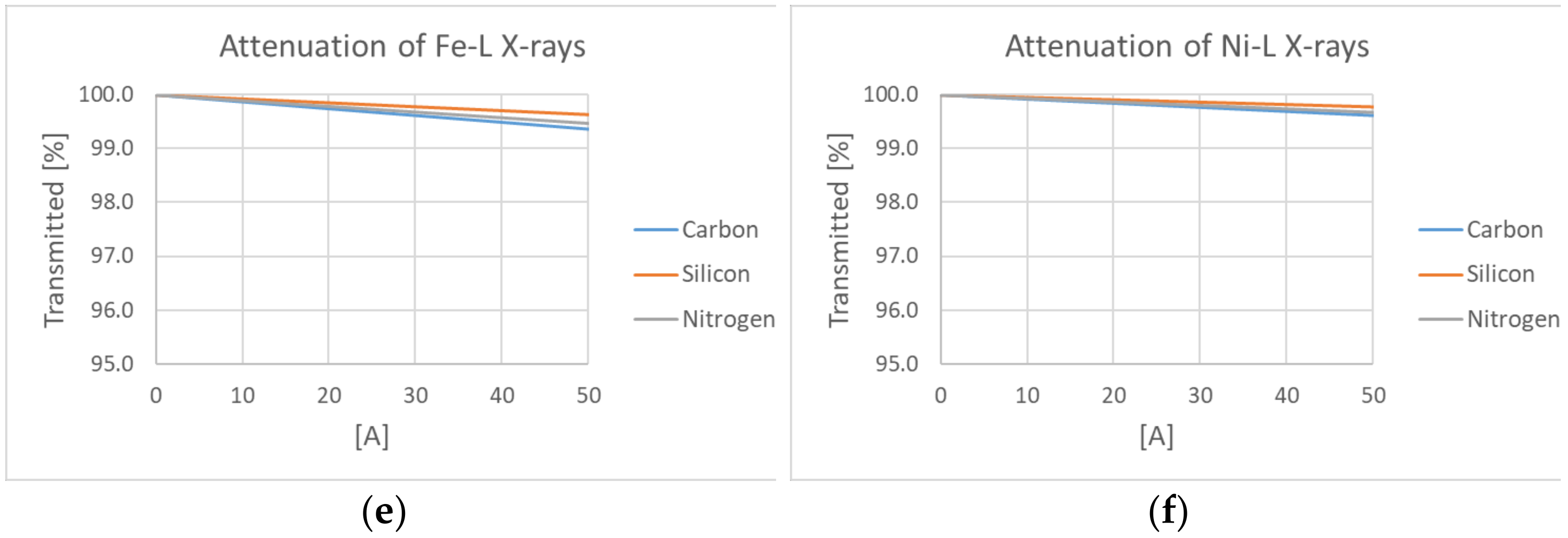
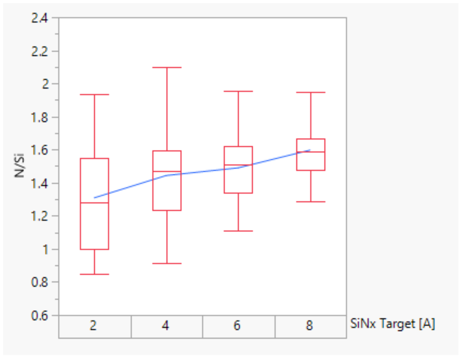
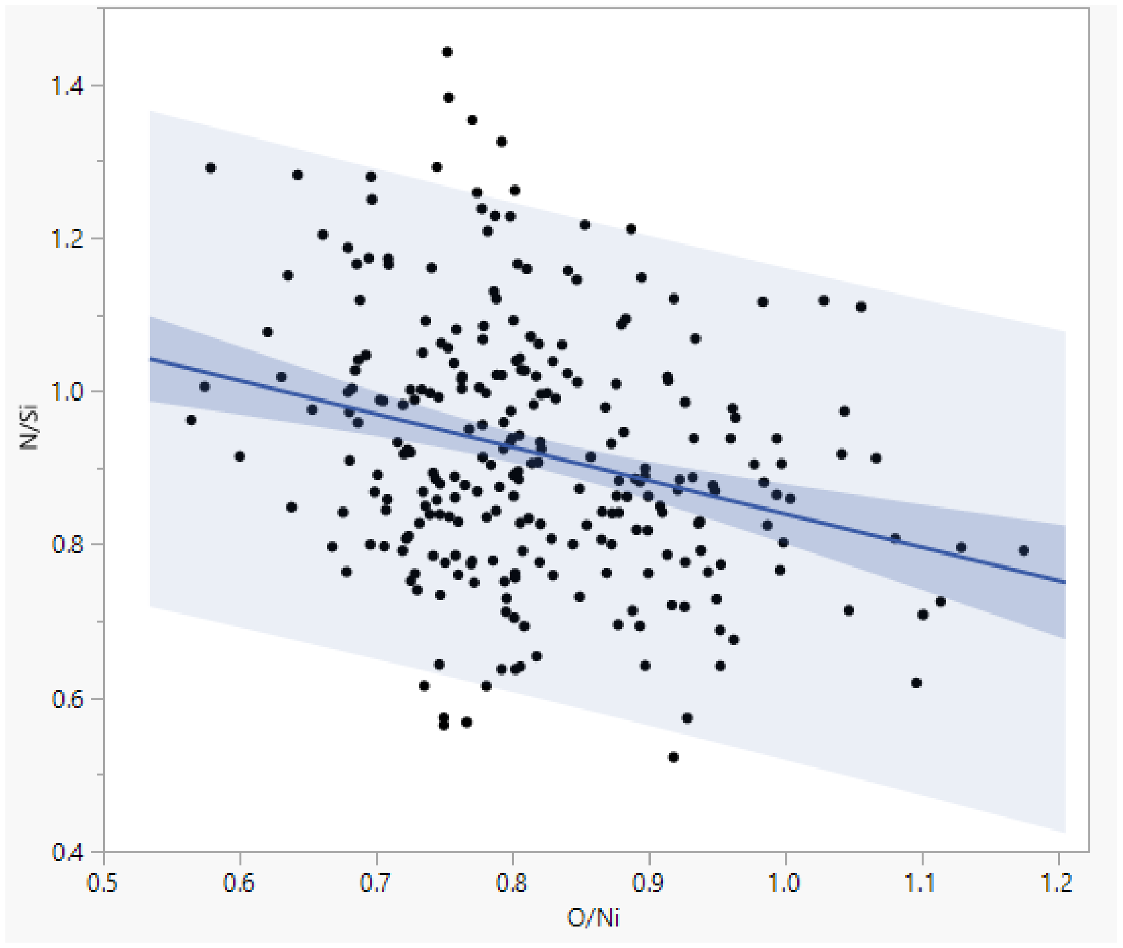
3.1. Compositional Sensitivity

Figure 4 shows EDX C/Ni, Si/Ni and N/Ni ratios as a function of deposited carbon for the DLC ladder, and of deposited SiNx for the seed ladder, both with 2 Å steps. It is clear that the SEM/EDX technique with the ratio (to Ni) method is sensitive to C, Si and N, producing a near-linear ratio increase with increasing amounts of deposited material. The data spread is higher for Si compared to C and N due to the fact that the Si–L peak is less pronounced and sits on the tail of the electronics noise peak of the EDX spectrum (Figure 2). The results also show that the C/Ni ratio increase in the DLC ladder, resulting from C deposition increments, and does not disturb the detection of N or Si, which remain roughly constant. Likewise, adding more SiNx in the seed ladder will only increase Si/Ni and N/Ni, but will not change C/Ni. This means that, within the thickness regime and seed/DLC compositions studied in this work, EDX Si/Ni, N/Ni, and C/Ni are independent functions of the actual amount of each element in the film.
Small variations on Si/Ni and/or N/Ni on the DLC ladder, or, conversely, of C/Ni on the seed ladder, are believed to be caused by subtle statistical variations on the deposition process at the Angstrom level, which can be expected for industrial scale processes. This effect also accounts for small deviations from linearity on the plots shown in Figure 4. Nevertheless, the intended step size was generally maintained constant between the ladder points. Although all depositions for the ladders shown in Figure 4 were performed with a fixed chamber pressure, the oxygen level (O/Ni) was found to increase with the SiNx ladder, whereas no significant oxygen change was observed on the DLC ladder. This result suggests that the SiNx functions as an oxygen getter, and that oxygen does not change DLC (and SiNx) detection by the EDX ratio method.

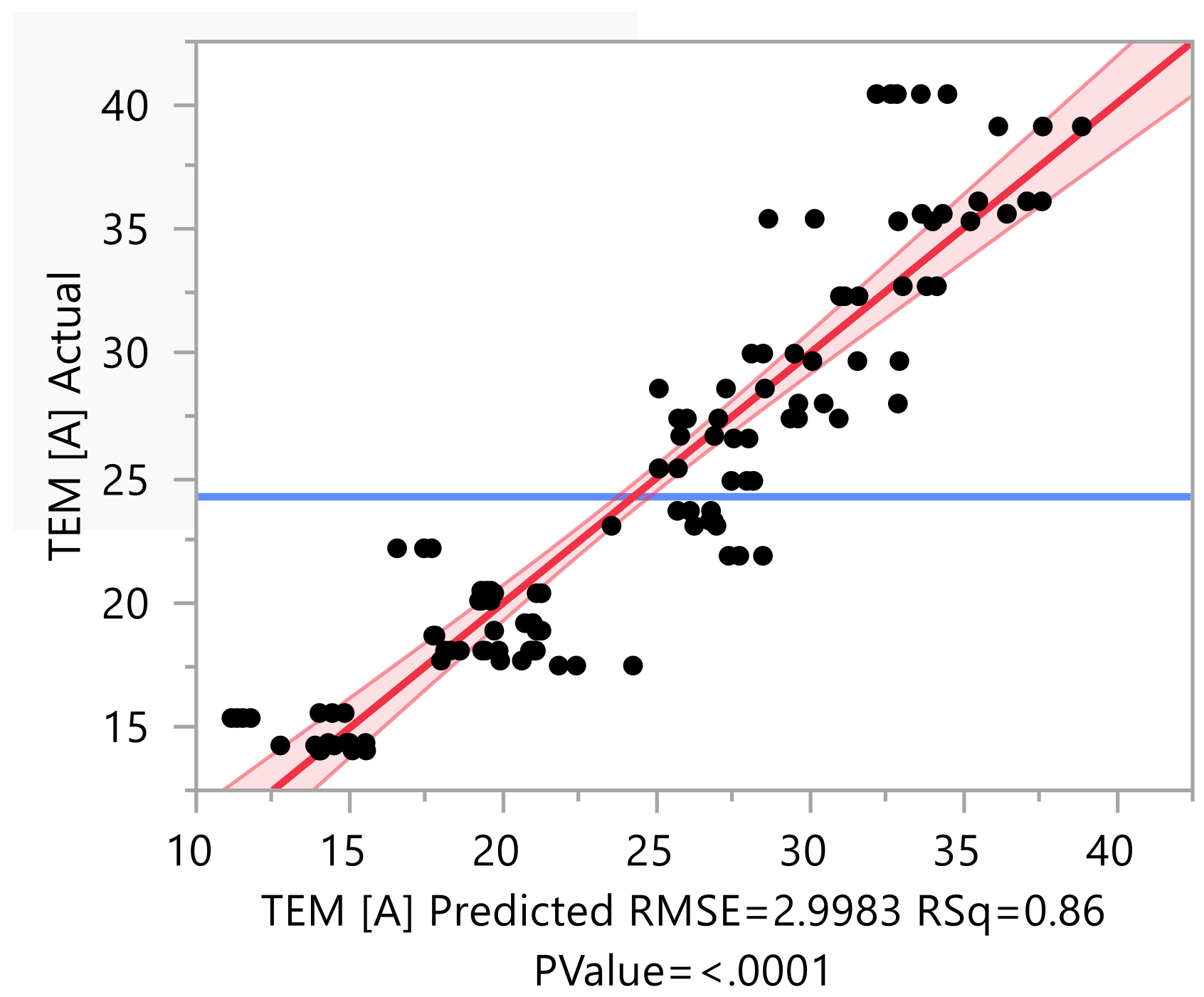
3.2. Thickness Model, Correlation with TEM, and Gauge Capability
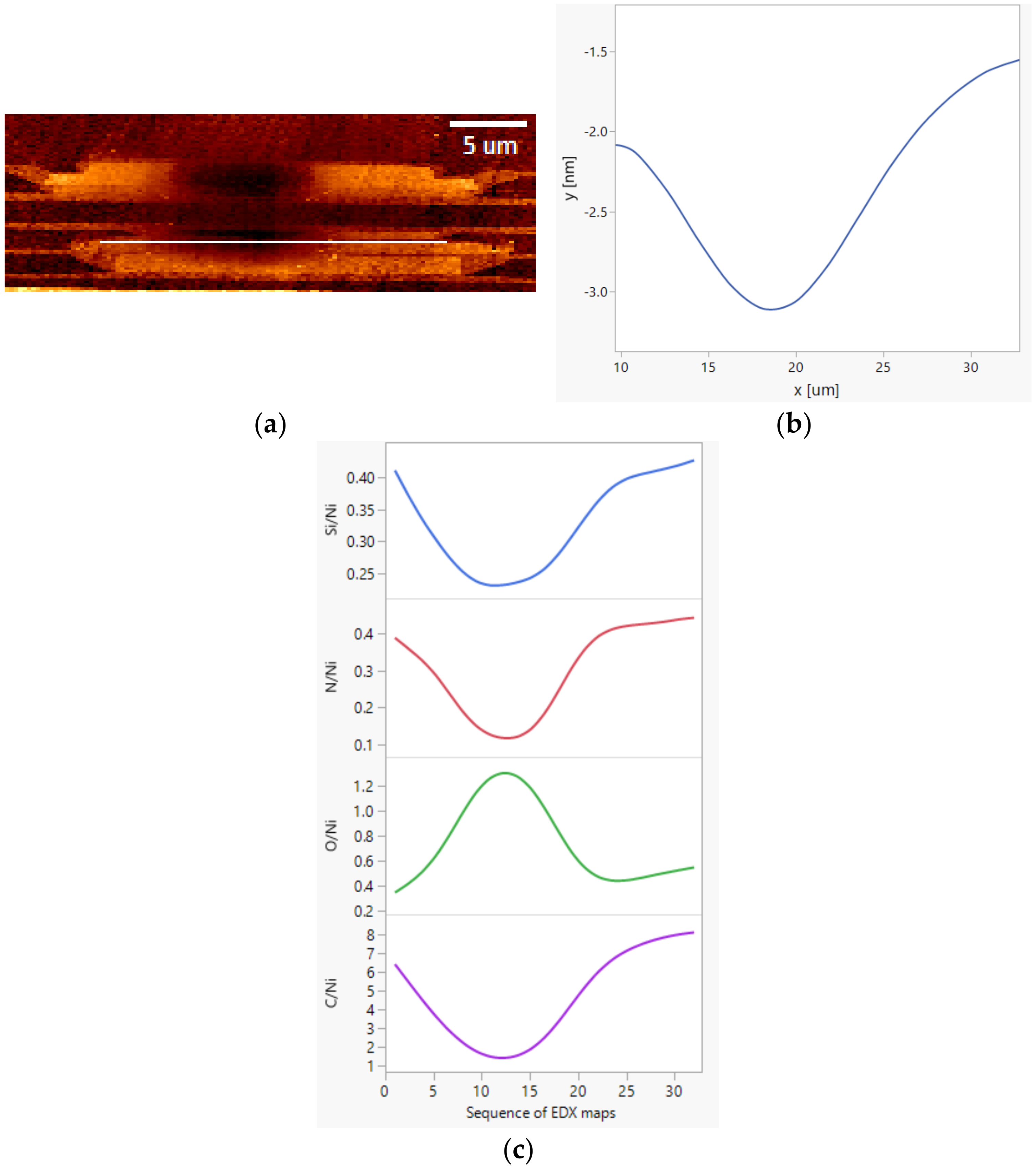
As observed in Figure 4, to a fair approximation, the DLC film thickness is a linear function of the amount of each of its constituents, i.e., C, Si, and N. Oxygen in the film and at the substrate/film interface is expected to cause thickness inflation due to the volume expansions involved in the formation of oxides, and thus, arguably, needs to be part of the thickness model as such. For example, silicon nitride is known to be thermodynamically unstable and tends to form a passivation SiNOx layer that prevents further oxidation to take place [29]. In order to predict the thickness as measured by TEM in Angstroms, one can take the EDX C, Si, N, and O ratios with Ni as independent variables on a multiple linear regression model with regression parameters a0, a1, a2, a3 and a4, as follows:
TEM   A = a 0 + a 1 C Ni + a 2 Si Ni + a 3 N Ni + a 4 O Ni ,
To build the Model, DLC films with varying Si, N, and C contents, as well as with varying O based on different vacuum levels during deposition, were analyzed by both SEM/EDX (ratios with Ni) and TEM (direct thickness measurement). The model prediction results are shown in Figure 5. Good predictability of TEM film thickness is demonstrated by acceptable p-value < 0.0001, relatively high Adjusted R-Square and low Root Mean Square Error (RMSE). The error can be assigned to small discrepancies between the two techniques. For example, the contrast change that defines the DLC thickness on a TEM image does not account for some of the seed layer material that was buried into the NiFe substrate. On the other hand, the SEM/EDX will detect the buried material, as well as potential pre-DLC inclusions or contaminants on the original surface, typically O, Si, and N. Moreover, some Si migrated to the surface forms a SiO2 mono-layer, and that layer may create additional surface roughness leading to some level of uncertainty in the TEM measurement [27].
Another source of error in the correlation is the natural variance in each of the two techniques. Table 1 shows a summary of the SEM/EDX gauge capability study using the ratio method. The intent is to define the gauge Sigma for each ratio for an intentionally broad range of film compositions (i.e., thicknesses) around industry-level thickness films, as well as repeated load-unload cycles for three distinct operators. The result shows that the statistical parameters involved in repeatability and reproducibility tests, i.e., % contribution, % GRR, and number of distinct categories (NDC), are within acceptable ranges for all four ratios, meaning that differentiation of the various categories or films is achieved. Carbon has the best GR&R overall, followed by nitrogen. Oxygen and silicon are within acceptable levels. The Sigma values shown in Table 1 can be directly utilized to infer whether or not a certain ratio delta for any measured pair of ratios, for instance C/Ni for two subsequent depositions of the same kind, is statistically significant from a metrology standpoint.

3.3. Wear Analysis

AFM topographic scan of a magnetic head over the reader-writer block (Figure 6a) reveals recessed regions at NiFe substrate. The corresponding depth profile is shown in Figure 6b, where a recession of ~10 Å can be measured on the NiFe substrate. This head was submitted to wear stress tests, and the recessed regions were subsequently confirmed (by TEM) to be a manifestation of DLC wear. SEM/EDX acquired along the reader shield corroborates with the DLC wear hypothesis, as the wear regions were found to correspond to decreased C, Si, and N, and increased O, as shown in Figure 6c. The increase in oxygen is primarily connected to FeOx formation at the partially or fully unprotected NiFe substrate. Significant depletion in both Si and N reveals that the wear was sufficiently deep to remove both DLC and silicon nitride materials.
The thickness loss at the most recessed areas of the NiFe substrate with respect to the baseline, un-recessed areas can be estimated directly by plugging in the EDX C/Ni, Si/Ni, N/Ni, and O/Ni ratios from those two regions in Equation (1), corresponding to ~7 Å. This value is comparable to the AFM topographic profile in Figure 6b, and further validates the SEM/EDX approach. However, the calculated film thickness in this case will be slightly over-estimated by the oxygen originated from FeOx, and not manifested by the original film itself. In the experiment in Figure 6, assuming that all oxygen signal comes from FeOx, and that C, Si, and N are fully consumed by the wear event, then plugging the O/Ni ratio in Equation (1) yields a TEM thickness of ~2 Å, which can be assumed as the maximum error due to excess (i.e., newly formed FeOx) oxygen present at the wear area.

4. Discussion

It was observed that, for the ultra-thin DLC film stacks studied, Si/Ni and N/Ni ratios are independent of carbon increments in the DLC ladder, and C/Ni ratio is independent of both Si and N increments in the seed ladder. This result indicates that the EDX ratio method does not require deconvolution of X-ray attenuation effects for each material layer within the film, as would be expected for thicker film quantification models [25]. In order to further investigate and quantify the extent to which X-ray attenuation effects can be disregarded, as well as to verify whether the same applies for oxygen, ab-initio calculations were performed using the Beer-Lambert law of attenuation [30]:
I = I 0 · e μ x ,
where I is the intensity of photons transmitted across some distance travelled x (for example the film thickness itself), I0 is the initial intensity of photons, and µ is the linear attenuation coefficient of that photon through that medium. Using the mass attenuation coefficients for Si–L, C–K, N–K, O–K, Fe–L, and Ni–L X-ray photons from [31] and multiplying by the density of each element, it is possible to calculate the linear attenuation coefficient for each type of X-ray photon of that element constituent of the DLC stack layer. The plots shown in Figure 7 correspond to the attenuation of each X-ray photon detected by the SEM/EDX method on the C (DLC), and on the Si and N portions of the SiNx layer (here assumed to be stoichiometric Si3N4). It is demonstrated that the transmittance of all the X-ray photons of interest is above 98% for the practical range of thicknesses used in industrial DLC film stacks, thus corroborating the empirical results presented in Section 3.1, as well as those of the thickness model in Section 3.2, since each ratio can be treated separately in the transfer function. This reinforces that the SEM/EDX ratio method can be used as a direct, semi-quantitative metric of material concentration, without the need to account for interactions between all the different materials present in the film, the same being true for oxygen. The Fe–L photon was deliberately added in this analysis only for completeness, since attenuation of Fe–L X-rays would not play any role in the method i.e., ratio with Ni–L is important, and not with Fe–L. From all the X-ray photons and film materials of interest, the following interactions were found to be the strongest: Si–L and C–K on SiNx, and N–L on DLC. The effect of these interactions can be ignored.
The fact that linearity is maintained in the plots shown in Figure 4 confirms that the incident electron beam is penetrating through both SiNx-DLC film and NiFe substrate. When electron beam-film interaction starts to supersede that of electron beam-substrate, the ratio of X-ray photons from materials in the film to those of Ni (substrate) is expected to depart from linearity with respect to film thickness. The ratio between DLC stack X-ray photons and Ni–L will increase exponentially as Ni–L X-ray counts will drop likewise. That threshold thickness is estimated to be around 100 Å depending on how much SiNx is present in the stack and/or intermixed with carbon and is significantly larger than that of ultra-thin DLC used in the HDD industry today. While in the linear regime of EDX ratio increase with film deposition, direct inferences between any two films/elements can be made based on relative proportions between the ratios of the same element to Ni–L in the films. An important consequence is that the SEM/EDX ratios can be used as film quality control in industrial assembly lines, with near-Angstrom precision of projected, modeled thickness. Modeled thickness Sigma estimates can be calculated from Equation (1) using the GR&R Sigma for each element ratio with Ni, while keeping the other elements fixed, i.e., 0.2 Å for C, 0.7 Å for Si, 0.8 Å for N, and 0.1 Å for O. Statistical process control charts with control limits around each element of interest, as represented by its ratio with a substrate element, can be established and monitored appropriately. One particular interaction of relevance is the effect of N/Si ratio on the strength of the SiNx layer (i.e., the closer it gets to stoichiometric Si3N4), which has been postulated to control diffusional phenomena through ultra-thin DLC films used in the HDD industry [27]. In the present study, it is demonstrated that the N/Si ratio can be conveniently monitored. In the seed ladder, the N/Si ratio increases with the SiNx content, as shown in Figure 8. The N/Si ratio obtained by the SEM/EDX technique at low kV is not calibrated with a standard, and does not reflect the actual atomic percent ratio. However, it can be used as a relative comparison (i.e., higher vs. lower N/Si ratio) for different film stacks.
For a fixed chamber pressure, it was found that oxygen levels increase with the SiNx deposition due to the SiNx ability to retain oxygen. Another interesting insight the SEM/EDX technique provides is that, from the DLC film depositions in which oxygen was intentionally varied, the presence of oxygen in the film seems to inhibit N/Si ratio increases for higher levels of oxygen, as shown by the generally marginal inverse correlation shown in Figure 9 for O/Ni < ~0.9. However, the data is too scattered to make this a strong prediction, particularly for lower levels of oxygen. Conversely, it is expected that higher N/Si ratios will yield thicker films due to lack of intermixing/interaction between SiNx and substrate and DLC.
Both oxidation and strong (more stoichiometric) SiNx films tend to inflate the DLC thickness, and both effects are automatically accounted for in the model (Figure 4). The interaction between the two factors is represented mathematically via the regression parameter, i.e., positive for N/Ni, and negative for both Si/Ni and O/Ni, indicating a compensating mechanism to avoid all three contributions to over-estimate the TEM thickness by either the presence of both O and SiNx, or by the formation of a stronger SiNx layer. Following the same rationale, two additional, more compact models can be postulated, one where oxygen can be omitted from the original model shown in Equation (1) (Equation (3)), and the other where O/Ni is maintained, but Si/Ni and N/Ni are replaced with the N/Si ratio (Equation (4)):
TEM   A = a 0 + a 1 C Ni + a 2 Si Ni + a 3 N Ni ,
TEM   A = a 0 + a 1 C Ni + a 2 O Ni + a 3 N Si .
Thickness prediction results for both models are shown in Figure 10. The N/Si model in Equation (4) is better than both the more generalized equation in Equation (1) and the model that omits oxygen, Equation (3). Removing the oxygen from Equation (1), leading to Equation (3), does not change the prediction metrics significantly. The compensating mechanism between N/Si ratio and O in Equation (4) is thus confirmed by the ability of that model to predict TEM thickness slightly better than the generic model in Equation (1).
Generalizations can be made of the SEM/EDX ratio method. Film stack compositions for which distinctive, characteristic X-ray peaks are produced at low kVs, as well as for which a given substrate element also produces a viable X-ray event, and for which attenuation of all those X-ray photons by the layers/phases in the film can be either measured or calculated using the methodology described hereto, and ignored, are potential candidates for undergoing the same simplifications leading to the ratio method. An example is DLC with varying densities [19], which would lead to only marginal changes in the calculation of photon attenuation by the carbon layer, i.e., Si–L attenuation change would be within 1.1%, N–K 0.9%, and O–K 0.5%, assuming the carbon layer changes dramatically from graphite (2.25 g/cm3) to diamond (3.50 g/cm3). Another interesting case in the HDD industry would be DLC film characterization on media platter. On a nanometer scale, media surfaces have grains [32] protruding perpendicularly to the plane of the platter, and thus TEM characterization is challenged due to poor edge on condition between DLC and the substrate. One possible solution is to apply the SEM/EDX technique, as long as media DLC is sufficiently thin (i.e., comparable to that of heads) and that the complex substrate systems are stable and have at least one element present that can be used as semi-infinite component.
Correlative techniques such as AFM and SEM/EDX are also possible in the context of the DLC characterization method presented in this work. The power of effortlessly describing the chemistry of an AFM-detected, wear-like damage using SEM/EDX, was clearly demonstrated in Section 3.3. Additional insights to the technique can be correlatively produced with Conductive Atomic Force Microscopy (CAFM). In [33] it was revealed that the DLC film causes the surface to be conductive, and that conductivity would vary with the oxidation of the SiNx layer as well as with the DLC thickness, as revealed by TEM/EELS. Using the SEM/EDX technique would provide the same understanding, without the sampling constraints and complexity of TEM x-sections. A step further follows the work by [34], where SEM image contrast at low kV is calibrated with AFM depth profiles as the DLC (a low electron yielding elemental composition) is removed from the head NiFe substrate’s surface (i.e., a higher electron yielding elemental composition), providing a simulated depth profile with a SEM image instead of an AFM scan. In conjunction with the SEM/EDX ratio method, it is possible to add a new layer of comprehension with stack layer elemental analysis being directly correlated to AFM topography and/or SEM image contrast and/or CAFM maps, i.e., a robust, higher throughput replacement for TEM/EELS analysis of the film.

5. Conclusions

This work described a novel method of characterizing ultra-thin diamond-like films on actual HDD head functional substrate using SEM/EDX, which is a relatively simple, high throughput analytical technique. Since the attenuation of X-rays that participate in the ratio method between DLC film stack and substrate material is negligible and can be ignored, important simplifications lead to the film thickness description as a linear, independent function of each of its components, without the need to deconvolute X-ray/film interactions. Three thickness correlation models with TEM were postulated, achieving reasonably high predictive metrics and an error of a few Angstroms or less. The SEM/EDX ratio method technique also revealed a complex interplay between oxygen and N/Si ratio in the seed layer, where the N/Si ratio will decrease very slightly with higher deposition chamber pressures, and instead will increase significantly for a fixed chamber pressure and varying SiNx thicknesses. The gauge repeatability Sigma achieved was 0.2 Å for C, 0.7 Å for Si, 0.8 Å for N, and 0.1 Å for O. Wear track depth measured by AFM was ~10 Å, which is close enough to the ~7 Å measured by the SEM/EDX technique also taking into consideration a possible 2 Å FeOx layer formed on the NiFe substrate.

Author Contributions

Conceptualization and writing, original draft preparation, G.P.S.; writing review and overall technical review and advising, K.C.R.; experimental work, C.P.; academic supervision of C.P. and technical advising, K.C.; All authors have read and agreed to the published version of the manuscript.

Funding

This research received no external funding.

Institutional Review Board Statement

Not applicable.

Informed Consent Statement

Not applicable.

Data Availability Statement

Data is contained within the article.

Acknowledgments

The authors acknowledge Mongkhol Suwanno and Budi Suswadi for providing the samples used in this study, Nutthavin Thongpitithanawat for the TEM sample preparation, Bram Cantaert and Nicholas Vito for the EELS analysis, Sanpon Vantasin for the AFM analysis, and Sit Kerdsongpanya for coordinating sample logistics.

Conflicts of Interest

The authors declare no conflict of interest.

References

  1. Bogy, D.B.; Yun, X.H.; Knapp, B.J. Enhancement of head-disk interface durability by use of diamond like carbon overcoats on the slider’s rails. IEEE Trans. Magn. 1994, 30, 369–374. [Google Scholar] [CrossRef]
  2. Yasui, N.; Inaba, H.; Furusawa, K.; Saito, M.; Ohtake, N. Characterization of head overcoat for 1 Tb/In2 magnetic recording. IEEE Trans. Magn. 2009, 45, 805–809. [Google Scholar] [CrossRef]
  3. Avalos-Borja, M.; Hirata, G.A.; Contreras, O.; Ning, X.G.; Duarte-Moller, A.; Barna, A. TEM and PEELS characterization of diamond films grown on Si substrates. Diam. Relat. Mater. 1996, 5, 1249–1253. [Google Scholar] [CrossRef]
  4. Yan, X.; Tao, X.; Chen, G.; Yang, S.; Liu, H. Study of structure, tribological properties and growth mechanism of DLC and nitrogen-doped DLC films deposited by electrochemical technique. Appl. Surf. Sci. 2004, 48, 2665–2681. [Google Scholar] [CrossRef]
  5. Gayathri, S.; Kumar, N.; Krishnan, R.; Ravindran, T.; Dash, S.; Tyagi, A.; Raj, B.; Sridharan, M. Tribological properties of pulsed laser deposited DLC/TM (TM = Cr, Ag, Ti, and Ni) multilayers. Tribol. Int. 2012, 53, 87–97. [Google Scholar] [CrossRef]
  6. Nöthe, M.; Breuer, U.; Koch, F.; Penkalla, H.; Rehbach, W.; Bolt, H. Investigation of the structure and properties of a-C:H coatings with metal and silicon containing inter layers. Appl. Surf. Sci. 2001, 179, 122–128. [Google Scholar] [CrossRef]
  7. Wei, C.; Wang, Y.S.; Tai, F.C. The role of metal interlayer on thermal stress. Film structure, wettability and hydrogen content for diamond like carbon films on different substrate. Diam. Relat. Mater. 2009, 18, 407–412. [Google Scholar] [CrossRef]
  8. Cui, Y.X.; Shen, B.; Sun, F.H. Influence of amorphous ceramic interlayers on tribological properties of CVD diamond films. Appl. Surf. Sci. 2014, 313, 918–925. [Google Scholar] [CrossRef]
  9. Polini, R.; Barletta, M. On the use of CrN/Cr and CrN interlayers in hot filament chemical vapour deposition (HF-CVD) of diamond films onto WC–Co substrates. Diam. Relat. Mater. 2008, 17, 325–335. [Google Scholar] [CrossRef] [Green Version]
  10. Endler, I.; Leonhardt, A.; Scheibe, H.J.; Born, R. Interlayers for diamond deposition on tool materials. Diam. Relat. Mater. 1996, 5, 299–303. [Google Scholar] [CrossRef]
  11. Li, Y.; Tang, Y.; Yang, Q.; Xiao, C.; Hirose, A. Growth and adhesion failure of diamond thin films deposited on stainless steel with ultra-thin dual metal interlayers. Appl. Surf. Sci. 2010, 256, 7653–7657. [Google Scholar] [CrossRef]
  12. Dwivedi, N.; Rismani-Yazdi, E.; Yeo, R.J.; Goohpattader, P.S.; Satyanarayana, N.; Srinivasan, N.; Druz, B.; Tripathy, S.; Bhatia, C. Probing the role of an atomically thin SiNx interlayer on the structure of ultrathin carbon films. Sci. Rep. 2014, 4, 1–10. [Google Scholar] [CrossRef] [PubMed] [Green Version]
  13. Chen, Q.; Shih, K.; Shen, Y.; Luo, Y.; Li, R. Effects of SiNx interlayer on characterization of amorphous diamond-like carbon films. Mater. Sci. Technol. 2015, 31, 703–708. [Google Scholar] [CrossRef]
  14. Shahsavari, F.; Ehteshamzadeh, M.; Naimi-Jamal, M.R.; Irannejad, A. Nanoindentation and nanoscratch behaviors of DLC films growth on different thickness of Cr nanolayers. Diam. Relat. Mater. 2016, 70, 76–82. [Google Scholar] [CrossRef]
  15. Wienss, A.; Persch-Schuy, G.; Hartmann, R.; Joeris, P.; Hartmann, H. Subnanometer scale tribological properties of nitrogen containing carbon coatings used in magnetic storage devices. J. Vac. Sci. Technol. A 2003, 18, 2023–2026. [Google Scholar] [CrossRef]
  16. Wienss, A.; Persch-Schuy, G.; Hartmann, R.; Joeris, P.; Hartmann, H. Scratching resistance of diamond-like carbon coatings in the subnanometer regime. Appl. Phys. Lett. 1999, 75, 1077. [Google Scholar] [CrossRef]
  17. Li, Y.; Yan, X.; Wei, J.; Zhang, G.; Feng, H.; Chen, Y.; Xie, Y. Dependence of optimum thickness of ultrathin diamond-like carbon coatings over carbon nanotubes on geometric field enhancement factor. ACS Appl. Electron. Mater. 2020, 2, 84–92. [Google Scholar] [CrossRef] [Green Version]
  18. Souza, G.P.; Ruthe, K.C.; Chen, L.; Hong, L.; Wang, H. Materials selection for ultra-thin diamond-like carbon film metrology and structural characterization by TEM. Microsc. Microanal. 2015, 21, 827–828. [Google Scholar] [CrossRef] [Green Version]
  19. Galvana, D.; Peia, P.Y.; Hossona, D.M.J.T.; Cavaleiro, A. Determination of the sp3 C content of a-C films through EELS analysis in the TEM. Surf. Coat. Technol. 2005, 200, 739–743. [Google Scholar] [CrossRef] [Green Version]
  20. Zhoa, J.M.; Yang, P. A method for determining ultrathin DLC film thickness by spectroscopic ellipsometry. Microsyst. Technol. 2012, 18, 1455–1461. [Google Scholar] [CrossRef]
  21. Jiang, Z.C.; Li, S.D.; Kam, Y.K.; Liu, Y.W. Method of Nano Thin Film Thickness Measurement by Auger Electron Spectroscopy. U.S. Patent No. U.S. 7,582,868 B2, 1 September 2009. [Google Scholar]
  22. Kumari, K.; Banerjee, S.; Chini, T.K.; Ray, N.R. Preparation of diamond like carbon thin film on stainless steel and its SEM characterization. Mater. Sci. 2009, 31, 563–567. [Google Scholar] [CrossRef]
  23. Safari, R.; Sohbatzadeh, F.; Mohsenpour, T. Optical and electrical properties of N-DLC films deposited by atmospheric pressure DBD plasma: Effect of deposition time. Surf. Interfaces 2020, 21, 100795. [Google Scholar] [CrossRef]
  24. Burgess, S.; Sagar, J.; Holland, J.; Li, S.; Bauer, F. Ultra-Low kV EDS—A new approach to improved spatial resolution, surface sensitivity, and light element compositional imaging and analysis in the SEM. Microsc. Today 2017, 25, 20–29. [Google Scholar] [CrossRef] [Green Version]
  25. Goldstein, J.I.; Newbury, D.E.; Michael, J.R.; Ritchie, N.W.; Scott, J.H.J.; Joy, D.C. Scanning Electron Microscopy and X-ray Microanalysis, 2nd ed.; Plenum: New York, NY, USA, 1992; pp. 69–84. [Google Scholar]
  26. Robertson, J. Diamond-like amorphous carbon. Mater. Sci. Eng. 2002, 37, 129. [Google Scholar] [CrossRef] [Green Version]
  27. Souza, G.P.; Ruthe, K.C.; Leary, S.P. Si diffusion in ultra-thin tetrahedral amorphous diamond-like carbon. In Proceedings of the 19th International Microscopy Congress (IMC 19), Sydney, Australia, 9–14 September 2018; p. 1345. [Google Scholar]
  28. Wallash, A.; Zhu, H.; Chen, D. A dynamic scratch test to study read/write head degradation due to head-disk interactions. IEEE Trans. Magn. 2008, 44, 3629–3632. [Google Scholar] [CrossRef]
  29. Riley, F.L. Silicon Nitride and Related Materials. J. Am. Ceram. Soc. 2000, 83, 245–265. [Google Scholar] [CrossRef]
  30. Swinehart, D.F. The beer-lambert law. J. Chem. Educ. 1962, 39, 333–335. [Google Scholar] [CrossRef]
  31. Henke, B.L.; Gullikson, E.M.; Davis, J.C. X-ray interactions: Photoabsorption, scattering, transmission, and reflection at E = 50–30,000 eV, Z = 1–92. At. Data Nucl. Data Tables 1993, 54, 181–342. [Google Scholar] [CrossRef] [Green Version]
  32. Piramanayagam, S.N. Perpendicular recording media for hard disk drives. J. App. Phys. 2007, 102, 011301. [Google Scholar] [CrossRef]
  33. Mejia, S.; Leary, S.P.; Souza, G.P.; Ruthe, K.C. Conductive atomic force microscopy characterization of ultra-thin diamond-like carbon films on magnetic recording heads. Microsc. Microanal. 2015, 21, 1613. [Google Scholar] [CrossRef] [Green Version]
  34. Leary, S.P.; Ruthe, K.C. Detecting Thickness Variation and Quantitative Depth Utilizing Scanning Electron Microscopy with a Surface Profiler. U.S. Patent 20160265908, 15 September 2016. [Google Scholar]
Figure 1. SEM back-scattering contrast image of reader and writer blocks, showing the NiFe substrate and, schematically, the location of the 10 (1.5 × 1.0 µm2) EDX maps. The ultra-thin DLC film growth direction upon deposition is perpendicular to the plane of the image.
Coatings 11 00729 g001
Figure 2. Example of a summed EDX spectrum for a single acquisition location, or map, and of peak post-processing output from a custom-made Python script that automatically extracts the data from the raw file and removes the background for Si–L, C–K, N–K, O–K, Fe–L, and Ni–L characteristic X-ray peaks.
Coatings 11 00729 g002
Figure 3. TEM image showing the DLC film sandwiched by the NiFe substrate and a Cr2O3 added layer that protects the DLC film from the Focused Ion Beam (FIB) milling process during TEM lamellae preparation (a). A schematic drawing of the as-deposited SiNx/DLC layer stack on NiFe is shown in (b).
Coatings 11 00729 g003
Figure 4. EDX C/Ni, Si/Ni, N/Ni and O/Ni ratios as a function of deposited carbon for the DLC ladder (a), and of the deposited SiNx for the seed ladder (b), both with 2 Å steps.
Coatings 11 00729 g004
Figure 5. Model prediction results for Equation (1), with parameters: a0 = 23.68; a1 = 0.86; a2 = −19.31; a3 = 19.00; a4 = −2.42.
Coatings 11 00729 g005
Figure 6. AFM topographic scan of a magnetic head over the reader-writer block (a) reveals recessed regions at the NiFe substrate. The corresponding depth profile on the NiFe substrate (b) corresponds to decreased C, Si and N, and increased O, as measured by the SEM/EDX technique (c).
Coatings 11 00729 g006
Figure 7. Attenuation of Si–L (a), N–K (b), O–K (c), C–K (d), Fe–L (e) and Ni–L (f) X-ray photons detected by the SEM/EDX method on the C (DLC), and on the Si and N potions of the SiNx (Si3N4) layer.
Coatings 11 00729 g007aCoatings 11 00729 g007b
Figure 8. SEM/EDX N/Si ratio as a function of SiNx content in the SiNx ladder.
Coatings 11 00729 g008
Figure 9. Oxygen level in the various films produced with intentionally varying oxygen levels in the deposition chamber reveal a slight tendency to inhibit N/Si ratio increase, differently from the SiNx ladder with a fixed chamber pressure experiment. However, the data is too scattered to make this a strong prediction, particularly for lower levels of oxygen (O/Ni < ~0.9).
Coatings 11 00729 g009
Figure 10. Model prediction results for Equation (3) (a), with parameters: a0 = 23.17; a1 = 0.86; a2 = −19.90; a3 = 18.03; and for Equation (4) (b), with parameters: a0 = 10.32; a1 = 1.52; a2 = −7.64; a3 = 10.09.
Coatings 11 00729 g010
Table 1. Gauge Repeatability and Reproducibility (GR&R) results for C/Ni, N/Ni, Si/Ni and O/Ni ratios.
ParameterC/NiN/NiSi/NiO/NiAcceptable Criteria
Total GR&R Sigma0.2600.0420.0340.045-
Contribution [%]0.492.107.125.17<7.7
GRR [%]6.9914.4926.6823.90<30
Number of Distinct Categories20955≥5
Publisher’s Note: MDPI stays neutral with regard to jurisdictional claims in published maps and institutional affiliations.

