Effects of Drying Temperature and Molar Concentration on Structural, Optical, and Electrical Properties of β-Ga2O3 Thin Films Fabricated by Sol–Gel Method


Abstract
:1. Introduction
2. Experimental Procedure
3. Result and Discussion
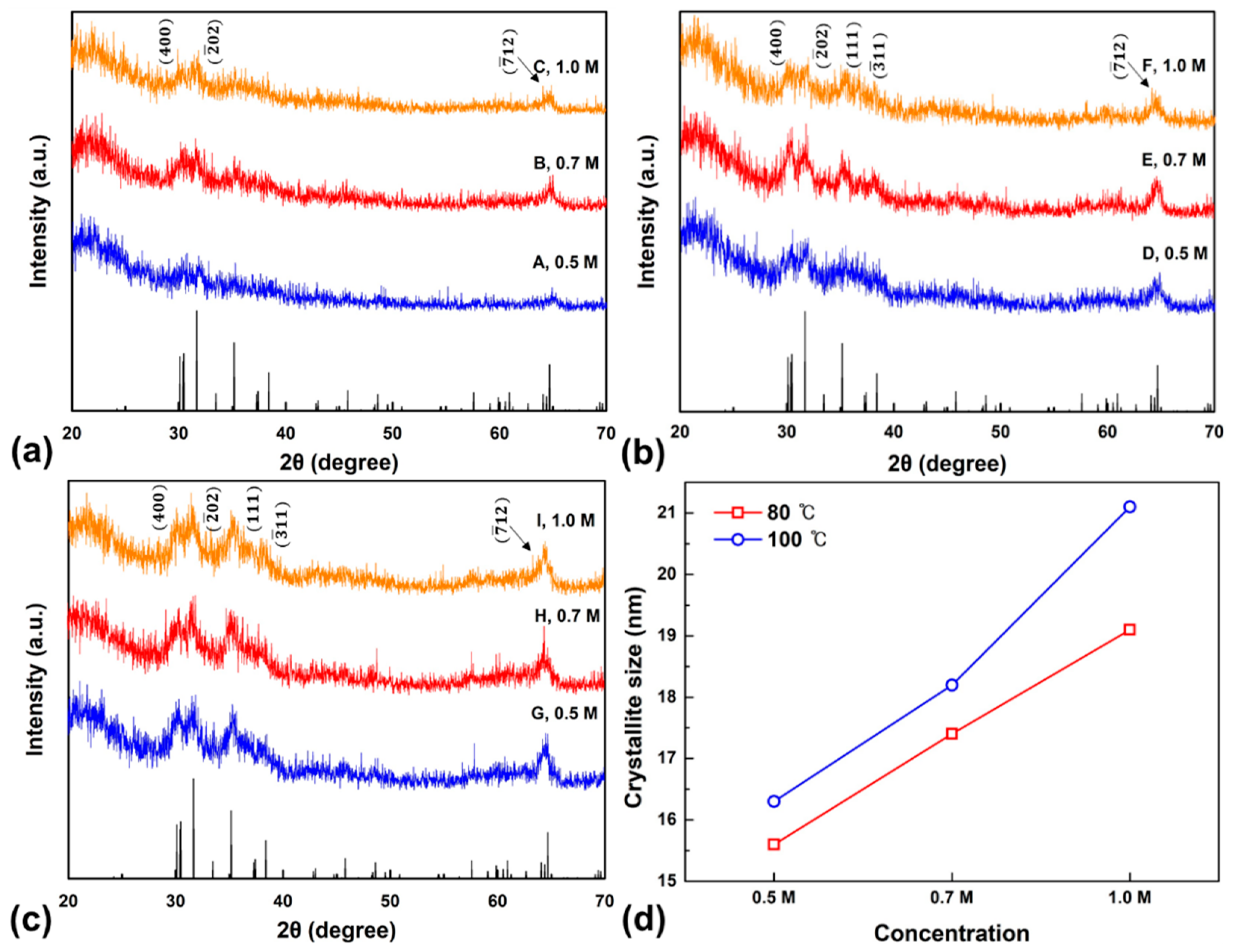
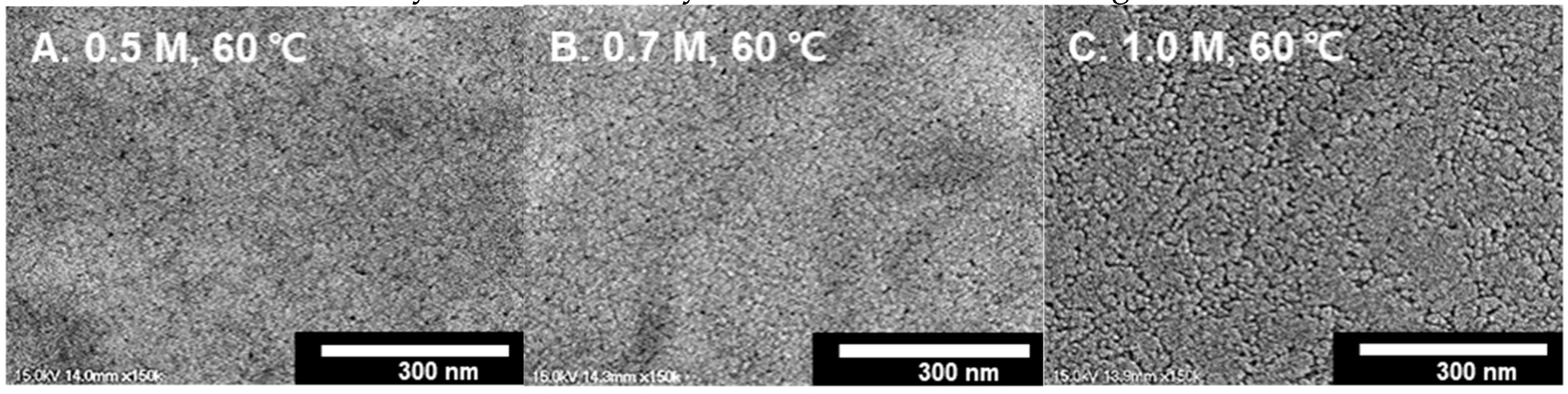
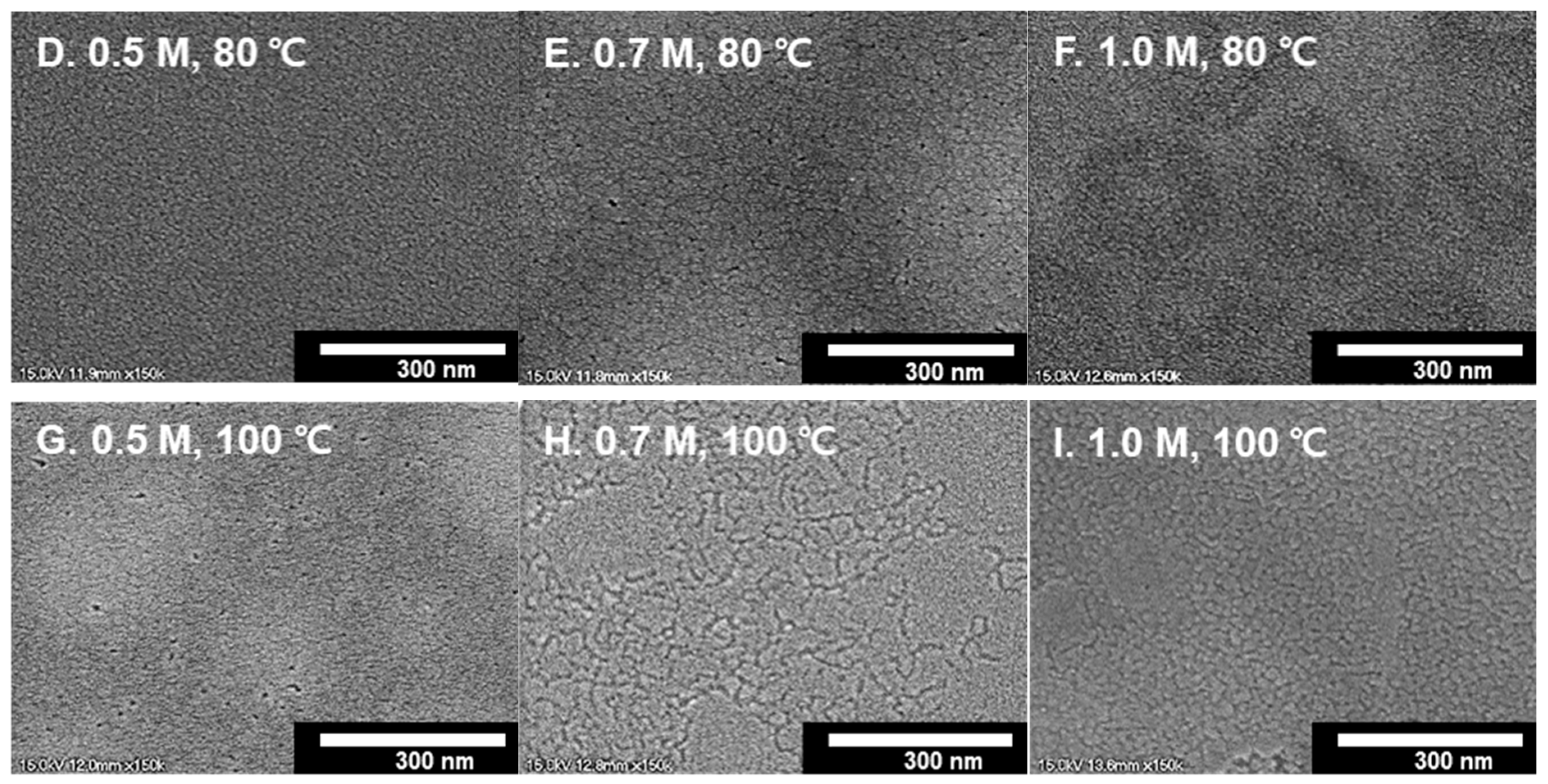
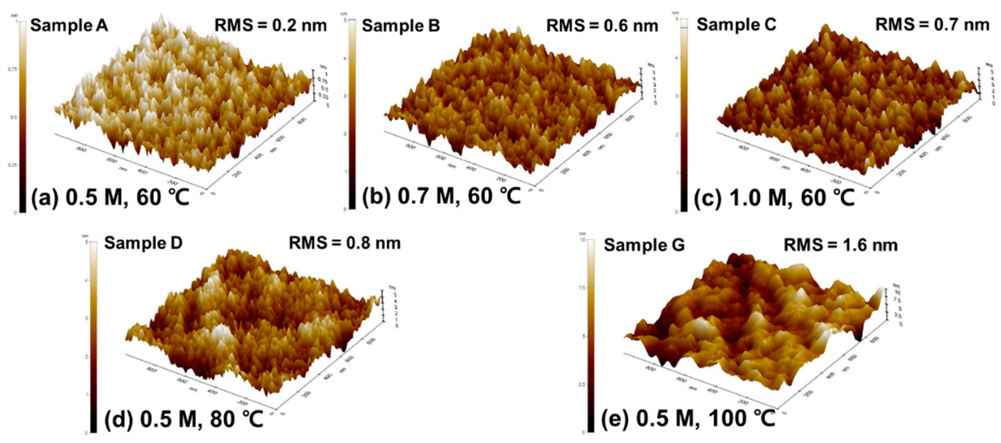
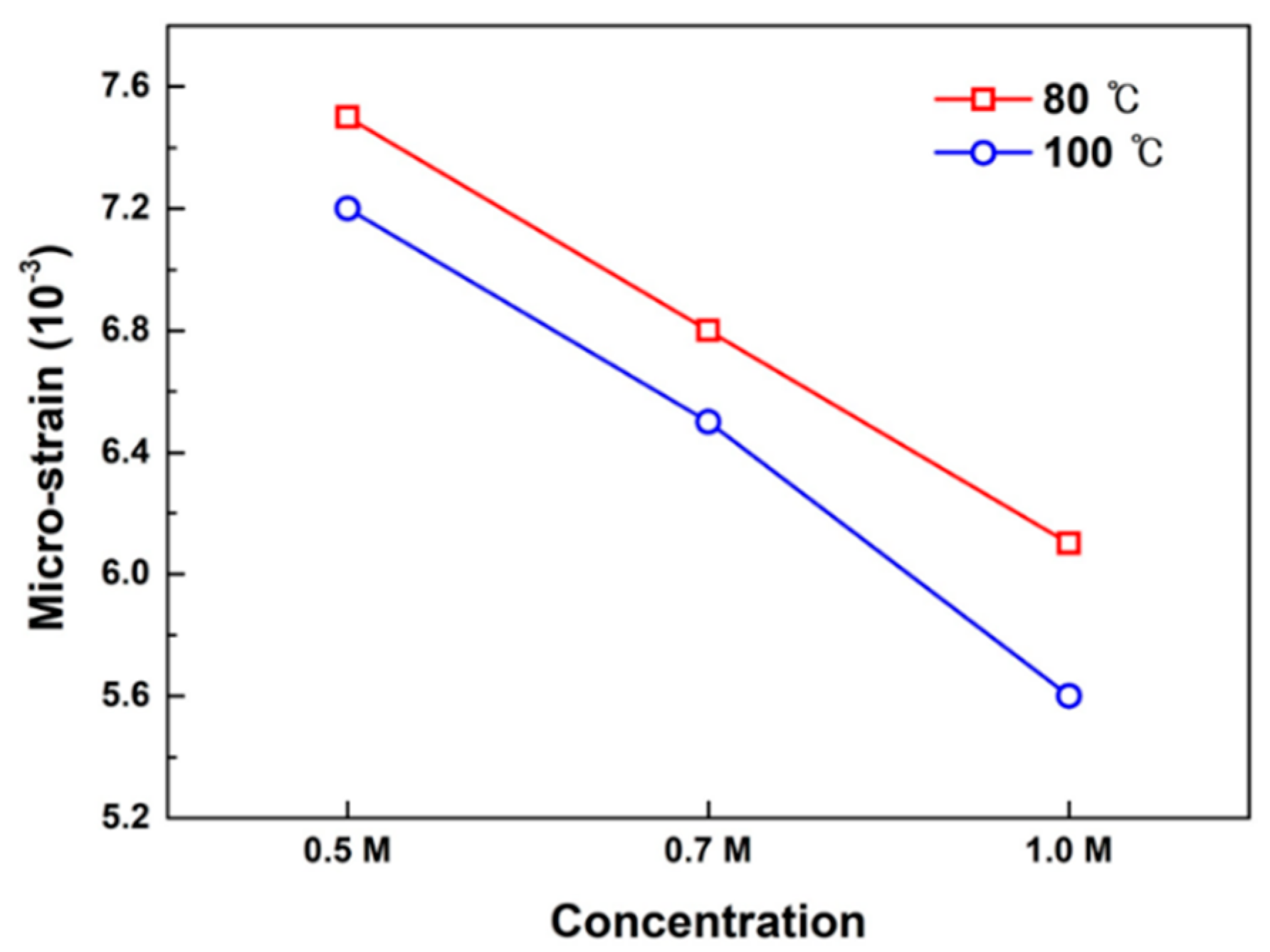
3.1. Structural Properties
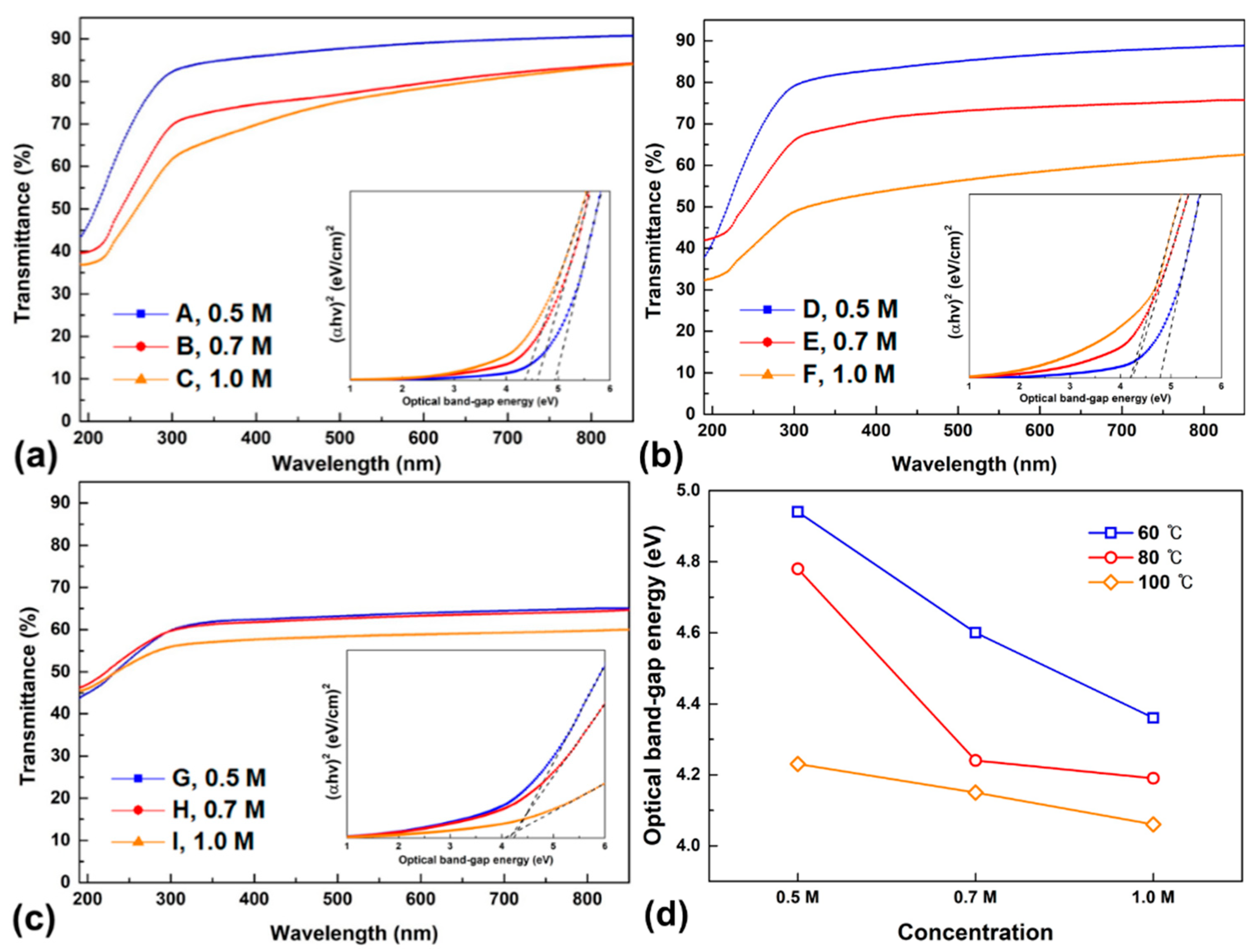
3.2. Optical Properties
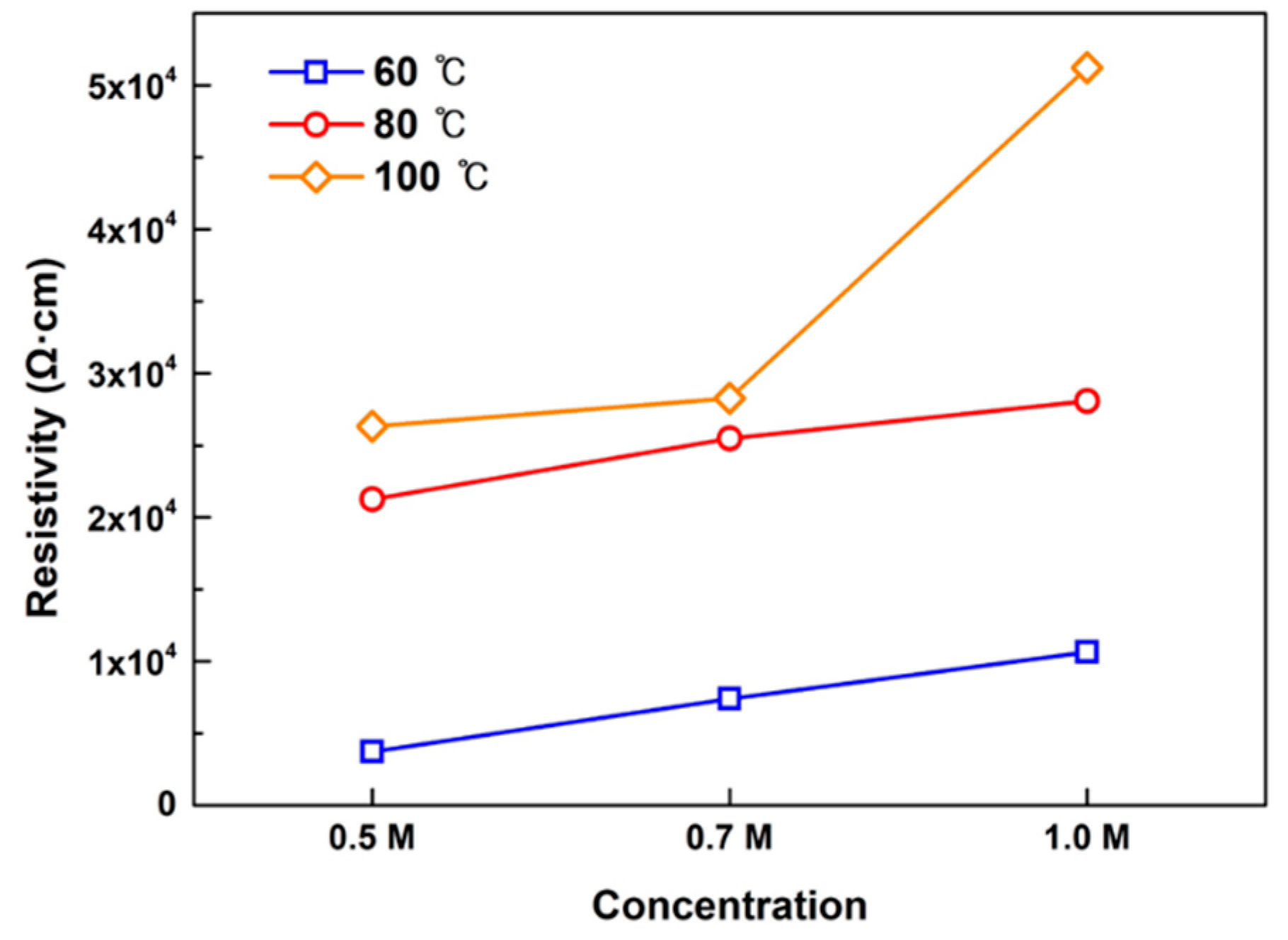
3.3. Electrical Properties
4. Conclusions
Author Contributions
Funding
Institutional Review Board Statement
Informed Consent Statement
Acknowledgments
Conflicts of Interest
References
- Oh, S.; Yang, G.; Kim, J. Electrical characteristics of vertical Ni/β-Ga2O3 schottky barrier diodes at high temperatures. ECS J. Solid State Sci. Technol. 2016, 6, Q3022. [Google Scholar] [CrossRef]
- Thomas, S.R.; Adamopoulos, G.; Lin, Y.-H.; Faber, H.; Sygellou, L.; Stratakis, E.; Pliatsikas, N.; Patsalas, P.A.; Anthopoulos, T.D. High electron mobility thin-film transistors based on Ga2O3 grown by atmospheric ultrasonic spray pyrolysis at low temperatures. Appl. Phys. Lett. 2014, 105, 092105. [Google Scholar] [CrossRef]
- Pratiyush, A.S.; Krishnamoorthy, S.; Muralidharan, R.; Rajan, S.; Nath, D.N. Advances in Ga2O3 solar-blind UV photodetectors. In Gallium Oxide; Elsevier: Amsterdam, The Netherland, 2019; pp. 369–399. [Google Scholar]
- Yu, M.; Lv, C.; Yu, J.; Shen, Y.; Yuan, L.; Hu, J.; Zhang, S.; Cheng, H.; Zhang, Y.; Jia, R. High-performance photodetector based on sol–gel epitaxially grown α/β Ga2O3 thin films. Mater. Today Commun. 2020, 25, 101532. [Google Scholar] [CrossRef]
- Jang, Y.-G.; Kim, W.-S.; Kim, D.-H.; Hong, S.-H. Fabrication of Ga2O3/SnO2 core–shell nanowires and their ethanol gas sensing properties. J. Mater. Res. 2011, 26, 2322–2327. [Google Scholar] [CrossRef]
- Wellmann, P.J. Power Electronic Semiconductor Materials for automotive and energy saving applications-SiC, GaN, Ga2O3, and diamond. Z. Anorg. Allg. Chem. 2017, 643, 1312–1322. [Google Scholar] [CrossRef] [PubMed] [Green Version]
- Yoshioka, S.; Hayashi, H.; Kuwabara, A.; Oba, F.; Matsunaga, K.; Tanaka, I. Structures and energetics of Ga2O3 polymorphs. J. Phys. Condens. Matter 2007, 19, 346211. [Google Scholar] [CrossRef]
- Ueda, N.; Hosono, H.; Waseda, R.; Kawazoe, H. Synthesis and control of conductivity of ultraviolet transmitting β-Ga2O3 single crystals. Appl. Phys. Lett. 1997, 70, 3561–3563. [Google Scholar] [CrossRef]
- Baliga, B.J. Power semiconductor device figure of merit for high-frequency applications. IEEE Electron Device Lett. 1989, 10, 455–457. [Google Scholar] [CrossRef]
- Johnson, E.O. Physical limitations on frequency and power parameters of transistors. In Semiconductor Devices: Pioneering Papers; World Scientific: Singapore, 1991; pp. 295–302. [Google Scholar]
- Xu, C.X.; Shen, L.Y.; Liu, H.; Pan, X.H.; Ye, Z.Z. High-Quality beta-Ga2O3 films with influence of growth temperature by pulsed laser deposition for solar-blind photodetectors. J. Electron. Mater. 2021, 50, 2043–2048. [Google Scholar] [CrossRef]
- Rafique, S.; Han, L.; Tadjer, M.J.; Freitas, J.A.; Mahadik, N.A.; Zhao, H.P. Homoepitaxial growth of beta-Ga2O3 thin films by low pressure chemical vapor deposition. Appl. Phys. Lett. 2016, 108, 182105. [Google Scholar] [CrossRef]
- Tadjer, M.J.; Alema, F.; Osinsky, A.; Mastro, M.A.; Nepal, N.; Woodward, J.M.; Myers-Ward, R.L.; Glaser, E.R.; Freitas, J.A.; Jacobs, A.G.; et al. Characterization of beta-Ga2O3 homoepitaxial films and MOSFETs grown by MOCVD at high growth rates. J. Phys. D Appl. Phys. 2021, 54, 034005. [Google Scholar] [CrossRef]
- Schurig, P.; Michel, F.; Beyer, A.; Volz, K.; Becker, M.; Polity, A.; Klar, P.J. Progress in sputter growth of beta-Ga2O3 by applying pulsed-mode operation. Phys. Status Solidi A 2020, 217, 1901009. [Google Scholar] [CrossRef]
- Hong, J.; Wagata, H.; Katsumata, K.; Okada, K.; Matsushita, N. Effects of thermal treatment on crystallographic and electrical properties of transparent conductive ZnO films deposited by spin-spray method. Jpn. J. Appl. Phys. 2013, 52, 110108. [Google Scholar] [CrossRef] [Green Version]
- Hong, J.S.; Wagata, H.; Ohashi, N.; Katsumata, K.; Okada, K.; Matsushita, N. Transparent ZnO films deposited by aqueous solution process under various pH conditions. J. Electron Mater. 2015, 44, 2657–2662. [Google Scholar] [CrossRef]
- Chen, D.Z.; Xu, Y.; An, Z.Y.; Li, Z.; Zhang, C.F. Thin-film transistors based on wide bandgap Ga2O3 films grown by aqueous-solution spin-coating method. Micro. Nano Lett. 2019, 14, 1052–1055. [Google Scholar] [CrossRef]
- Pandeeswari, R.; Jeyaprakash, B. High sensing response of β-Ga2O3 thin film towards ammonia vapours: Influencing factors at room temperature. Sens. Actuators B Chem. 2014, 195, 206–214. [Google Scholar] [CrossRef]
- Park, S.-S.; Mackenzie, J. Sol-gel-derived tin oxide thin films. Thin Solid Films 1995, 258, 268–273. [Google Scholar] [CrossRef]
- Hong, J.; Lin, H.E.; Katsumata, K.; Matsushita, N. The study of correlation between electrical conductivity of solution-processed ZnO film and UV irradiation. Mat. Sci. Semicon. Proc. 2020, 120, 105266. [Google Scholar] [CrossRef]
- Rico, V.; López, C.; Borrás, A.; Espinos, J.; González-Elipe, A. Effect of visible light on the water contact angles on illuminated oxide semiconductors other than TiO2. Sol. Energy Mater. Sol. Cells 2006, 90, 2944–2949. [Google Scholar] [CrossRef]
- Khranovskyy, V.; Ekblad, T.; Yakimova, R.; Hultman, L. Surface morphology effects on the light-controlled wettability of ZnO nanostructures. Appl. Surf. Sci. 2012, 258, 8146–8152. [Google Scholar]
- Ohya, Y.; Okano, J.; Kasuya, Y.; Ban, T. Fabrication of Ga2O3 thin films by aqueous solution deposition. J. Ceram. Soc. Jpn. 2009, 117, 973–977. [Google Scholar] [CrossRef] [Green Version]
- Patil, P.; Park, J.; Lee, S.Y.; Park, J.-K.; Cho, S.-H. White light generation from single gallium oxide nanoparticles co-doped with rare-earth metals. Appl. Sci. Converg. Technol. 2014, 23, 296–300. [Google Scholar] [CrossRef]
- Cullity, B.D. Elements of X-ray Diffraction; Addison-Wesley Publishing: Boston, MA, USA, 1956. [Google Scholar]
- Dhaouadi, M.; Jlassi, M.; Sta, I.; Miled, I.B.; Mousdis, G.; Kompitsas, M.; Dimassi, W. Physical properties of copper oxide thin films prepared by sol–gel spin–coating method. Am. J. Phys. Appl. 2018, 6, 43–50. [Google Scholar] [CrossRef] [Green Version]
- Necib, K.; Touam, T.; Chelouche, A.; Ouarez, L.; Djouadi, D.; Boudine, B. Investigation of the effects of thickness on physical properties of AZO sol-gel films for photonic device applications. J. Alloys Compd. 2018, 735, 2236–2246. [Google Scholar] [CrossRef]
- Korotcenkov, G.; Brinzari, V.; Cerneavschi, A.; Ivanov, M.; Golovanov, V.; Cornet, A.; Morante, J.; Cabot, A.; Arbiol, J. The influence of film structure on In2O3 gas response. Thin Solid Films 2004, 460, 315–323. [Google Scholar] [CrossRef]
- Kong, K.; Deka, B.K.; Kim, M.; Oh, A.; Kim, H.; Park, Y.-B.; Park, H.W. Interlaminar resistive heating behavior of woven carbon fiber composite laminates modified with ZnO nanorods. Compos. Sci. Technol. 2014, 100, 83–91. [Google Scholar] [CrossRef]
- Zhang, H.; Wang, Y.; Wang, H.; Ma, M.; Dong, S.; Xu, Q. Influence of drying temperature on morphology of MAPbI3 thin films and the performance of solar cells. J. Alloys Compd. 2019, 773, 511–518. [Google Scholar] [CrossRef] [Green Version]
- Dekeijser, M.; Dormans, G.J.M.; Vanveldhoven, P.J.; Deleeuw, D.M. Effects of crystallite size in PbTiO3 thin-films. Appl. Phys. Lett. 1991, 59, 3556–3558. [Google Scholar] [CrossRef]
- Bouderbala, M.; Hamzaoui, S.; Amrani, B.; Reshak, A.H.; Adnane, M.; Sahraoui, T.; Zerdali, M. Thickness dependence of structural, electrical and optical behaviour of undoped ZnO thin films. Phys. B 2008, 403, 3326–3330. [Google Scholar] [CrossRef]
- Guo, P.; Xiong, J.; Zhao, X.; Sheng, T.; Yue, C.; Tao, B.; Liu, X. Growth Characteristics and Device Properties of MOD Derived β-Ga2O3 Films. J. Mater. Sci.: Mater. Electron. 2014, 25, 3629–3632. [Google Scholar] [CrossRef]
- Chen, H.; Baitenov, A.; Li, Y.Y.; Vasileva, E.; Popov, S.; Sychugov, I.; Yan, M.; Berglund, L. Thickness dependence of optical transmittance of transparent wood: Chemical modification effects. ACS Appl. Mater. Interf. 2019, 11, 35451–35457. [Google Scholar] [CrossRef] [PubMed]
- Liu, Y.; Tung, S.; Hsieh, J. Influence of annealing on optical properties and surface structure of ZnO thin films. J. Cryst. Growth 2006, 287, 105–111. [Google Scholar] [CrossRef]
- Mastro, M.A.; Kuramata, A.; Calkins, J.; Kim, J.; Ren, F.; Peartong, S.J. Opportunities and future directions for Ga2O3. Ecs J. Solid State Sci. Technol. 2017, 6, P356–P359. [Google Scholar] [CrossRef]
- Pearton, S.J.; Yang, J.C.; Cary, P.H.; Ren, F.; Kim, J.; Tadjer, M.J.; Mastro, M.A. A review of Ga2O3 materials, processing, and devices. Appl. Phys. Rev. 2018, 5, 011301. [Google Scholar] [CrossRef] [Green Version]
- Higashiwaki, M.; Jessen, G.H. Guest Editorial: The dawn of gallium oxide microelectronics. Appl. Phys. Lett. 2018, 112, 6. [Google Scholar] [CrossRef] [Green Version]
- Kayani, Z.N.; Iqbal, M.; Riaz, S.; Zia, R.; Naseem, S. Fabrication and properties of zinc oxide thin film prepared by sol-gel dip coating method. Mater. Sci.-Pol. 2015, 33, 515–520. [Google Scholar] [CrossRef]
- Shin, J.; Kim, K.; Hong, J. Zn-Al Layered double hydroxide thin film fabricated by the sputtering method and aqueous solution treatment. Coatings 2020, 10, 669. [Google Scholar] [CrossRef]
- Martinez, M.; Herrero, J.; Gutierrez, M. Properties of RF sputtered zinc oxide based thin films made from different targets. Sol. Energy Mater. Sol. Cells 1994, 31, 489–498. [Google Scholar] [CrossRef]
- Lokhande, B.; Uplane, M. Structural, optical and electrical studies on spray deposited highly oriented ZnO films. Appl. Surf. Sci. 2000, 167, 243–246. [Google Scholar] [CrossRef]
- Qu, Y.; Gessert, T.; Coutts, T.; Noufi, R. Study of ion-beam-sputtered ZnO films as a function of deposition temperature. J. Vac. Sci. Technol. A Vac. Surf. Films 1994, 12, 1507–1512. [Google Scholar] [CrossRef]
- Ashour, A.; Kaid, M.A.; El-Sayed, N.Z.; Ibrahim, A.A. Physical properties of ZnO thin films deposited by spray pyrolysis technique. Appl. Surf. Sci. 2006, 252, 7844–7848. [Google Scholar] [CrossRef]
- Mi, W.; Du, X.; Luan, C.; Xiao, H.; Ma, J. Electrical and optical characterizations of β-Ga2O3: Sn films deposited on MgO (110) substrate by MOCVD. RSC Adv. 2014, 4, 30579–30583. [Google Scholar] [CrossRef]


| Sample | A | B | C | D | E | F | G | H | I |
|---|---|---|---|---|---|---|---|---|---|
| Drying temperature (°C) | 60 | 80 | 100 | ||||||
| Precursor concentration (M) | 0.5 | 0.7 | 1.0 | 0.5 | 0.7 | 1.0 | 0.5 | 0.7 | 1.0 |
| Sample | A | B | C | D | E | F | G | H | I |
|---|---|---|---|---|---|---|---|---|---|
| Thickness (nm) | 52 | 65 | 70 | 120 | 130 | 176 | 238 | 254 | 412 |
Publisher’s Note: MDPI stays neutral with regard to jurisdictional claims in published maps and institutional affiliations. |
© 2021 by the authors. Licensee MDPI, Basel, Switzerland. This article is an open access article distributed under the terms and conditions of the Creative Commons Attribution (CC BY) license (https://creativecommons.org/licenses/by/4.0/).
Share and Cite
Park, T.; Kim, K.; Hong, J. Effects of Drying Temperature and Molar Concentration on Structural, Optical, and Electrical Properties of β-Ga2O3 Thin Films Fabricated by Sol–Gel Method. Coatings 2021, 11, 1391. https://doi.org/10.3390/coatings11111391
Park T, Kim K, Hong J. Effects of Drying Temperature and Molar Concentration on Structural, Optical, and Electrical Properties of β-Ga2O3 Thin Films Fabricated by Sol–Gel Method. Coatings. 2021; 11(11):1391. https://doi.org/10.3390/coatings11111391
Chicago/Turabian StylePark, Taejun, Kyunghwan Kim, and Jeongsoo Hong. 2021. "Effects of Drying Temperature and Molar Concentration on Structural, Optical, and Electrical Properties of β-Ga2O3 Thin Films Fabricated by Sol–Gel Method" Coatings 11, no. 11: 1391. https://doi.org/10.3390/coatings11111391
APA StylePark, T., Kim, K., & Hong, J. (2021). Effects of Drying Temperature and Molar Concentration on Structural, Optical, and Electrical Properties of β-Ga2O3 Thin Films Fabricated by Sol–Gel Method. Coatings, 11(11), 1391. https://doi.org/10.3390/coatings11111391