
Morphological and Structural Evolution of Chemically Deposited Epitaxially LaNiO3 Thin Films

 ,
, 
Abstract
:1. Introduction
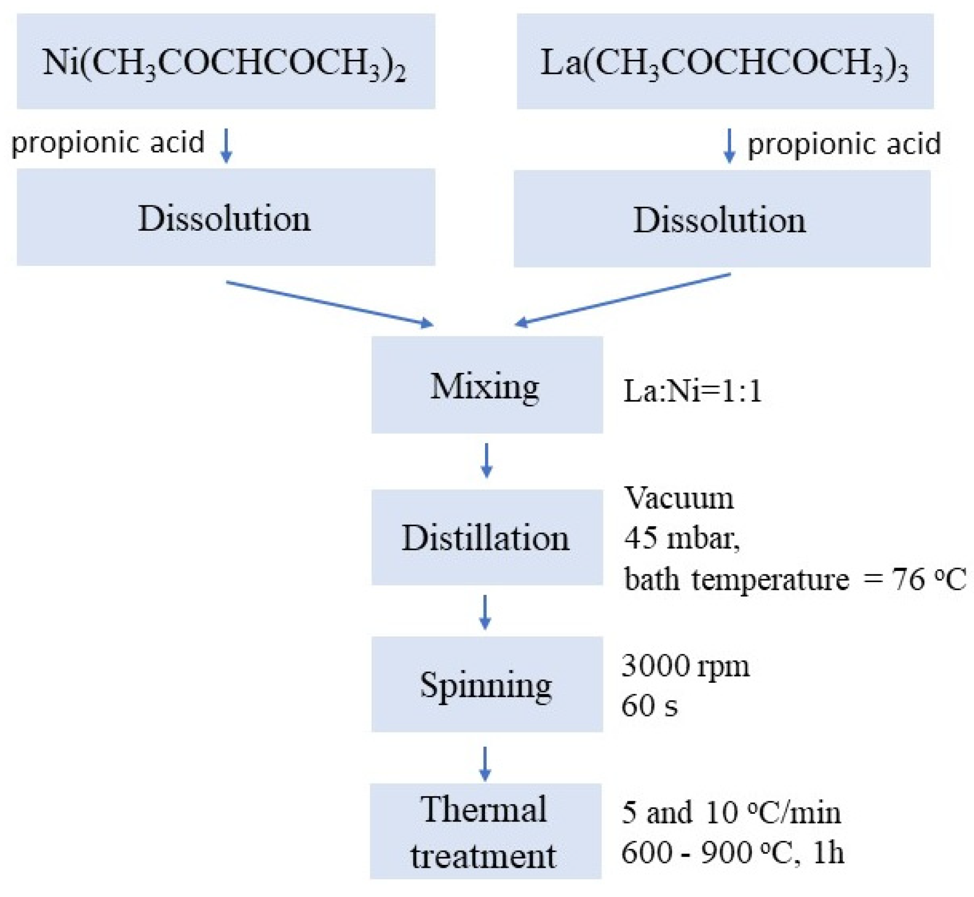
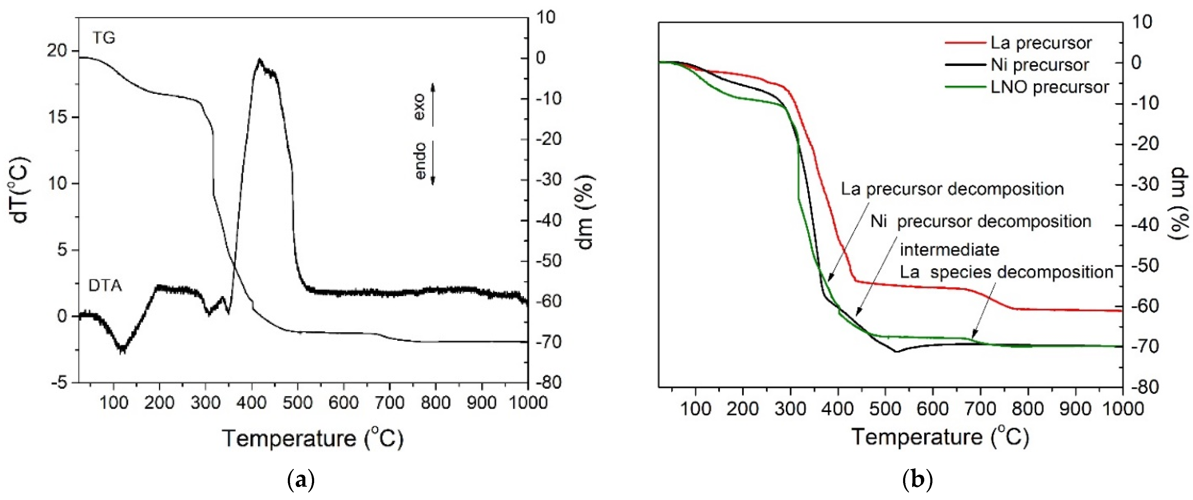
2. Experimental
3. Results and Discussion
3.1. Thin Films Deposition and Characterization
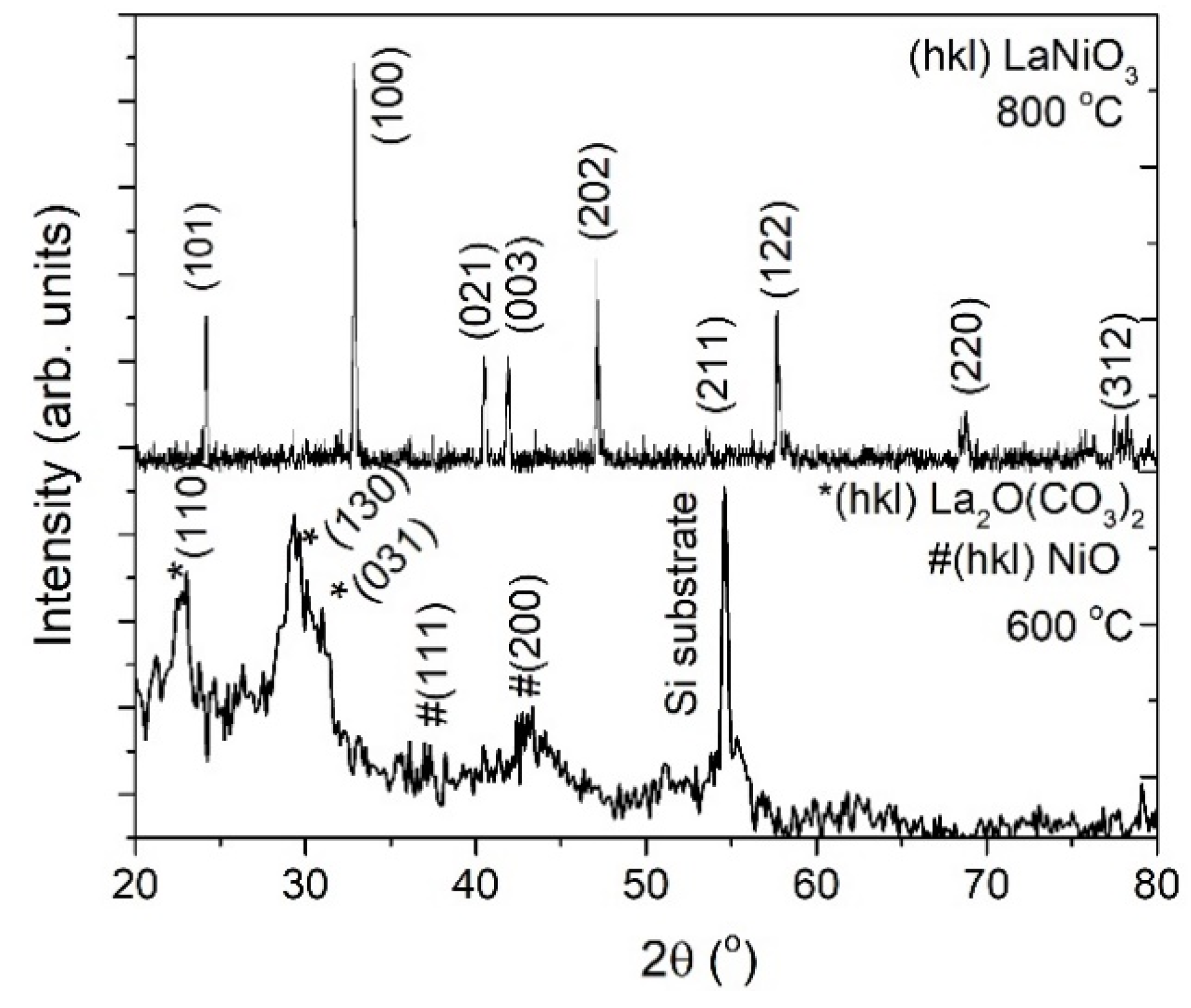
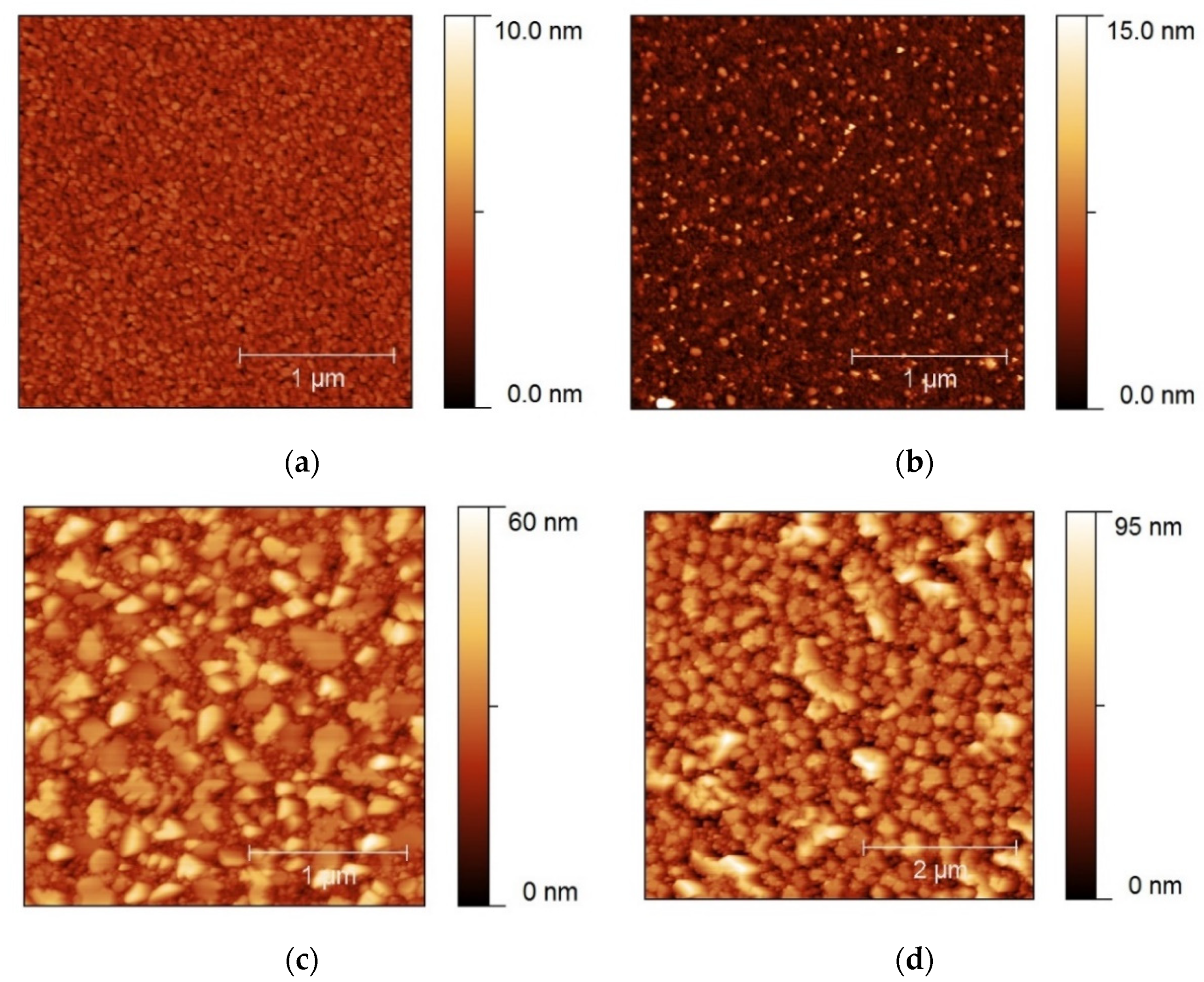
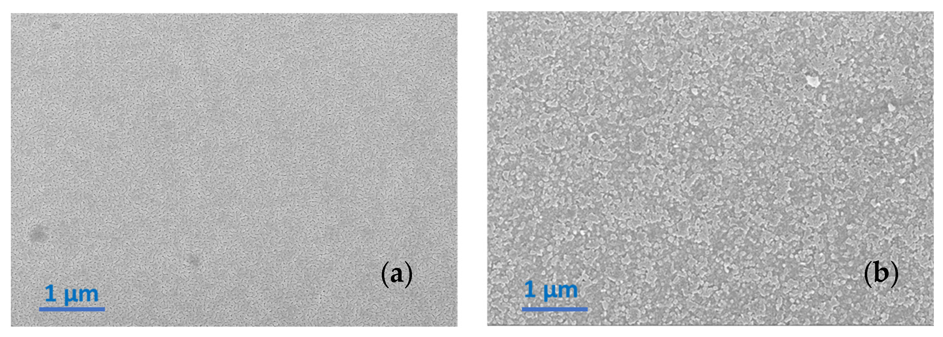
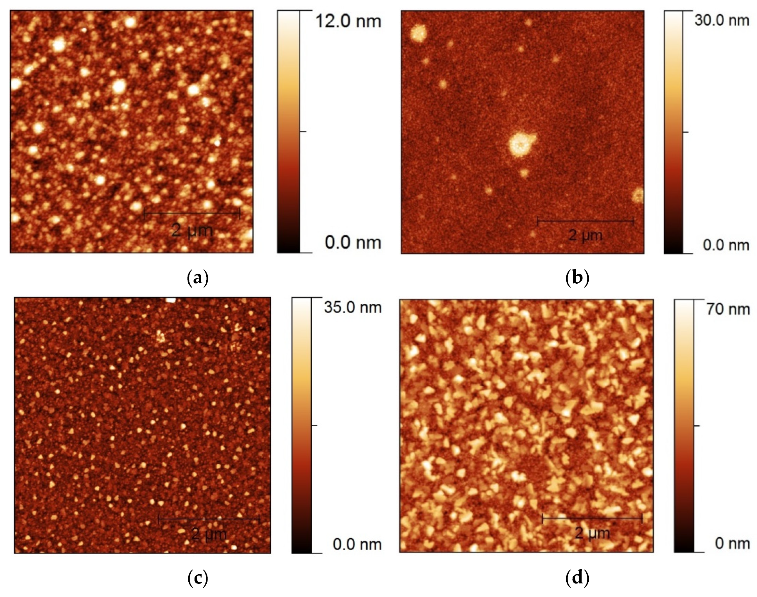
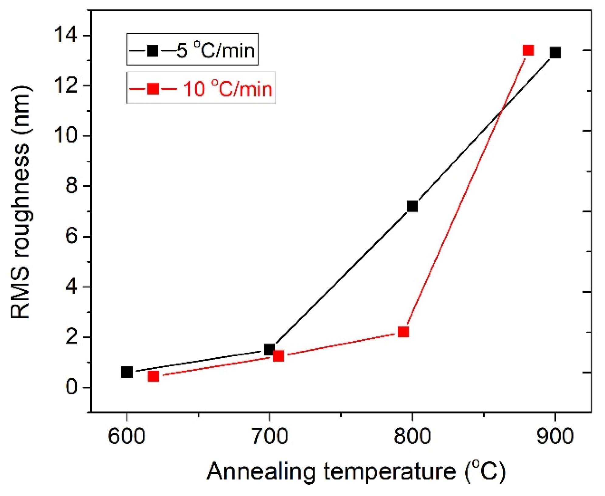
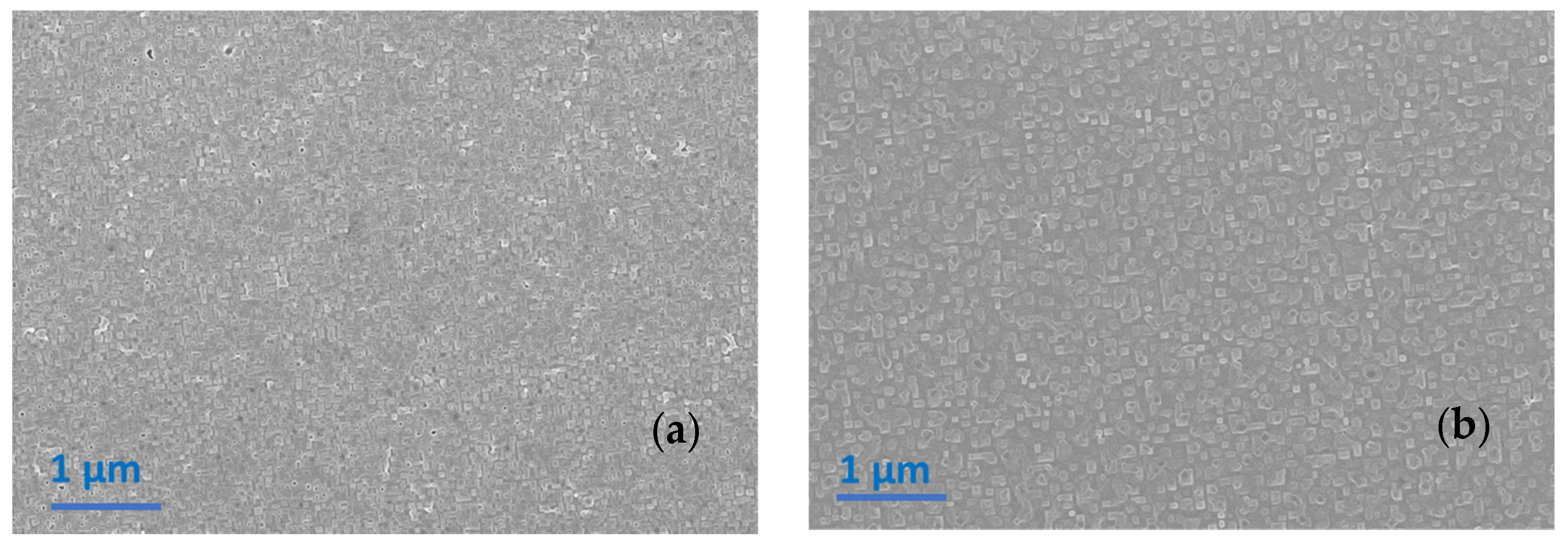
3.1.1. Heating Ramp: 5 °C/min
3.1.2. Heating Ramp: 10 °C/min
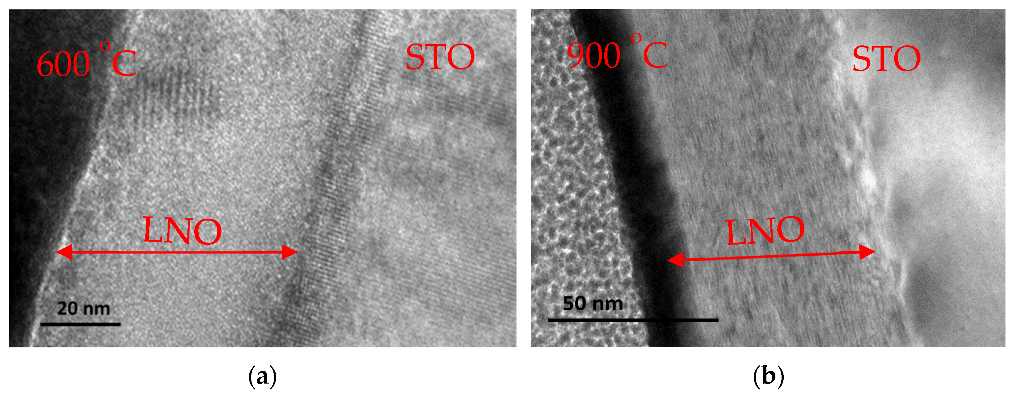
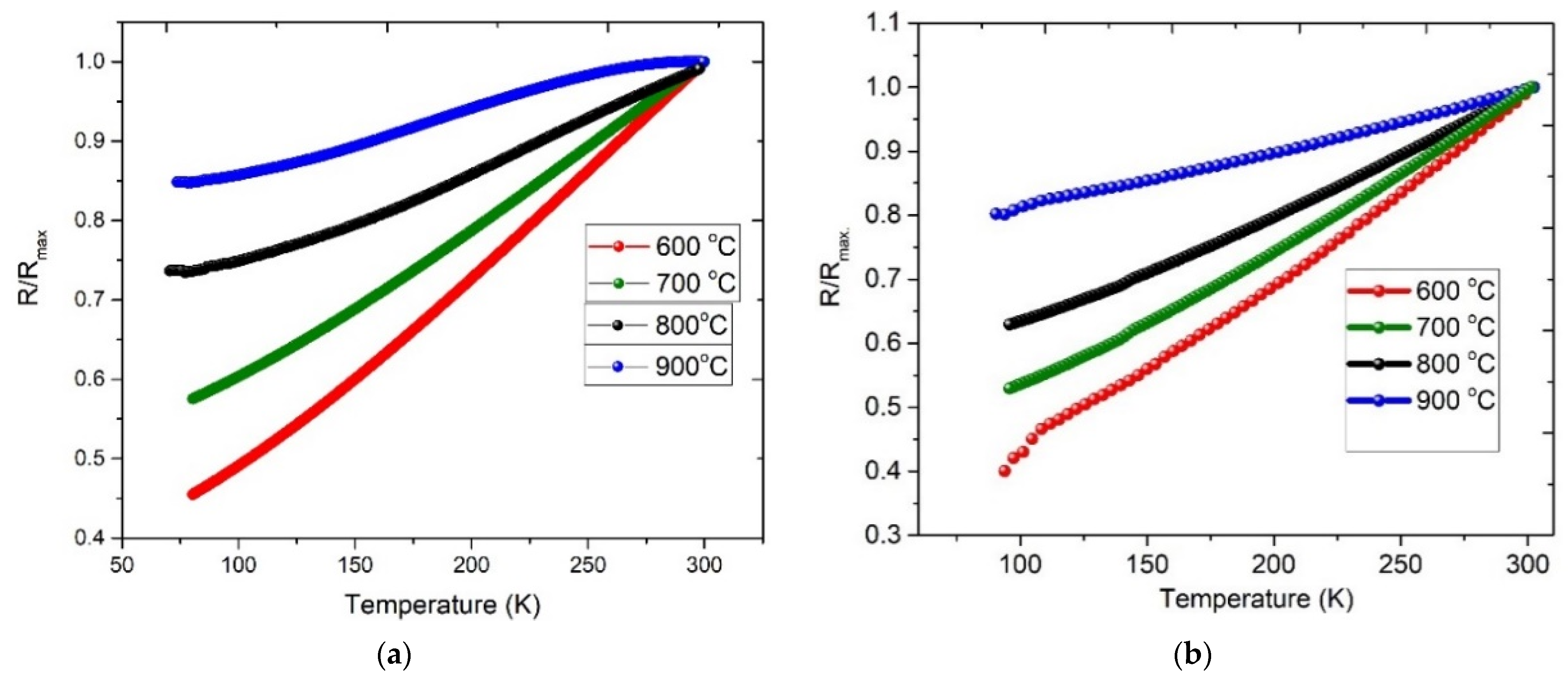
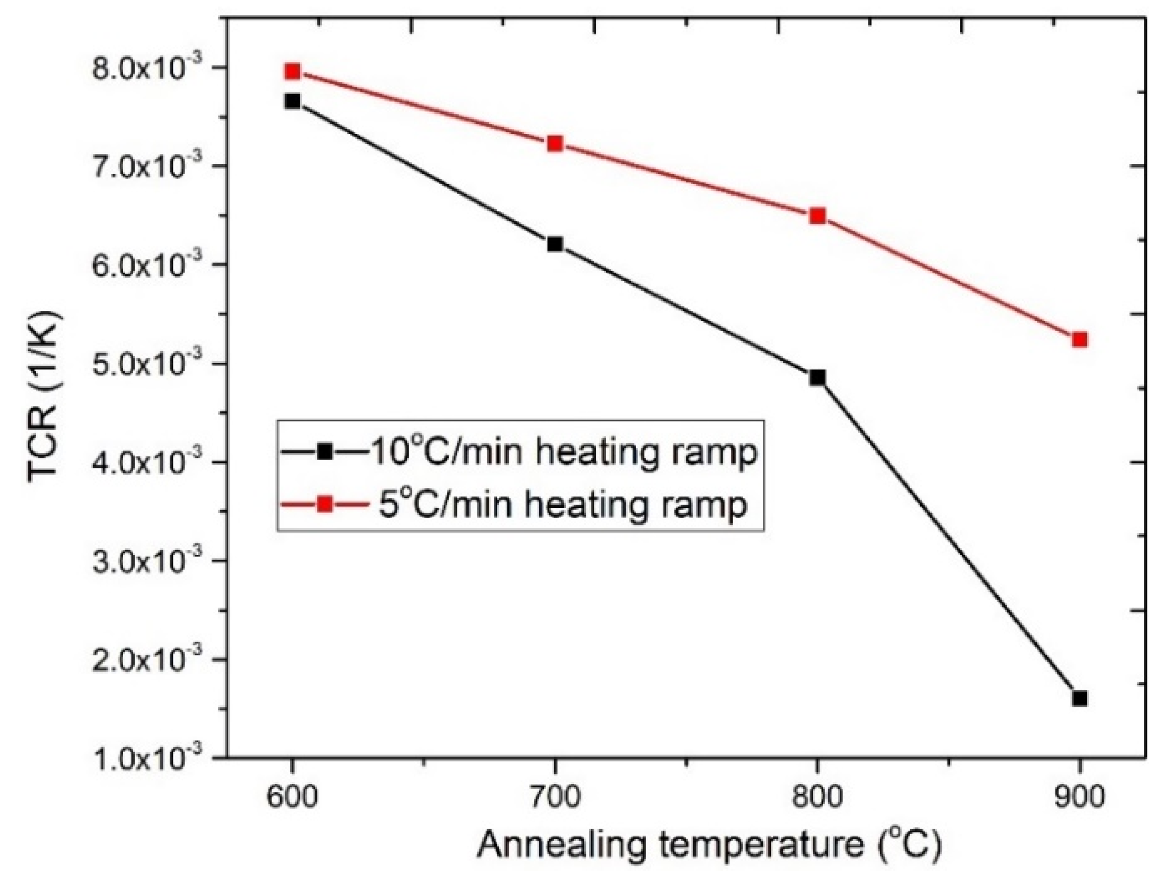
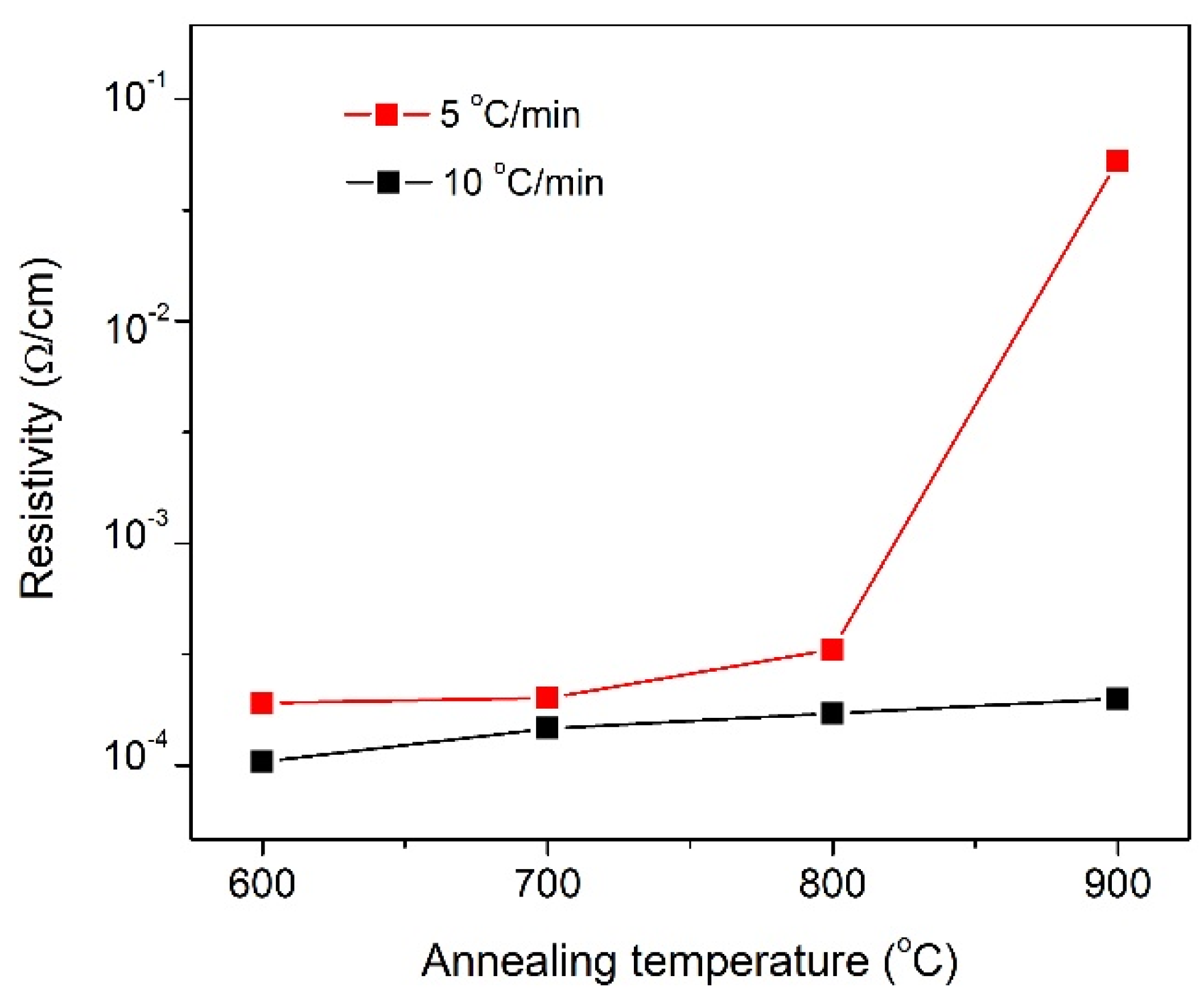
3.1.3. Electrical Characterization
4. Conclusions
Author Contributions
Funding
Institutional Review Board Statement
Informed Consent Statement
Data Availability Statement
Conflicts of Interest
References
- Wold, A.; Post, B.; Banks, E. Rare Earth Nickel Oxides. J. Am. Chem. Soc. 1957, 79, 4911–4913. [Google Scholar] [CrossRef]
- KRajeev, P.; Shivashankar, G.V.; Raychaudhuri, A.K. Low-temperature electronic properties of a normal conducting perovskite oxide (LaNiO3). Solid State Commun. 1991, 79, 591–595. [Google Scholar] [CrossRef]
- Catalan, G. Progress in perovskite nickelate research. Phase Transit. 2008, 81, 729–749. [Google Scholar] [CrossRef]
- Zhu, T.J.; Lu, L. X-ray Diffraction and Photoelectron Spectroscopic Studies of (001)-Oriented Pb(Zr0.52Ti0.48)O3 Thin Films Prepared by Laser Ablation. J. Appl. Phys. 2004, 95, 241–247. [Google Scholar] [CrossRef]
- Cichetto, L., Jr.; Sergeenkov, S.; Diaz, J.C.C.A.; Longo, E.; Araújo-Moreira, F.M. Influence of substrate on structural and transport properties of LaNiO3 thin films prepared by pulsed laser deposition. AIP Adv. 2017, 7, 025005. [Google Scholar] [CrossRef] [Green Version]
- Guo, H.; Li, Z.W.; Zhao, L.; Hu, Z.; Chang, C.F.; Kue, C.-Y.; Schmidt, W.; Piovano, A.; Pi, T.W.; Sobolev, O.; et al. Antiferromagnetic correlations in the metallic strongly correlated transition metal oxide LaNiO3. Nat. Commun. 2018, 9, 9–43. [Google Scholar] [CrossRef] [PubMed]
- Wu, C.M.; Hong, T.J.; Wu, T.B. Effects of (100)-textured LaNiO3 electrode on the deposition and characteristics of PbTiO3 thin films prepared by RF magnetron sputtering. J. Mater. Res. 1997, 12, 2158–2164. [Google Scholar] [CrossRef]
- Hwang, K.; Lim, Y.; Kim, B. Epitaxially grown LaNiO3 thin films on SrTiO3(100) substrates by the chemical solution method. Mater. Res. Bull. 1999, 34, 2069–2074. [Google Scholar] [CrossRef]
- Drennan, J.; Tavares, C.P.; Steele, B.C.H. An electron microscope investigation of phases in the system La–Ni–O. Mater. Res. Bull. 1982, 7, 621. [Google Scholar] [CrossRef]
- Satyalakshmi, K.M.; Mallya, R.M.; Ramanathan, K.V.; Wu, X.D.; Brainard, B.; Gautier, D.C.; Vasanthacharya, N.Y.; Hegde, M.S. Epitaxial metallic LaNiO3 thin films grown by pulsed laser deposition. Appl. Phys. Lett. 1993, 62, 1233. [Google Scholar] [CrossRef]
- Chen, P.; Xu, S.Y.; Zhou, W.Z.; Ong, C.K.; Cui, D.F. In situ reflection high-energy electron diffraction observation of epitaxial LaNiO3 thin films. J. Appl. Phys. 1999, 85, 3000−3002. [Google Scholar] [CrossRef]
- Dobin, A.Y.; Nikolaev, K.R.; Krivorotov, N.; Wentzcovitch, R.M.; Dahlberg, E.D.; Goldman, A.M. Electronic and crystal structure of fully strained LaNiO3 films. Phys. Rev. B 2003, 68, 113408. [Google Scholar] [CrossRef]
- Aiyer, H.N.; Raju, A.R.; Subbanna, G.N.; Rao, C.N.R. Novel materials, materials design and synthetic strategies: Recent advances and new directions. Chem. Mater. 1997, 9, 755. [Google Scholar] [CrossRef]
- Schwartz, R.W.; Schneller, T.; Waser, R. Chemical solution deposition of electronic oxide films. Comptes Rendus Chim. 2004, 7, 433–461. [Google Scholar] [CrossRef]
- Meng, X.J.; Sun, J.L.; Yu, J.; Ye, H.J.; Guo, S.L.; Chu, J.H. Preparation of highly (100)-oriented metallic LaNiO3 films on Si substrates by a modified metalorganic decomposition technique. Appl. Surf. Sci. 2001, 171, 68–70. [Google Scholar] [CrossRef]
- Ueno, K.; Yamaguchi, T.; Sakamoto, W.; Yogo, T.; Kikuta, K.; Hirano, S. Orientation control of chemical solution deposited LaNiO3 thin films. Thin Solid Film. 2005, 491, 78–81. [Google Scholar] [CrossRef]
- Li, A.-D.; Ge, C.-Z.; Di Wu, P.L.; Zuo, Y.-Q.; Yang, S.-Z.; Ming, N.-B. Conductive metallic LaNiO3 films from metallo-organic precursors. Thin Solid Film. 1997, 298, 165–169. [Google Scholar] [CrossRef]
- Amoresi, R.A.C.; Felix, A.A.; Lustosa, G.M.M.M.; Gasparotto, G.; Simões, A.Z.; Zaghete, M.A. Role of morphological characteristics on the conductive behavior of LaNiO3 thin films. Ceram. Int. 2016, 42, 16242–16247. [Google Scholar] [CrossRef] [Green Version]
- Kuprenaite, S.; Astié, V.; Margueron, S.; Millon, C.; Decams, J.-M.; Saltyte, Z.; Boulet, P.; Plausinaitiene, V.; Abrutis, A.; Bartasyte, A. Relationship processing–composition–structure–resistivity of LaNiO3 thin films grown by chemical vapor deposition methods. Coating 2019, 9, 35. [Google Scholar] [CrossRef] [Green Version]
- Park, J.; Lim, Y.; Kong, S.; Lee, H.; Kim, Y.-B. Rapid fabrication of chemical solution-deposited lanthanum nickelate thin films via intense pulsed-light process. Coating 2019, 9, 372. [Google Scholar] [CrossRef] [Green Version]
- Tsubouchi, K.; Ohkubo, I.; Kumigashira, H.; Matsumoto, Y.; Ohnishi, T.; Lippmaa, M.; Koinuma, H.; Oshima, M. Epitaxial growth and surface metallic nature of LaNiO3 thin films. Appl. Phys. Lett. 2009, 92, 262109. [Google Scholar] [CrossRef]
- Qiao, L.; Bi, X. Direct observation of Ni3+ and Ni2+ in correlated LaNiO3−δ films. Europhys. Lett. 2011, 93, 57002. [Google Scholar] [CrossRef]
- Abbate, M.; Zampieri, G.; Prado, F.; Caneiro, A.; Gonzalez-Calbet, J.M.; Vallet-Regi, M. Electronic structure and metal-insulator transition in LaNiO3-delta. Phys. Rev. B 2002, 65, 155101. [Google Scholar] [CrossRef]
- Horcas, I.; Fernandez, R.; Gomez-Rodrìguez, J.M.; Colchero, J.; Gomez-Herrero, J.; Baro, A.M. WSXM: A software for scanning probe microscopy and a tool for nanotechnology. Rev. Sci. Instrum. 2007, 78, 013705. [Google Scholar] [CrossRef] [PubMed]
- Ciontea, L.; Nasui, M.; Petrisor, T., Jr.; Mos, R.B.; Gabor, M.S.; Varga, R.A.; Petrisor, T. Synthesis, crystal structure and thermal decomposition of La2(CH3CH2COO)6·(H2O)3]·3.5H2O precursor for high-k La2O3 thin films deposition. Mater. Res. Bull. 2010, 45, 1203–1208. [Google Scholar] [CrossRef]
- Sonher, R.B.; Nasui, M.; Gabor, M.S.; Petrisor, T., Jr.; Ciontea, L.; Petrisor, T. Effect of glycerol on the thermal decomposition behavior of nickel propionate-based precursor. J. Anal. Appl. Pyrol. 2021, 159, 105289. [Google Scholar] [CrossRef]
- Roura, P.; Farjas, J.; Eloussifi, H.; Carreras, L.; Ricart, S.; Puig, T.; Obradors, X. Thermal analysis of metal organic precursors for functional oxidepreparation: Thin films versus powders. Thermochim. Acta 2015, 601, 1–8. [Google Scholar] [CrossRef] [Green Version]
- Odier, P.; Nigara, Y.; Coutures, J. Phase relations in the La–Ni–O system: Influence of temperature and stoichiometry on the structure of La2NiO4. J. Solid State Chem. 1985, 56, 32–40. [Google Scholar] [CrossRef]
- Wu, G.; Ruan, K.; Liang, T.; Chen, X.; Bao, D. Preparation and conductive properties of neodymium-doped lanthanum nickelate thin films by chemical solution deposition method. Thin Solid Film. 2009, 517, 1563–1566. [Google Scholar] [CrossRef]
- Duan, Z.; Cui, Y.; Yang, Z.; Li, K.; Wan, Y.; Lu, Z.; Xie, Y.; Zhang, J. Growth of highlyc-axis oriented LaNiO3 films with improved surfacemorphology on Si substrate using chemical solution deposition and rapid heat treatment process. Ceram. Int. 2018, 44, 695–712. [Google Scholar] [CrossRef]
- Pocuca, M.; Brankovic, G.; Brankovic, Z.; Vasiljevic-Radovic, D.; Poleti, D. Optimization of processing parameters for preparation of LaNiO3 thin films from the citrate precursor. J. Eur. Ceram. Soc. 2007, 27, 1083–1086. [Google Scholar] [CrossRef]
- Hwang, K.-S.; Kang, B.-A.; Jeon, Y.-S.; An, J.-H.; Kim, B.-H.; Nishio, K.; Tsuchiya, T. AFM study of LaNiO3 thin films on various single crystal substrates prepared by using a metal naphthenate precursor. Surf. Coat. Technol. 2005, 190, 331–335. [Google Scholar] [CrossRef]
- Pontes, D.S.L.; Pontes, F.M.; Pereira-da-Silva, A.; Berenguee, O.M.; Chiquito, A.J.; Longo, E. Structural and electrical properties of LaNiO3 thin films grown on(100) and (001) oriented SrLaAlO4 substrates by chemical solution deposition method. Ceram. Int. 2013, 39, 8025–8034. [Google Scholar] [CrossRef] [Green Version]
- Hien, V.T.; Minh, N.D.; Hung, V.N. Synthesis and characterisations of sol-gel-derived LaNiO3 thin-film electrodes on Si substrates. Int. J. Nanotechnol. 2015, 12, 496–504. [Google Scholar] [CrossRef]


Publisher’s Note: MDPI stays neutral with regard to jurisdictional claims in published maps and institutional affiliations. |
© 2021 by the authors. Licensee MDPI, Basel, Switzerland. This article is an open access article distributed under the terms and conditions of the Creative Commons Attribution (CC BY) license (https://creativecommons.org/licenses/by/4.0/).
Share and Cite
Nasui, M.; Sonher, R.B.; Ware, E.; Daniel, A.; Petrisor, T., Jr.; Gabor, M.S.; Ciontea, L.; Petrisor, T. Morphological and Structural Evolution of Chemically Deposited Epitaxially LaNiO3 Thin Films. Coatings 2021, 11, 1376. https://doi.org/10.3390/coatings11111376
Nasui M, Sonher RB, Ware E, Daniel A, Petrisor T Jr., Gabor MS, Ciontea L, Petrisor T. Morphological and Structural Evolution of Chemically Deposited Epitaxially LaNiO3 Thin Films. Coatings. 2021; 11(11):1376. https://doi.org/10.3390/coatings11111376
Chicago/Turabian StyleNasui, Mircea, Ramona Bianca Sonher, Ecaterina Ware, Andrada Daniel, Traian Petrisor, Jr., Mihai Sebastian Gabor, Lelia Ciontea, and Traian Petrisor. 2021. "Morphological and Structural Evolution of Chemically Deposited Epitaxially LaNiO3 Thin Films" Coatings 11, no. 11: 1376. https://doi.org/10.3390/coatings11111376
APA StyleNasui, M., Sonher, R. B., Ware, E., Daniel, A., Petrisor, T., Jr., Gabor, M. S., Ciontea, L., & Petrisor, T. (2021). Morphological and Structural Evolution of Chemically Deposited Epitaxially LaNiO3 Thin Films. Coatings, 11(11), 1376. https://doi.org/10.3390/coatings11111376