Article

Optical Characterization of H-Free a-Si Layers Grown by rf-Magnetron Sputtering by Inverse Synthesis Using Matlab: Tauc–Lorentz–Urbach Parameterization

by
Emilio Márquez
1,*,
Juan J. Ruíz-Pérez
2,
Manuel Ballester
3,
Almudena P. Márquez
4,
Eduardo Blanco
1,
Dorian Minkov
5,
Susana M. Fernández Ruano
6 and
Elias Saugar
6
1
Department of Condensed-Matter Physics, Faculty of Science, University of Cadiz, 11510 Puerto Real, Spain
2
Royal Institute and Observatory of the Navy, E-11100 San Fernando, Spain
3
Department of Computer Sciences, Northwestern University, 633 Clark St, Evanston, IL 60208, USA
4
Department of Mathematics, Faculty of Science, University of Cadiz, 11510 Puerto Real, Spain
5
College of Energy and Electronics, Technical University of Sofia, 2140 Botevgrad, Bulgaria
6
Photovoltaic Solar Energy Unit, Energy Department, CIEMAT, Avenida Complutense 40, 28040 Madrid, Spain
*
Author to whom correspondence should be addressed.
Coatings 2021, 11(11), 1324; https://doi.org/10.3390/coatings11111324
Submission received: 23 September 2021 / Revised: 20 October 2021 / Accepted: 21 October 2021 / Published: 29 October 2021

Abstract

:
Several, nearly-1-µ m -thick, pure, unhydrogenated amorphous-silicon (a-Si) thin layers were grown at high rates by non-equilibrium rf-magnetron Ar-plasma sputtering (RFMS) onto room-temperature low-cost glass substrates. A new approach is employed for the optical characterization of the thin-layer samples, which is based on some new formulae for the normal-incidence transmission of such a samples and on the adoption of the inverse-synthesis method, by using a devised Matlab GUI environment. The so-far existing limiting value of the thickness-non-uniformity parameter, Δ d , when optically characterizing wedge-shaped layers, has been suppressed with the introduction of the appropriate corrections in the expression of transmittance. The optical responses of the H-free RFMS-a-Si thin films investigated, were successfully parameterized using a single, Kramers–Krönig (KK)-consistent, Tauc–Lorentz oscillator model, with the inclusion in the model of the Urbach tail (TLUC), in the present case of non-hydrogenated a-Si films. We have also employed the Wemple–DiDomenico (WDD) single-oscillator model to calculate the two WDD dispersion parameters, dispersion energy, E d , and oscillator energy, E so . The amorphous-to-crystalline mass-density ratio in the expression for E d suggested by Wemple and DiDomenico is the key factor in understanding the refractive index behavior of the a-Si layers under study. The value of the porosity for the specific rf-magnetron sputtering deposition conditions employed in this work, with an Ar-pressure of ~4.4 Pa, is found to be approximately 21%. Additionally, it must be concluded that the adopted TLUC parameterization is highly accurate for the evaluation of the UV/visible/NIR transmittance measurements, on the H-free a-Si investigated. Finally, the performed experiments are needed to have more confidence of quick and accurate optical-characterizations techniques, in order to find new applications of a-Si layers in optics and optoelectronics.

1. Introduction

Amorphous silicon (a-Si) still remains at the center of attention of the modern amorphous/glassy solid-state physics community for two main reasons. First, this disordered material, in its hydrogenated and doped forms, is technologically very important. Thin-film transistors made from a-Si:H are commonly found in today’s electronic devices, as for instance, liquid crystal at panel displays. Other relevant applications of a-Si include light sensors, microchips, and solar cells [1,2,3,4,5,6,7]. The second reason, which is of great interest to condensed matter physics theory and computer simulation scientists, is that a-Si is one of the simplest and archetypal systems readily available, in order to be tested new theoretical and simulation techniques, specifically developed for non-crystalline materials in general. Regarding the various non-equilibrium methods for metastable a-Si fabrication, it has to be mentioned, among others, ion implantation, ion-beam sputtering, dc and rf magnetron sputtering, and pulsed-laser deposition. We have specifically chosen rf magnetron sputtering in order to prepare the a-Si layers, because is a low-cost technique which allows us to reasonably control, up to a point, the deposition parameters.
Multi-layered, hydrogen-less a-Si thin films, on the other hand, has nowadays become one of the most prominent and promising candidates for Li-ion battery anodes, since it was found to be a reversible host material for Li intercalation, and, very importantly, it possesses an extremely high theoretical specific capacity of nearly 4200 m A h / g , which is certainly the highest known value among all materials in nature, so far [8]. In addition, it was recently reported by Karabacak and Demirkan [9] a simple, low-cost, and scalable technique of producing non-hydrogenated a-Si-thin-layer anodes, with high specific-capacity values and with high numbers of charging/discharging cycles. H-free a-Si thin films were deposited for such a particular purpose, with a mass-density-modulated multi-layer structure, and these a-Si thin layers were grown by a high/low working-gas-pressure sputtering deposition technique.
Normal-incidence optical transmittance spectrophotometry is, indeed, an physically appealing tool for accurately determining the optical properties of thin semiconducting films upon thick non-absorbing substrates, because it is relatively simple, non-destructive, and noninvasive [10]. The optical constants, n and k, are obviously relevant physical quantities, as they ultimately control the optical behavior of the thin layer [11,12]. Even though the room-temperature measurement of the normal-incidence transmission spectrum by a commercially available spectrophotometer is an easy task, highly accurate calculation of the optical and geometrical parameters n, k, and d for a thin layer, from its experimentally-measured transmission spectrum, turns out to be a very challenging problem. It has to be pointed out that there is a very abundant literature describing methods for the determination of such an optical constants of both uniform- and non-uniform-thickness thin layers. Therefore, there are various transmittance formulae being proposed, corresponding to diverse approaches to this really complex optical problem [13,14].
In this paper, a method is employed for the optical characterization of thin a-Si semiconductor layers onto thick transparent substrates, which is based upon newly derived formulae for the normal-incidence transmission of these kind of samples. These novel equations are not limited to the usual cases, where the real refractive index of the thin layer, n, and that of the non-absorbing substrate, s, must necessarily obey the two conditions: n 2 k 2 and s 2 k 2 , where k is the extinction coefficient of the semiconductor film. Importantly, a non-limited value of the homogeneity parameter, Δ d , will be additionally computed, as the optical characterization of real, amorphous semiconductor thin films is carried out. It has to be emphasized at this point that the main newness of the present approach is based upon the combination of three contributions: (i) a new formulae for the normal-incidence transmission, taking into account the existing lack of thickness uniformity; (ii) the use of the reverse or inverse synthesis approach for the calculation of the optical properties of the a-Si thin films; and finally (iii) the adoption of the Tauc–Lorentz-Urbach-Continuous (TLUC) optical-dispersion model [15].
We will investigate in-depth in this work, from the optical standpoint, several hydrogen-less a-Si thin layers, grown at high deposition rates (around 72 n m / min ) and with different degrees of thickness non-uniformity, onto room-temperature inexpensive transparent glass substrates, by employing the non-equilibrium rf-magnetron Ar-plasma sputtering (RFMS) deposition technique. Besides, it has to be mentioned that a created Matlab GUI, ‘AdjustTransIS’, has allowed us to accurately compute the optical constants, n and k; the average layer thickness, d ¯ ; and the homogeneity parameter, Δ d , of films even thicker than up to approximately 4 μ m , a value of the average thickness larger than the recommendable maximum average-film-thickness limit of the alternative, and, undoubtedly, more complex optical characterization technique of variable-angle spectroscopic ellipsometry (VASE).

2. Experimental Procedure and Preliminary Structural Analysis

2.1. Preparation of H-Free a-Si Thin-Film Samples by RFMS

A set of several, nearly 1 μ m thick, pure, non-hydrogenated and fully amorphous Si thin layers were deposited onto intentionally unheated low-cost 1 m m thick Corning Glass Eagle XG substrates, having a reported value of the refractive index of 1.5078 at λ =   643.8   n m . To that end, a commercially available MVSystem RFMS deposition system was employed. In this particular deposition system there is only one cathode vertically adjustable, operated by rf power of frequency 13.56   M Hz . The Si (p-type) sputtering target, i.e., the source, from Kurt J. Lesker Company, has a size of 3.00 -in. diameter × 0.250 -in. thickness, a purity of 99.999 %, a bulk electrical resistivity of 0.005 0.020   Ω c m , and a theoretical mass density for this Si material of 2.32   g / c m . A type-K reference thermocouple was used to carry out the substrate temperature measurement during the whole RFMS deposition process.
Before the thin-layer deposition at around room temperature was performed, the glass substrates were ultrasonically cleaned. The target-to-substrate distance was appropriately set to 6.1   c m , in order to be able to grow closely-to-uniform a-Si thin films. The working gas used in the present sputtering process was argon; its purity was higher than 99.9999%, and its flow was regulated by a MKS mass-flow controller. This Ar-gas flow in the present case was about 70 sccm, which gave place to an Ar-pressure of approximately 4.4   Pa . All the RFMS depositions were carried out with a specific rf power of 525 W , and a power density applied to the Si sputtering target of about 3.0   W / c m 2 . The resulting large average growth rate was ~72 n m / min (the maximum deposition time was nearly 15 min ), and such an average growth rate was calculated ex situ from the a posteriori optically determined values of the average a-Si layer thickness and the corresponding deposition time.

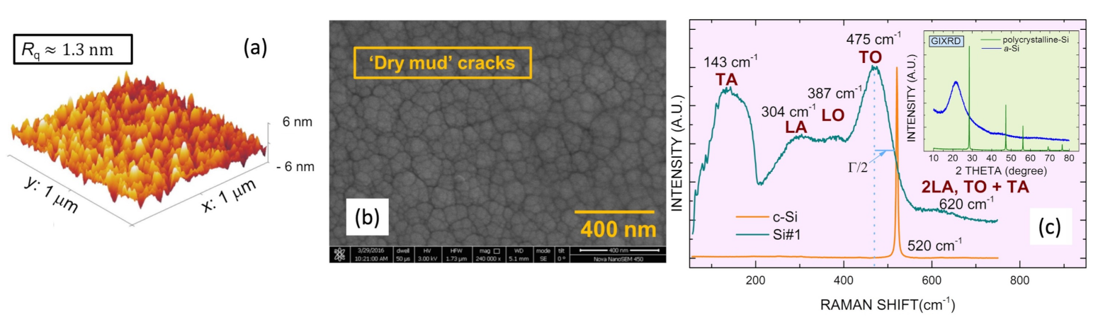
2.2. Surface, Structural and Optical Characterizations of the a-Si Films

The surface morphology, i.e., the root mean square value of the surface roughness, R q , of the a-Si films under study was examined by atomic force microscopy (AFM microscope, Bruker Multimode Nanoscope IIIA). The example AFM image shown in Figure 1a demonstrates that RFMS-a-Si samples have a reasonably smooth, shiny, and flat surface. AFM measurements indicate that the value of R q is approximately 1.3   n m ; on the other hand, the value of R q for the glass substrate employed was found to be around 0.60   n m .
It has also to be emphasized the surface effect, commonly described as ‘broccoli’, ‘orange peel’, or ‘dry mud’ cracks, observed in the top-view SEM micrograph (SEM: FEI Nova NanoSEM 450), corresponding to the representative RFMS-a-Si sample, Si#1, shown in Figure 1b. There is to date no clear explanation whatsoever of the possible mechanisms giving rise to the formation of this particular surface effect. Nevertheless, it may be suggested that it is related to the natural tendency of shrinkage of a thin coating layer, in order to diminish its surface energy, and would be caused by the tensile internal stresses in the films generated all of the them by the present RFMS-coating process.
Moreover, the refractive index, n, and the extinction coefficient, k, were determined from measurements of the normal-incidence optical transmittance spectra, exclusively. These optical spectra were collected by employing a Perkin-Elmer Lambda 1050 UV/visible/NIR, double-beam, ratio-recording spectrophotometer. The illuminated sample area was 10 m m × 1 m m , and the spectral slit width used was 2 n m ; the transmission data were measured with a data interval of 4 n m . All the transmission spectra were recorded over the wavelength range from 300 up to 2500 n m . Various different spots on each a-Si sample have been measured, and we have certainly found consistency between the results from the different spot-to-spot transmission measurements. Besides, the optically calculated film thickness was systematically cross-checked by cross-sectional SEM images, and additionally corroborated for some selected a-Si thin-film samples with a Veeco Dektak 150 mechanical surface profiler; it must be emphasized that the difference found with the average layer thickness obtained from the transmission spectrum only was, for all the cases studied, less than approximately 3.0 %.
In order to examine the atomic structure of the present sputtered samples, the first-order Raman spectra, recorded at room temperature, of the a-Si thin films investigated were excited with a 633 n m laser of 20 n W nominal power, by using a Horiba LabRAM HR Raman spectrometer. In Figure 1c, we display the Raman spectrum for the representative a-Si specimen, Si#1.
Let us start now with the interpretation of this measured Raman spectrum. Note that in a solid, a small part of an incoming photon energy can be used to excite a lattice vibration (phonon). The remaining energy escapes as a photon with slightly smaller energy compared to the incoming photon, and this energy shift is denoted as the Raman shift. In the case of a-Si solid, the momentum selection rule is relaxed, in comparison with the monocrystalline Si, and a variety of phonon modes and energies are permitted: A broad peak centered at around 480 c m 1 now almost dominates the whole Raman spectrum. It is observed that the Raman spectrum for the particular sample Si#1, shown in Figure 1c, exhibits a main peak at approximately 465 c m 1 , corresponding to the transverse-optic (TO) phonon band, and another main peak at about 152 c m 1 , belonging to the transverse-acoustic (TA) phonon band [16]. In addition to these two clearly dominant Raman peaks, two additional peaks associated with the longitudinal-optic (LO) phonon band, located at about 380 c m 1 , and with the longitudinal-acoustic (LA) phonon band, located at nearly 300 c m 1 , are also found. Moreover, note that the broad and small feature noticed at the high-energy side in the representative a-Si spectrum, illustrated in Figure 1c, at a value of the Raman shift of around 620 c m 1 , can be attributed to two plausible two-phonon excitations, such as TO + TA and 2LA, respectively [16].
The intensity of the TA-peak, I TA , taken with respect to the TO-peak intensity, I TO , is commonly interpreted as a degree of the extent of the intermediate range order within the atomic structure of the non-crystalline material. Thus, the larger the Raman–intensity ratio, γ Ram ( = I TA / I TO ) , the smaller the degree of intermediate-range order. The obtained value of the parameter γ Ram for the specimen of a-Si, Si#1, is found to be 0.89 ; the reported value of the γ Ram ratio for the sputtered (in this case, without magnetron enhancement) a-Si [17,18] is reported to be 0.80 . Orapunt et al. [19], on the other hand, prepared a novel form of a-Si by ultra-high-vacuum evaporation of Si atoms onto a room-temperature quartz substrate, with 98% of the mass density of the c-Si, and with a smaller value of the γ Ram ratio of 0.70 . Therefore, it is consequently concluded that our RFMS-a-Si samples are the most structurally-disordered of the previously considered and differently prepared forms of a-Si solid.
We can now undertake an indirect quantification of the bond-angle dispersion or structural disorder of the material, Δ θ , using the measured Raman spectra. Experiments and theory [20] clearly show that the transverse-optical TO band broadens as Δ θ (expressed in degrees) increases. The general relationship proposed by Beeman-Tsu [21] has the following form:
( Γ / 2 ) = A Raman + 3 Δ θ ,
with the parameter A Raman verifying that 7.5 c m 1 A Raman 12 c m 1 , and where ( Γ / 2 ) (in c m 1 ) is defined as the half-width at the high-energy side of the TO band (see Figure 1c). Therefore, the bond angle dispersion obtained in this case is found to be 15.0 degrees Δ θ 16.5 degrees, which can be consider a range of large values of Δ θ , indicating again the highly-disordered atomic structure of the RFMS-a-Si material under study.
Finally, the grazing incidence X-ray diffraction (GIXRD) measurements made on our a-Si samples corroborate, beyond any doubt, that these sputtered samples are fully amorphous, and none of the characteristic sharp X-ray diffraction peaks of its c-Si counterpart being evident, at all (these two clearly distinct diffraction patterns are shown in the inset of Figure 1c). The GIXRD and EDAX measurements performed also indicate the complete absence of impurities in the present RFMS-a-Si films.

3. Thin-Film Optics Theory and Model Dielectric Function

3.1. Some Basic Theoretical Considerations

Figure 2 displays the bi-layered specimen geometry, being made up of a weakly-absorbing layer of optical constants, n and k, on top of a transparent substrate. Thin-layer a-Si materials can be grown onto a thick substrate by using several physical or chemical vapor deposition techniques [22]. The investigated a-Si film has ideally a thickness, d. The glass substrate has smooth surfaces, and it is thick enough so that all the possible Fabry–Perot (FP) interference effects related to the non-absorbing glass substrate, totally disappear. The substrate refractive index, s, is independently obtained from normal-incidence transmittance measurements on the transparent substrate alone. This bi-layered sample is usually immersed in air with index of refraction n air = 1 .
The complex refractive index, n = n i k , of a thin layer is wavelength-dependent, or, in other words, optically dispersive. Its real part, n ( λ ) , is the refractive index, whereas its imaginary part, k ( λ ) , is the extinction coefficient, which accounts for the existing optical absorption of the semiconductor material. Furthermore, it is advisable to quantify such an absorption by the alternative absorption coefficient, α ( λ ) , and also by the dimensionless absorbance, x ( λ ) , which are both interrelated to the also dimensionless extinction coefficient by the equations, k ( λ ) = α ( λ ) λ / ( 4 π ) , and x ( λ ) = exp ( α ( λ ) d ) , respectively.
The model dielectric function, as a function of the photon energy, for non-crystalline materials, used in this study, is based upon both the Tauc joint density of states [23], and the Lorentz electron oscillator model [12]. The optical quantity to be now considered is the complex dielectric function, ϵ = ϵ 1 i ϵ 2 , and it should be mentioned that its dispersive real and imaginary parts are not independent, but, instead, they are correlated by the Kramers–Krönig (KK) equations [12]. For the present non-magnetic materials the interrelationships between the respective real and imaginary parts of this complex dielectric constant, ϵ , and the respective real and imaginary parts of its associated complex index of refraction, n , are given by
ϵ 1 = n 2 k 2 , ϵ 2 = 2 n k ,
or equivalently expressed,
n = 1 2 ϵ 1 2 + ϵ 2 2 + ϵ 1 , k = 1 2 ϵ 1 2 + ϵ 2 2 ϵ 1 .

3.2. Spectral Transmittance for a Nonuniform Semiconductor Film onto a Transparent Glass Substrate

Let us first consider the normal-incidence monochromatic light illumination on the ideal surface of a uniform semiconductor thin layer, grown onto a thick transparent glass substrate, as illustrated in Figure 2a. Taking into consideration the infinite reflections occurring at the three existing interfaces between the three constituent media of this particular optical system: air–layer, layer–substrate, and substrate–air, respectively, it is found that the spectral transmittance is given by the exact expression [14,24,25] (we present here again these already reported formulae for the sake of self-completeness of the present manuscript),
T uniform ( λ ; n , k , s , d ) = A x B + x C sin φ D cos φ + E x 2 ,
where
A = 16 ( n 2 + k 2 ) s , B = ( n + 1 ) 2 + k 2 ( n + 1 ) ( n + s 2 ) + k 2 , C = 2 k 2 ( n 2 + k 2 s 2 ) + ( n 2 + k 2 1 ) ( s 2 + 1 ) , D = 2 ( n 2 + k 2 1 ) ( n 2 + k 2 s 2 ) 2 k 2 ( s 2 + 1 ) ( n 1 ) ( n s 2 ) + k 2 , E = ( n 1 ) 2 + k 2 , φ = 4 π n d / λ .
In addition, in the spectral range corresponding to the strong optical absorption within the thin film, where the FP interference pattern starts disappearing, the spectral transmittance formula basically depends only on the exponential term appearing in the numerator of such equation. Therefore, in this specific spectral range of high absorption, the previous exact formula of the transmittance is reasonably approximated as follows:
T approx ( λ ; n , k , s , d ) A x B 16 n 2 s x ( n + 1 ) 3 ( n + s 2 )
The thickness of an idealized perfect layer is certainly constant, but in a real specimen, this is rarely the situation, and, thus, significant thickness nonuniformity and/or surface roughness are often present in these real thin-film samples. The necessary simplifying assumption to be made in order to model the geometry of a real nonuniform thin layer will be to suppose such a layer, having a wedge-shaped profile as that depicted in Figure 2b. In order to be able to determine this film-thickness variation through the light spot, a homogeneity or wedging parameter, Δ d , is introduced, and also its associated average film thickness, d ¯ , in such a way that the actual layer thickness in the illuminated area of the sample increases linearly from a minimum value of d = d ¯ Δ d , up to a maximum value of d = d ¯ + Δ d (see Figure 2b).
Under this proposed working hypothesis of a linear dependence of the variable layer thickness through the spectrophotometer light spot, a much more realistic and accurate expression for the transmission, accounting for its varying thickness, will be derived by integrating upon the two optical variables which depend upon the variable thickness, that is, the optical phase, φ , and the absorbance, x, both previously introduced in Equation (5). Nevertheless, the influence of the variable thickness upon the absorbance is clearly negligible, as compared with the much stronger influence of the variable thickness upon the phase. Taking into account this suggested simplification, the integral for the transmittance will then be written as follows:
T Δ d non - uniform ( λ ; n , k , s , d ¯ , Δ d ) =
φ 1 φ 2 d φ φ 2 φ 1 x 1 x 2 d x x 2 x 1 A x B + C sin φ D cos φ x + E x 2
1 φ 2 φ 1 φ 1 φ 2 A x B + C sin φ D cos φ x + E x 2 d φ ,
with
x 1 = exp α ( d ¯ Δ d ) , x 2 = exp α ( d ¯ + Δ d ) , φ 1 = 4 π n ( d ¯ Δ d ) / λ , φ 2 = 4 π n ( d ¯ + Δ d ) / λ .
Note that the analytical integration of Equation (7) gives rise to inverse hyperbolic functions; it is indeed a complex expression, derived in the present study by employing the useful tool of Mathematica software system (version 12.3), and it is now expressed after doing various algebraic manipulations [25],
T Δ d hyper ( λ ; n , k , s , d ¯ , Δ d ) = 2 A x ( φ 2 φ 1 ) H tanh 1 G H tanh 1 F H ,
where
F = x C + B ( D + E x ) tan ( φ 1 / 2 ) , G = x C + B ( D + E x ) tan ( φ 2 / 2 ) , H = B 2 x 2 C 2 + D 2 2 B E E 2 x 2 .
It is convenient next to express the spectral transmittance for the layer-on-substrate specimen, using angle or circular functions, instead of the previously employed hyperbolic functions, for reasons that later will be absolutely evident. Again, after some additional algebraic manipulations, a more compacted expression for the transmittance is derived,
T Δ d uncorrected ( λ ; n , k , s , d ¯ , Δ d ) = 2 A x ( φ 2 φ 1 ) H tan 1 G H tan 1 F H .
It has to be stressed that Equation (11), unfortunately, cannot be yet used in the optical characterization of real semiconducting thin layers, by only using the transmission spectrum. The existence of a multi-valued inverse goniometric function in Equation (11) is the cause of the presence of discontinuities around the minima of the transmission spectrum if the necessary correcting angles, multiples of π radians, are not correctly introduced. The existence of such discontinuities in the transmittance expression makes Equation (11) certainly useless for our final purpose.
All of these invalidating effects corresponding to the expression of the transmission are clearly evidenced in Figure 3, where such a previous mathematical expression is graphed for a hypothesized hydrogenated a-Si thin film, whose homogeneity parameter Δ d has the proposed exact value of Δ d = 30 n m , with a typical average thickness, d ¯ = 1500 n m , a plotted wavelength range λ = 500–900 n m , and, finally, with the optical constants given by the two following semiempirical dispersion relationships [24], with the wavelength in n m ,
n a - Si : H ( λ ) = 2.60 + 3.0 × 10 5 λ 2 , k a - Si : H ( λ ) = λ 4 π 10 ( 1.5 × 10 6 / λ 2 ) 8 .
The refractive index of the non-absorbing glass substrate is assumed to be for this simulation s = 1.51 = constant. It is further noticed in Figure 3 that the uncorrected transmittance curve of the gedanken film completely matches the corresponding numerical integration of Equation (11), except around the minima of the transmission curve, as was already referred to above.

3.3. Optical Phase Change: Correcting Integer Numbers N c , 1 and N c , 2

The two parameters F and G in Equation (10) do contain circular functions, whose two respective arguments φ 1 and φ 2 are expressed by Equation (8). Depending on the values of n, k, d ¯ , Δ d , and λ , the corresponding argument of the angle functions could exceed the critical value of 2 π radians. Taking into account the fact that those two parameters F and G, are within inverse goniometric functions, it is, thereby, necessary to properly evaluate the exact number of multiples of 2 π radians summed up to the corresponding optical phase, φ , within the thin layer. This newly proposed key step will, indeed, suppress the above-mentioned completely invalidating discontinuities in the transmission spectrum.
In order to account for the strong influence of the layer thickness nonuniformity upon the spectral transmittance, we now suggest the introduction of two absolutely necessary correcting integer numbers, N c , 1 and N c , 2 , respectively, into Equation (11), in order to be able to properly evaluate the optical-phase change taking place within the thin film. Therefore, the corrected equation of the spectral transmittance for a real, non-uniform layer is finally derived:
T Δ d corrected ( λ ; n , k , s , d ¯ , Δ d ) = 2 A x tan 1 G H + N c , 2 π tan 1 F H + N c , 1 π ( φ 2 φ 1 ) H ,
where the two new correcting integer numbers, N c , 1 and N c , 2 , respectively, are now given by the two following expressions:
N c , 1 = round φ 1 / 2 π , N c , 2 = round φ 2 / 2 π .
This defined function ’round’ does round off the argument to its closest integer value, and it is totally equivalent to the function with the same name, implemented in the mathematical software system Matlab (R2021a), which will be largely used later. The novel corrected Equation (13) presented in this work, very importantly, is a continuous function that can be used in order to optically characterize an ample variety of thin-film amorphous semiconductors, with high accuracy. Moreover, the so-far existing limiting maximum value for the wedging parameter, Δ d ( = λ / 4 n ) , when optically characterizing strongly wedge-shaped layers, has been fortunately successfully suppressed with the introduction of the appropriate correcting numbers, N c , 1 and N c , 2 , in the expression of the corrected spectral transmittance, T Δ d corrected .
It should be added that the physical importance of Equation (13) is based upon the fact that the whole normal-incidence transmittance spectra of wedge-shaped semiconducting thin films, can be evaluated by using the ’inverse-synthesis method’ proposed by Dobrowolski et al. [26], rather than the dispersion model-free characterization method, based exclusively upon the use of the upper and lower envelopes of the spectral transmittance, making use of only a portion of the transmission spectrum. In addition, the obliged exclusion for optical characterization purposes of nonuniform layers having a value of Δ d > λ / 4 n [27], is now, with the presented novel formulae, fully eliminated.

3.4. Determination of the Optical Constants by Applying the TLUC Dispersion Model

The glass substrate onto which the a-Si thin layer was deposited was previously checked for transparency in the complete wavelength region analyzed and, therefore, completely characterized from the optical standpoint by only its real refractive index, s (knowing that k s 0 ). This optical parameter has been obtained from independent normal-incidence transmission measurements on the bare transparent glass substrate, and by making use of the well-known expression for the transmittance of a non-absorbing slab, T s [24]:
T s ( λ ) = 2 s s 2 + 1 ,
So, by solving for s we get
s ( λ ) = 1 T s + 1 T s 2 1 .
The KK-consistent optical dispersion model that is adopted in this study is the Tauc–Lorentz–Urbach-Continuous parameterization, as suggested by Foldyna et al. [28]. This TLUC dispersion model was found to be appropriate for amorphous semiconductors in general, and is a realistic generalization of the very popular Tauc–Lorentz (TL) parametrization proposed by Jellison and Modine [29,30], with the certainly existing exponential Urbach band tail being added to the TL model. Thus, the more complete TLUC model employs six free-adjusting parameters: A mp , E 0 , C br , E g , E c , and ϵ 1 ( ) ; that is, interestingly just only one more parameter than in the case of the TL model, specifically that one associated to the Urbach absorption tail spectral region, E c .
The imaginary part of the complex dielectric constant, ϵ 2 ( E ) , in this TLUC parameterization is now given as a piecewise function:
ϵ 2 ( E ) = 1 E A mp E 0 C br ( E E g ) 2 ( E 2 E 0 2 ) 2 + C br 2 E 2 , E E c , ϵ 2 ( E ) = A u E exp E E u , 0 E < E c ,
where the first expression of ϵ 2 ( E ) , for values of E E c , is identical to that corresponding to the TL parameterization, and the second expression of ϵ 2 ( E ) , for 0 E < E c , indicates the contribution of the exponential Urbach band tail. In particular, the four free-fitting parameters E g , A mp , E 0 , and C br stand for the optical band-gap energy, the Lorentz-oscillator amplitude, the Lorentz-oscillator peak energy, and the broadening parameter or single-oscillator width, respectively.
Furthermore, the two additional TLUC model parameters A u and E u , the so-called Urbach amplitude and energy, respectively, have been added in order to guarantee the continuity of the imaginary part of the complex model dielectric function, and also its first derivative, and for that particular reason the model has been labeled ’continuous’. These two Urbach tail parameters are expressed this way,
E u = E c E g 2 2 E c ( E c E g ) C br 2 + 2 ( E c 2 E 0 2 ) C br 2 E c 2 + ( E c 2 E 0 2 ) 2 , A u = exp E c E u A mp E 0 C br ( E c E g ) 2 ( E c 2 E 0 2 ) 2 + C br 2 E c 2 .
The real part of the complex dielectric function, ϵ 1 ( E ) , is now derived by employing the analytical integration associated with the fundamental KK relations between ϵ 1 ( E ) and ϵ 2 ( E ) . Thus, we can write next this real part of the complex dielectric constant as follows:
ϵ 1 ( E ) = ϵ 1 ( ) + 2 π P 0 ξ ϵ 2 ( E ) ξ 2 E 2 d ξ ,
where P denotes the Cauchy Principal value of the integral. In this fashion, we find
ϵ 1 ( E ) = ϵ 1 ( ) + ϵ 1 , TL ( E ) + ϵ 1 , UT ( E ) ,
where the contribution of the TL model to the TLUC model dielectric function, for E c E < , is expressed by the following equation, given here again for the sake of self-completeness of the present paper:
ϵ 1 , TL ( E ) = A mp E 0 C br E 2 + E g 2 π σ 4 E ln | E c E | E c + E + 2 A mp E 0 C br E g π σ 4 ln | E c E | ( E c + E ) E 0 2 E c 2 2 + C br 2 E c 2 +
+ A mp C br a L 2 π σ 4 α E 0 ln E 0 2 + E c 2 + α E c E 0 2 + E c 2 α E c A mp a A π σ 4 E 0 π tan 1 2 E c + α C br tan 1 2 E c α C br +
+ 4 A mp E 0 E g E 2 γ 2 π σ 4 α π 2 tan 1 2 ( E c 2 γ 2 ) α C br ,
and where the intermediate variables previously introduced in the above equations are also given by the next expressions:
a L = ( E g 2 E 0 2 ) E 2 + E g 2 C br 2 E 0 2 ( E 0 2 + 3 E g 2 ) , a A = ( E 2 E 0 2 ) ( E 0 2 + E g 2 ) + E g 2 C br 2 , γ = E 0 2 C br 2 / 2 , α = 4 E 0 2 C br 2 , σ 4 = ( E 2 E 0 2 ) 2 + C br 2 E 2 .
Additionally, the Urbach band tail part of the model dielectric function, for 0 < E < E c , is written in this way,
ϵ 1 , UT ( E ) = A u E π { exp E E u Ei E E u Ei E c + E E u
+ exp E E u Ei E c E E u Ei E E u }
where the introduced function ‘ E i ( x ) ’ is the so-called ‘generalized exponential integral function’, as also implemented as a Matlab function, with exactly the same name, in the Matlab software used in this work, in such a fashion that
Ei ( x ) = P x exp ( t ) t d t .

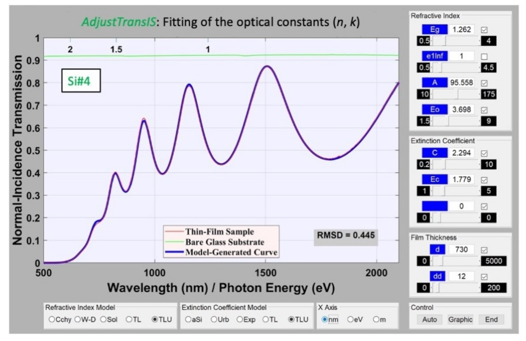
3.5. ‘AdjustTransIS’: Matlab Computational Program for Optical Characterization of Amorphous Semiconductor Films

The computational program named ‘AdjustTransIS’, created in order to perform the accurate optical characterization of non-uniform semiconductor thin layers, was coded in Matlab and falls into the category of reverse-engineering, or inverse-synthesis method. The simplified flowchart of its algorithm was already presented in [31], and it ought to be noted that is fully configurable by the use of MS-Excel files. The Matlab toolbox developed is able to quickly fit a model-generated transmittance spectrum to the experimentally measured transmittance spectrum of a wedge-shaped semiconductor layer, by fitting up to a maximum number of nine free-adjusting model parameters. Up to seven of them associated with the implemented dispersion relations, plus two nonuniform film geometrical parameters, namely, the average film thickness and, interestingly, the homogeneity parameter, d ¯ and Δ d , respectively.
The very basic idea behind ‘AdjustTransIS’, in order to accurately compute the TLUC-model parameters, is to calculate the set of values minimizing the figure-of-merit (FOM) metrics that follows,
FOM = 100 × RMSE = 100 × i = 1 N ( T i , meas T i , simu ) 2 N ,
where N stands for the total number of experimentally measured data points, T i , meas denotes the as-measured value of transmission, and T i , simu the corresponding TLUC model-generated value of transmission, for those particular wavelengths for which the glass substrate employed is non-absorbing. The chosen FOM metrics in order to be minimized is 100 times the root mean square error (RMSE) associated with the differences between the measured and simulated transmission data, that is, the square root of the average of the squared transmission differences, or residues. In the Matlab-coded program ‘AdjustTransIS’, the minimization routine employed was the Nelder–Mead (downhill) simplex algorithm, incorporated into a specific Matlab function. This is a nonlinear, direct search method, implemented in Matlab by its corresponding ’fminsearch’ function, and it was adopted in order to compute the minimum of an unconstrained multivariable function.

4. Results and Discussion

4.1. Computation of the Optical Properties by ‘AdjustTransIS’

The as-measured transmittance spectra for the RFMS-a-Si samples studied were all analyzed by the Matlab-coded program ‘AdjustTransIS’, and in Table 1 all the best-fit parameters belonging to the TLUC model used, obtained from two representative spectra, are listed. Figure 4a,b displays the comparison between the simulated and experimental transmittance spectra for the corresponding two representative a-Si samples, Si#1 and Si#2. The difference between the simulated and measured data, Δ T = T simu T meas , in the particular case of sample Si#1, is also plotted in Figure 4a. It is seen the remarkable agreement between the two generate and experimental transmittance spectra, with a very low value of FOM of 0.421, in the specific case of Si#1; a value slightly larger of the FOM of 0.565 has been found for the sample Si#2. For the sake of clarity, the x-axis of all the graphs represents photon energy, instead of vacuum wavelength, as given initially by the spectrophotometer, when plotting the transmission curves, and we have also employed open circles instead of solid lines, in order to plot the transmission data for these two representative a-Si specimens, Si#1 and Si#2, respectively.
In addition, in order to clearly show the effectiveness and ease of use of the detailed-designed Matlab-based GUI (i.e., the graphical user interface or main window) of the toolbox ‘AdjustTransIS’, showing the representative values of all the free-adjusting and fixed parameters, associated with the simultaneous optical and geometrical characterizations, corresponding to the transmittance spectrum for the particular a-Si specimens Si#3 and Si#4, is displayed in the Appendix A. The full information regarding the free and fixed TLUC-model parameters was notified by convenient checkboxes. Furthermore, by using the appropriate radio buttons, we choose the TLUC parametrization selected in this work. The very low value of the FOM found for these other representative specimens analyzed, Si#3 and Si#4, of 0.445 and 0.446, respectively (see the Figure A1 in the Appendix A), have again unambiguously demonstrated the excellent fit between the experimental and simulated transmission data for the samples under investigation.
The computed complex refractive indices of the two RFMS-a-Si samples, Si#1 and Si#2, as a function of wavelength, are illustrated in Figure 5. The average thickness of the particular wedge-shaped specimen Si#1 was 770 n m , and its corresponding non-zero thickness variation was 25 n m . It should be stressed that this lack of film-thickness uniformity represents a percentage of 3.2 % of the calculated average layer thickness. Note that this particular result shows the great capability of the proposed optical characterization approach, highly sensible to the lack of parallelism between the faces of the thin-layer material, and based uniquely upon the shrunk transmittance spectrum of the non-homogeneous a-Si layer.
Continuing with the analysis of the optical properties of RFMS-a-Si, it is observed in Figure 5 that in the range of very low wavelengths, very close to zero, n is a decreasing function of the wavelength (i.e., d n / d λ < 0 ). The optical dispersion is then called normal dispersion. For values of the wavelength larger than approximately 100 n m , the refractive index starts increasing, instead, with increasing wavelength (i.e., d n / d λ > 0 ), and it is then called the regime of ’anomalous’ dispersion. For wavelength values higher than 425 n m , covering now the whole visible spectral range, the regime of normal optical dispersion is again observed. From the KK relationships, the obtained wavelength dependence of the refractive index has to be necessarily correlated to the existing optical absorption of the a-Si layer, clearly shown by the behavior of its extinction coefficient, k (see Figure 5). There is, as expected, a noticeable narrow absorption band around the specific wavelength value of nearly 287 n m .
The best-fit single-TLUC oscillator parameters for the two representative layers, Si#1 and Si#2, respectively, indicated in Table 1, are next discussed. For these two specific cases, the amplitude of the TLUC oscillator A mp is approximately 99 e V , and the optical band gap value E g is nearly 1.19   e V . The values of the other three TLUC parameters E 0 , C br , and E c , are around 3.73   e V , 2.40   e V , and 1.75   e V , respectively. Furthermore, following Ferlauto et al. [33], and also Foldyna et al. [28], the corresponding offset parameter, ϵ 1 ( ) , has been always reasonable and successfully fixed to 1. Note at this point of the discussion that, in the present physical interpretation of the experimental results, the concept of energy band gap, E g , is still maintained, even in the absence of crystallinity (there is no long-range order in the atomic structure) of the studied amorphous semiconductor material, through the existing influence of the preserved short-range ordering in the atomic structure of pure a-Si, upon its electronic density of states.
The values of the Urbach energy and amplitude parameters, E u and A u , respectively, determined from the previous TLUC parameters, are also listed in Table 1, for the two representative transmittance spectra analyzed. For the sake of comparison and greater completeness, we have added to Table 1 the values of the TLUC-parameters found for two more RFMS-a-Si samples, Si#3 and Si#4, respectively. The values of the so-called Tauc gap, E g , Tauc , all also computed by applying the Matlab program ‘AdjustTransIS’ (it will be discussed in detail below), are also shown in Table 1. The reproducibility of the properties of RFMS a-Si films depends on the sputtering parameters having the required time stability, which is actually difficult to assure due to the complexity of the non-equilibrium deposition process. This could justify the relative small differences found, lower than about 4.0 % (beyond the unavoidable statistical fluctuations), in the values of the TLUC parameters corresponding to the four metastable a-Si samples listed in Table 1. Moreover, the calculated value of the refractive index at the particular NIR wavelength of 2500 n m , n ( 2500 ) , approximately 3.164 , and the two alternative iso-absorption gaps, E 03 , and E 04 (the values of energy corresponding to the values of α of 10 3 cm 1 and 10 4 cm 1 , respectively), are clearly marked in Figure 5 and Figure 7, respectively.
Our computed TLUC parameters are consistent with those reported by some of the authors of this paper, in a previous work concerning with the study of a-Si semiconducting material, by the VASE technique [34]. Moreover, they are also comparable with the best-fit values of the TL-parameters, calculated from the evaporated amorphous silicon (e-a-Si) data compiled in the Palik’s Handbook of Optical Properties [35], by Jellison and Modine [29]. Furthermore, note that Foldyna et al. [28] found a value of the band gap energy of 1.19   e V , as a result of applying its TLUC model to previous data belonging to e-a-Si, reported in the mentioned Palik’s Handbook. This particular value of the optical gap of 1.19   e V , interestingly, is coincident with the value of E g reported by Jellison and Modine (see Table 1), employing its limited TL parametrization, instead (it must be stressed that without the inclusion of the contribution of the Urbach absorption tail), to the same set of Palik’s compiled optical data for e-a-Si. It has finally to be noted that the value of E g calculated for the two representative samples Si#1 and Si#2, respectively, is, in both cases, exactly the value of 1.19   e V (see Table 1), in perfect agreement with the above-mentioned value of the optical gap reported in the literature.

4.2. Comparison with the Transmission Data Analysis by the Swanepoel Envelope Method

The complex refractive index, n , was also determined by the alternate transmission envelope method proposed by Swanepoel [24,27], by using our transmittance data from the weak-to-medium absorption region. The envelope method is relatively simple and, importantly, does not require assuming a dispersion model prior to the transmission data analysis, on the contrary to the inverse synthesis method. The basic principle of this method is to accurately draw the two top and bottom envelope curves, that are tangential interpolation curves between the interference maximum points, and between the interference minimum points, respectively. At those tangential points, the average film thickness, d ¯ , the real refractive index, n, and the respective tangential wavelength, λ tan , are related by the interference equation:
2 n ( λ tan ) d ¯ = m λ tan ,
where m is the interference order number, which is an exact integer for top tangential points, and an exact half-integer for bottom tangential points (see Figure 3).
In this work, this envelope method is also used in order to calculate n and k, in the transparent-to-medium absorbing region, where the photon energy is correspondingly around or below the optical band-gap. From the transmittance spectra displayed in Figure 4, one can expect in the strong absorption region that the two upper and lower envelope curves merge into one single curve. Thus, it is not possible to find the optical constants, n and k, in this spectral range of high absorption, without assuming a particular dispersion model for the refractive index. Furthermore, for a sufficiently thin layer ( d ¯ 100   n m ) that has very few (or none of them) peaks and valleys, the interpolation is certainly inaccurate, but fortunately it is not at all the case in the present spectra. Instead, we have been able to make reliable interpolations between the tangential points because our a-Si layers are certainly thick enough. The two top and bottom envelopes have been smoothly constructed by the useful algorithm suggested by Minkov et al. [36,37].
After computer generating the two envelopes of the transmission spectrum, the refractive index, the extinction coefficient, the average layer thickness, and the homogeneity parameter have been calculated by using the dispersion model-free Swanepoel method, described in detail in [38,39,40,41,42,43]. Particularly, it must be emphasized that the differences between the values of d ¯ and Δ d , determined by the envelope method and by inverse synthesis, respectively, are, in all the samples analyzed in this study, smaller than 1.0 %; especially remarkable is the fact that the values of the thickness variation Δ d for the tapered layer Si#1, calculated by the two different approaches, are coincident, within our range of accuracy. It is found that Δ d = 25 n m with both methods, and as indicated before, it represents approximately the 3.2 % of the value of d ¯ . Besides, the values of d ¯ calculated by the TLUC parametrization and the Swanepoel method are, indeed, fairly close to the cross-checking film-thickness values directly measured by cross-sectional of SEM microscopy images, d SEM s , listed in Table 1. Superimposed as two insets to Figure 4a,b are displayed the respective two cross-sectional SEM images, belonging each of them to a representative a-Si sample, along with the comparison of the two generated and measured transmission spectra corresponding to each one of the specimens. The directly measured values of d SEM are 777 n m and 1112 n m for the specimens, Si#1 and Si#2, respectively, which are remarkably near to their optically calculated values of d ¯ . The values of the two optical constants n and k obtained by using the transmission envelope method in the allowed photon energy range of about 0.62–1.8 eV, and those from TLUC model fit, in the whole measured spectral range, are very close too, as shown in Figure 5.

4.3. Wemple–DiDomenico Framework: Insight into Material Porosity

The TLUC model yielded sub-gap n-values, and those other data for the refractive index dispersion independently calculated by the model-free envelope method, were systematically analyzed by using the Wemple–DiDomenico (WDD) single effective oscillator model [44,45]. These authors thoroughly investigated optical-dispersion data below the band gap for more than a hundred diverse materials, both covalent and ionic, and both crystalline and amorphous. They found that the whole set of dispersion data examined can be fitted, to an excellent approximation, by the following relationship:
ϵ 1 ( ω ) = n 2 ( ω ) = 1 + E so E d E so 2 ( ω ) 2 ,
where ω is the photon energy, E so is the single-oscillator energy, and E d is the single-oscillator strength or dispersion energy. Therefore, plotting ( n 2 1 ) 1 vs. ( ω ) 2 lets us determine the two single-oscillator parameters, E so and E d , respectively, by fitting a linear function to the set of calculated values of the refractive index. The WDD plots for the two representative RFMS-a-Si samples Si#1 and Si#2, respectively, are shown in Figure 6. The obtained values of the WDD single-oscillator parameters E so and E d are presented in Table 2. Mention must be made that departures from the linear behavior in the WDD plots, at larger photon energies, very often reported in the literature [44,45], and being explained by the result of the proximity of the band edge (that is, the interband transitions), have not been observed in any of the present RFMS-a-Si specimens.
The extrapolated values of the static refractive index, n ( w = 0 ) , for the representative a-Si samples are also listed in Table 2.
Interestingly, a value of the TL model-yielded E d parameter for dense and fully amorphous, self-implanted (i.e., non-hydrogenated) a-Si of 36.4   e V , reported by Chen and Shen [46], that was, in turn, calculated from the values previously reported by Adachi and Mori [32,47] of the complex dielectric constant, being this measured by the VASE technique, has been found in the literature. This result demonstrated that the popular literature data used a reference of ’dense’ a-Si, measured by Bagley et al. [48,49], is actually influenced by the contribution of an existing component of microcrystalline Si, whose volume fraction was estimated to be, surprisingly, about 53%. It should be pointed out that the reference values of E so and n ( 0 ) reported by Chen and Shen [46] and, also, corroborated by us, for that Si-ion-implanted a-Si layer, are 2.87   e V and 3.697   e V , respectively.
The dispersion energy, E d , measures the average strength of the interband electronic transitions, and obeys the widely-applicable empirical rule, expressed as follows [44,45]:
E d = β N c Z a N e ( ρ a / ρ x ) , ( E d in eV units ) ,
where β c =   0.37 ± 0.04   e V , in the case of ’covalent’ materials, and β i =   0.26 ± 0.03   e V , in the case of the more ’ionic’ materials. In Equation (28), N c stands for the coordination number of the cation, that is, the nearest neighbor to the anion; Z a denotes the formal chemical valency of the anion ( Z a = 4, for Si); N e is the total number of valence electrons, where the cores are excluded, per anion ( N e = 8 ); and, last, ρ a / ρ x is the ratio of the mass density of the amorphous material to the mass density of its crystalline counterpart, with its ’compacted’ and well-ordered atomic structure, instead.
This mass–density ratio, ρ a / ρ x , in Equation (28) is indeed the key factor in determining the refractive-index behavior of the studied RFMS-a-Si films. Therefore, we assume that E d decreases linearly with the increase of the volume fraction of interconnected voids, i.e., the porosity, within the underdense a-Si layers; it must be also noted that E d scales with the volume density of valence electrons in the material, involved in the transition at the single-oscillator energy of E so . We have thereby used the already mentioned particular value of the dispersion energy, E d , of 36.4 eV for the dense, or pore- or void-free, self-implanted a-Si material, obtained, in turn, from the data found by Adachi and Mori [32,47], as the correct reference value of E d in order to be compared with. Therefore, we can express mathematically all those previously-proposed simplifying ideas about the calculation of the WDD void volume fraction, f void WDD , from the calculated values of E d , by the simple approximate formula:
E d underdense = E d dense 1 f void WDD ,
and, by solving for f void WDD , we derive the following expression:
f void WDD = 1 E d underdense E d dense .
Finally, by using this approximate relation, the values of f void WDD for the representative underdense RFMS-a-Si samples were obtained from the calculated values of the WDD parameter, E d , and are indicated in Table 2.

4.4. Bruggeman Effective Medium Approximation: Alternate Void-Volume-Fraction Determination

An additional cross-checking determination of the void volume fraction, f void Bru , for the RFMS-a-Si thin layers under investigation, by using the self-consistent Bruggeman effective medium approximation (B-EMA) [49,50], and the values of the complex dielectric function, ϵ , calculated by the extrapolation of the WDD dispersion formula to zero photon energy, ϵ ( 0 ) = 1 + E d / E so , is next carried out.
According to this B-EMA approximation, a mixture of diverse materials can be considered as a homogeneous medium, possessing an effective complex dielectric constant, ϵ eff , that can be obtained from the individual complex dielectric constants, ϵ i ’s, and the respective volume fractions, f i ’s, of the individual constituent components, whereas it is obeyed that i f i = 1 . Following the B-EMA approach, for a composite material of the various i-components, the following equation is verified:
i f i ϵ i ϵ eff ϵ i + 2 ϵ eff = 0
By using the basic relation between the complex dielectric constant and the complex refractive index, ϵ = n 2 , and by also taking into account the two constituent components of our a-Si thin-film material, whose volume fractions are 1 f void Bru (for the dense or pore- or void-free a-Si), and f void Bru (for the air-filled pores or voids), respectively, along with setting, n eff n underdense ( 0 ) , we can express Equation (31) as
( 1 f void Bru ) n dense 2 ( 0 ) n underdense 2 ( 0 ) n dense 2 ( 0 ) + 2 n underdense 2 ( 0 ) + f void Bru 1 n underdense 2 ( 0 ) 1 + 2 n underdense 2 ( 0 ) = 0 .
Hence, by solving for f void Bru , we have the final formula:
f void Bru = ( 1 + 2 n underdense 2 ( 0 ) ) ( n dense 2 ( 0 ) n underdense 2 ( 0 ) ) 3 n underdense 2 ( 0 ) ( n dense 2 ( 0 ) 1 ) .
The two necessary values of the refractive index, that is, the value of n ( 0 ) for the dense, self-implanted a-Si, n dense ( 0 ) = 3.697 , and the value of the refractive index for air, n air = 1 , are now inserted in the previous Equation (33). The calculated values of B-EMA-based void volume fraction, f void Bru , are listed in Table 2. Note that the two respective values of the void volume fraction, f void WDD and f void Bru , obtained by two different approaches, for our RFMS-a-Si specimens, are practically identical; the value of the porosity for the specific rf-magnetron sputtering deposition conditions employed in this work, with an Ar-pressure of about 4.4 Pa, is found to be approximately 21%. Karabacak and Demirkan [9] have reported values of the porosity for their sputter-deposited a-Si films produced at different Ar-gas pressures, as high as approximately 30%, corresponding to a mass density of 1.64   g / c m 3 . Their reported void fractions as a function of working pressure are absolutely consistent with our obtained value of about 21%, which is surprisingly much higher than the reference value found for ion-implanted a-Si of around 3.0%.

4.5. Absorption Edge and Dielectric Function of RFMS-a-Si

In Figure 7, we plot the optical absorption coefficient, as a function of photon energy, of the two representative RFMS-a-Si samples, Si#1 and Si#2. From these optical absorption edges shown in Figure 7, the corresponding two iso-absorption gaps, E 03 and E 04 , respectively, for each representative sample, are now determined. The value of the gap parameter, E 04 , is generally found to be around 0.15 0.30   e V larger than the value of the Tauc gap, E g , Tauc , for Si-based non-crystalline materials. In the present a-Si films, the difference between the obtained value of the iso-absorption gap E 04 and the fitted value of the optical gap, E 04 E g , has been found to be approximately 0.28   e V , well within the previous gap-difference range. This gap difference, E 04 E g , has been attributed to the width of the conduction-band tail, and, therefore, to the contribution associated with the electron states localized in the mobility pseudo-gap of the a-Si material. It is generally argued that the larger the structural randomness within the amorphous material, the wider its conduction band tail.
The exponential dependence of the absorption coefficient, α , of the form α ( ω ) = α 0 exp ( ω / E u ) , the well-known Urbach region equation, is clearly obeyed, as shown in Figure 7. The computed values of the Urbach energy parameter, E u , listed in Table 1, were found to be about 250 meV, in all the samples under study. This very large value of the parameter E u is indicative of the high degree of structural disorder of the present non-crystalline material, fully consistent with was above inferred from both X-ray diffraction and Raman spectroscopy measurements. The maximum value of α , α max , found at the specific value of the photon energy of nearly 5.0   e V is 1.42 × 10 6 cm 1 (see Figure 8).
Next, the real and imaginary parts, ϵ 1 and ϵ 2 , respectively, of the complex dielectric constant, ϵ , as a function of the photon energy, for the two representative a-Si samples, Si#1 and Si#2, are shown in Figure 8. Note that the broad peak of the imaginary part of the dielectric function, ϵ 2 , whose highest value, ϵ 2 , max , is associated with the splitting of bonding and antibonding electron states, and it is located at an energy position, E ( ϵ 2 , max ) , of nearly 3.71   e V (see Table 2), almost coincident with the calculated value of the TLUC parameter E 0 . This single smeared peak of ϵ 2 is usually shown by tetrahedrally bonded amorphous semiconductors [34], like the cases of elemental Si and Ge.
Generally speaking, the amorphous material exhibiting the largest value of ϵ 2 , max (see Figure 8), is regarded as that belonging to ‘intrinsic’, dense, hydrogen-less, and fully amorphous silicon; i.e., the self-implanted a-Si, with the above-mentioned highest value of the WDD dispersion energy, E d , of 36.4 eV. The largest value of the ϵ 2 , max of 26.6 for this particular H-free a-Si material, measured by Adachi and Mori [32,47], and based upon VASE measurements, at a value of the photon energy, E ( ϵ 2 , max ) , of 3.45   e V , must necessarily be the reference value in order to be compared with. Hence, the significantly lower value of the amplitude of the ϵ 2 peak for the case of our RFMS-a-Si samples can plausibly be explained by their proportionally lower mass density, attributed to their inherent micro-voided structure, under the present growth conditions.
The experimental ϵ 1 ( E ) and ϵ 2 ( E ) spectra of c-Si [49] are also displayed in Figure 8 by dashed lines. The prominent critical point (CP) features seen in these two ϵ 1 ( E ) and ϵ 2 ( E ) spectra of c-Si are the E 1 and E 2 structures at E approximately 3.4 and 4.3 eV, respectively. The disappearance of the CP features in the amorphous material is due to the breakdown of the crystal periodicity in the amorphous material. The comparative experimental n ( λ ) and k ( λ ) spectra of c-Si shown in Figure 5, on the other hand, have been directly obtained from those previous ϵ 1 ( E ) and ϵ 2 ( E ) spectra of c-Si reported by Aspnes [49].

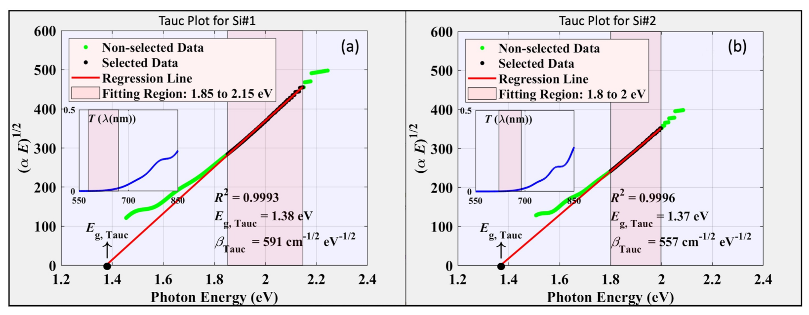
4.6. Determination of the Band-Gap Energy by Tauc’s Extrapolation Method

The absorption coefficient was also independently obtained directly from a portion of the transmission spectrum, by using only the spectral region of high absorption of such a spectrum, where the FP interference fringes start disappearing (see Figure 4 and the inset of Figure 9). Therefore, for those large values of α , α free ’s, where the absorbance obeys that x 1 , the interference effects can be totally ignored (interference-free transmission region), and the transmittance is then reasonably expressed, by taking into consideration Equation (5), this way,
T meas ( E ) = 16 n 2 s exp ( α free d ¯ ) ( n + 1 ) 3 ( n + s 2 ) .
Therefore, the absorption coefficient, α free , is obtained by employing the following expression:
α free ( E ) = 1 d ¯ ln ( n + 1 ) 3 ( n + s 2 ) T meas 16 n 2 s ,
where T meas stands for the experimentally-measured transmittance, in the spectral interval of high absorption, where the FP fringes start disappearing.
We have just found an equation equivalent to Equation (6), derived by Swanepoel, in [24]. He also suggested the use of the two-term Cauchy empirical equation for the spectral dependence of the index of refraction in the interference-free region of high absorption. On the contrary, we have much more accurately employed the relationship for n ( E ) derived from the adopted KK-consistent TLUC model.
Additionally, Tauc et al. [23] found that for values of α   10 4   c m 1 (the Tauc’s region), it is obeyed that
α E = β Tauc ( E E g , Tauc ) .
This is the well-known Tauc law, very often employed in order to determine the Tauc gap, E g , Tauc , and the Tauc slope, β Tauc , from the values of α free calculated by Equation (35); in other words, the Tauc’s extrapolation method. The so-called Tauc plots for the representative specimens Si#1 and Si#2 are shown in Figure 9; see in Table 1 the calculated values of both E g , Tauc and β Tauc .
According to the ideas put forward by Chen and Shen [46], it has been finally drawn the conclusion that the three contributions present in the adopted TLUC parametrization, i.e., the Lorentz electron oscillator, the Tauc joint density of states, and the Urbach exponential tail, respectively, accurately give a complete account of both the below and above band gap absorption, in all the RFMS-a-Si samples analyzed. The ’trade-off’ between these three contributions has caused the small decrease of the nominal (fitted) gap, E g (TLUC gap), relative to the true Tauc (extrapolated) gap, E g , Tauc , when the TLUC-oscillator model has been used in the fitting of the experimentally-measured transmission data for RFMS-a-Si; see again Table 1, where all the different values of all the introduced bandgaps, are listed. It can be speculated that part of the absorption of the material is, in a way, ’contained’ within the additional photon energy range, from the true extrapolated gap, E g , Tauc , down to the TLUC fitted gap, E g . Thus, E g could be reasonably considered, to some extent, a kind of ’mathematical gap’, rather than an actually and purely ’physical gap’ [46].

5. Summary and Concluding Remarks

The complex refractive index and dielectric constant of the RFMS-a-Si layers studied, grown onto glass substrates, were very accurately calculated as a function of the vacuum wavelength/photon energy, by using inverse synthesis in a Matlab GUI environment, which is based upon the use of the as-measured transmission spectrum. The wavelength region studied was from 400 to 2500 n m , and it has been clearly shown that the adopted TLUC parameterization is highly accurate for the evaluation of the UV/visible/NIR transmittance measurements, on the H-free a-Si investigated. The values of the seven best-fit TLUC parameters A mp , E 0 , C br , E g , E c , A u , and E u , are computed, as well as the respective values of ϵ 2 , max and E ( ϵ 2 , max ) associated to each peak of the ϵ 2 spectrum. It has been also demonstrated that the value of ϵ 2 , max is related with the volume fraction of micro-voids, within the RFMS-a-Si layers. After ending the execution of ‘AdjustTransIS’, it produces several output files: (i) the Tauc and Cody [51] plots, where the Tauc and Cody, gaps and slopes, respectively, are determined, and (ii) the absorption spectrum, where the two iso-absorption gaps, E 03 and E 04 , are marked.
The remarkable agreement between the values of the refractive index and extinction coefficients, calculated by the model-free envelope method, and those determined by using inverse synthesis, and initially by the excellent comparison between the measured and generated transmittance curves, is a good base in order to fully validate our novel approach. It can also be asserted that our results very much encourage the use of the i-a-Si ϵ ( E ) data as an accurate reference of dense and fully a-Si, as claimed by Adachi and Mori [32,47].
Note that the Swanepoel envelope method is not practicable for layers thinner than around 100 nm; these specific layers are so thin that there are no interference fringes, or too few of them, in the spectra. However, this is not the case when using the inverse synthesis approach adopted in this investigation, which was also applicable to films thinner than approximately 100 nm, corresponding with the absence of fringes in the spectrum. We have also successfully run ‘AdjustTransIS’, in order to apply the Solomon dispersion model [52], aimed to the energy band structure calculation, and also the KK-consistent Cody–Lorentz–Urbach parameterization [33], that we recently implemented. The results obtained from these other fits are fully consistent with the results that were found by using the TLUC parameterization. We might point out a drawback or con when assessing the pros and cons of the proposed inverse synthesis method. This con would be the lack of determination of a potential refractive index profile, n ( z ) , and to overcome this con will be our next goal in the near future.
Last, but not least, we can end this work by emphasizing that the studied H-free, porous RFMS-a-Si, grown onto glass substrates, additionally shows a realistic potential for anode material in Li-ion batteries, appropriately increasing the Ar-sputtering pressure, in order to be able to control the mass density of the present RFMS-a-Si. The recently reported improvement of the cycling stability, by employing micro-voided a-Si electrodes (anodes) for Li-ion batteries [53], has been explained by the availability of pores in the a-Si material, necessary for the large volumetric expansion that occurs during the corresponding lithiation process, in the Si anode Li-ion batteries. The main perspective for the future to be highlighted is to study the influence of different deposition conditions upon the optical properties and porosity of the RFMS-a-Si, by using the devised inverse-synthesis method, based on the TLUC parametrization.

Author Contributions

Conceptualization, E.M. and J.J.R.-P.; methodology, E.M.; software, J.J.R.-P., A.P.M., and M.B.; validation, J.J.R.-P., M.B., and A.P.M.; formal analysis, E.M.; investigation, E.M. and J.J.R.-P.; resources, E.M.; data curation, S.M.F.R. and E.S.; writing—original draft preparation, E.M.; writing—review and editing, A.P.M. and M.B..; visualization, M.B., E.B., and J.J.R.-P.; supervision, E.M., D.M., and E.B.; project administration, E.M.; funding acquisition, E.M. All authors have read and agreed to the published version of the manuscript.

Funding

This research was funded by the SCALED project, grant number PID2019-109215RB-C42, provided by the Spanish Ministry of Science and Innovation.

Institutional Review Board Statement

Not applicable.

Informed Consent Statement

Not applicable.

Data Availability Statement

Data supporting the findings of this study are available from the corresponding author E.M. on request.

Acknowledgments

We would like to sincerely thank J. Gandía (CIEMAT, Madrid) and J. Cárabe (CIEMAT, Madrid), for their very insightful and constructive comments during the realization of the present investigation.

Conflicts of Interest

The authors declare no conflict of interest.

Appendix A

By presenting the designed Matlab GUI to the audience they come to a closer understanding of how the optical characterization of real non-crystalline semiconductor thin films is performed by using the created computational program, ‘AdjustTransIS’.
Figure A1. GUI screenshots for the determination of the optical constants of Si#3 and Si#4 thin-film samples, corresponding to the created Matlab-coded program, ‘AdjustTransIS’. Appropriate checkboxes and radio buttons are employed for the quick and accurate transmission-data analysis.
Coatings 11 01324 g0a1aCoatings 11 01324 g0a1b

References

  1. Street, R.A. Hydrogenated Amorphous Silicon; Cambridge University Press: Cambridge, UK, 2005. [Google Scholar]
  2. Street, R.A. Technology and Applications of Amorphous Silicon; Springer: Palo Alto, CA, USA, 1999. [Google Scholar]
  3. Morigaki, K.; Kugler, S.; Shimakawa, K. Amorphous Semiconductors: Structural, Optical, and Electronic Properties; John Wiley & Sons: Hoboken, NJ, USA, 2017. [Google Scholar]
  4. Powell, M.J. The physics of amorphous-silicon thin-film transistors. IEEE Trans. Electron Devices 1989, 36, 2753–2763. [Google Scholar] [CrossRef]
  5. Bye, G.; Ceccaroli, B. Solar grade silicon: Technology status and industrial trends. Sol. Energy Mater. Sol. Cells 2014, 130, 634–646. [Google Scholar] [CrossRef]
  6. Haschke, J.; Amkreutz, D.; Korte, L.; Ruske, F.; Rech, B. Towards wafer quality crystalline silicon thin-film solar cells on glass. Sol. Energy Mater. Sol. Cells 2014, 128, 190–197. [Google Scholar] [CrossRef]
  7. Haschke, J.; Amkreutz, D.; Rech, B. Liquid phase crystallized silicon on glass: Technology, material quality and back contacted heterojunction solar cells. Jpn. J. Appl. Phys. 2016, 55, 04EA04. [Google Scholar] [CrossRef]
  8. Boukamp, B.; Lesh, G.; Huggins, R. All-solid lithium electrodes with mixed-conductor matrix. J. Electrochem. Soc. 1981, 128, 725. [Google Scholar] [CrossRef]
  9. Karabacak, T.; Demirkan, M.T. Density Modulated Thin Film Electrodes, Methods of Making Same, and Applications of Same. U.S. Patent 10,333,148, 25 June 2019. [Google Scholar]
  10. Poelman, D.; Smet, P.F. Methods for the determination of the optical constants of thin films from single transmission measurements: A critical review. J. Phys. D Appl. Phys. 2003, 36, 1850. [Google Scholar] [CrossRef]
  11. Capper, P.; Willoughby, A.; Kasap, S. Optical Properties of Materials and Their Applications; John Wiley & Sons: Hoboken, NJ, USA, 2020. [Google Scholar]
  12. Fox, M. Optical Properties of Solids; Academic Press: Cambridge, MA, USA, 2010. [Google Scholar]
  13. Stenzel, O. The Physics of Thin Film Optical Spectra; Springer: Berlin/Heidelberg, Germany, 2015. [Google Scholar]
  14. Heavens, O.S. Optical Properties of Thin Solid Films; Dover books on physics; Courier Corporation: North Chelmsford, MA, USA, 1991. [Google Scholar]
  15. Rodríguez-de Marcos, L.V.; Larruquert, J.I. Analytic optical-constant model derived from Tauc-Lorentz and Urbach tail. Opt. Express 2016, 24, 28561–28572. [Google Scholar] [CrossRef] [Green Version]
  16. Smit, C.; Van Swaaij, R.; Donker, H.; Petit, A.; Kessels, W.; Van de Sanden, M. Determining the material structure of microcrystalline silicon from Raman spectra. J. Appl. Phys. 2003, 94, 3582–3588. [Google Scholar] [CrossRef] [Green Version]
  17. O’Leary, S.; Fogal, B.; Lockwood, D.; Baribeau, J.M.; Noël, M.; Zwinkels, J. Optical dispersion relationships in amorphous silicon grown by molecular beam epitaxy. J.-Non-Cryst. Solids 2001, 290, 57–63. [Google Scholar] [CrossRef]
  18. Fogal, B.; O’Leary, S.; Lockwood, D.; Baribeau, J.M.; Noël, M.; Zwinkels, J. Disorder and the optical properties of amorphous silicon grown by molecular beam epitaxy. Solid State Commun. 2001, 120, 429–434. [Google Scholar] [CrossRef]
  19. Orapunt, F.; Tay, L.L.; Lockwood, D.J.; Baribeau, J.M.; Noël, M.; Zwinkels, J.C.; O’Leary, S.K. An amorphous-to-crystalline phase transition within thin silicon films grown by ultra-high-vacuum evaporation and its impact on the optical response. J. Appl. Phys. 2016, 119, 065702. [Google Scholar] [CrossRef]
  20. Roura, P.; Farjas, J.; Roca i Cabarrocas, P. Quantification of the bond-angle dispersion by Raman spectroscopy and the strain energy of amorphous silicon. J. Appl. Phys. 2008, 104, 073521. [Google Scholar] [CrossRef] [Green Version]
  21. Beeman, D.; Tsu, R.; Thorpe, M. Structural information from the Raman spectrum of amorphous silicon. Phys. Rev. B 1985, 32, 874. [Google Scholar] [CrossRef] [PubMed]
  22. Smith, D. Thin-Film Deposition: Principles and Practice; McGraw-Hill Education: New York, NY, USA, 1995. [Google Scholar]
  23. Tauc, J.; Grigorovici, R.; Vancu, A. Optical properties and electronic structure of amorphous germanium. Phys. Status Solidi (b) 1966, 15, 627–637. [Google Scholar] [CrossRef]
  24. Swanepoel, R. Determination of the thickness and optical constants of amorphous silicon. J. Phys. E Sci. Instruments 1983, 16, 1214. [Google Scholar] [CrossRef]
  25. Pérez, J.J.R. Nuevos metodos de caracterizacion optica de semiconductores basados en medidas espectroscopicas de reflexion. Ph.D. Thesis, University of Cadiz, Cadiz, Spain, 1997. [Google Scholar]
  26. Dobrowolski, J.; Ho, F.; Waldorf, A. Determination of optical constants of thin film coating materials based on inverse synthesis. Appl. Opt. 1983, 22, 3191–3200. [Google Scholar] [CrossRef] [PubMed]
  27. Swanepoel, R. Determination of surface roughness and optical constants of inhomogeneous amorphous silicon films. J. Phys. E Sci. Instruments 1984, 17, 896. [Google Scholar] [CrossRef]
  28. Foldyna, M.; Postava, K.; Bouchala, J.; Pistora, J.; Yamaguchi, T. Model dielectric functional of amorphous materials including Urbach tail. In Microwave and Optical Technology 2003; International Society for Optics and Photonics: Bellingham, WA, USA, 2004; Volume 5445, pp. 301–305. [Google Scholar]
  29. Jellison, G., Jr.; Modine, F. Parameterization of the optical functions of amorphous materials in the interband region. Appl. Phys. Lett. 1996, 69, 371–373, Erratum in 1996, 69, 2137–2137. [Google Scholar] [CrossRef]
  30. Blanco, E.; Domínguez, M.; González-Leal, J.; Márquez, E.; Outón, J.; Ramírez-del Solar, M. Insights into the annealing process of sol-gel TiO2 films leading to anatase development: The interrelationship between microstructure and optical properties. Appl. Surf. Sci. 2018, 439, 736–748. [Google Scholar] [CrossRef]
  31. Ruíz-Pérez, J.J.; Navarro, E.M. Optical Transmittance for Strongly-Wedge-Shaped Semiconductor Films: Appearance of Envelope-Crossover Points in Amorphous As-Based Chalcogenide Materials. Coatings 2020, 10, 1063. [Google Scholar] [CrossRef]
  32. Adachi, S. Optical Constants of Crystalline and Amorphous Semiconductors; Springer: Berlin/Heidelberg, Germany, 1999. [Google Scholar]
  33. Ferlauto, A.; Ferreira, G.; Pearce, J.M.; Wronski, C.; Collins, R.; Deng, X.; Ganguly, G. Analytical model for the optical functions of amorphous semiconductors from the near-infrared to ultraviolet: Applications in thin film photovoltaics. J. Appl. Phys. 2002, 92, 2424–2436. [Google Scholar] [CrossRef] [Green Version]
  34. Márquez, E.; Blanco, E.; García-Vázquez, C.; Díaz, J.; Saugar, E. Spectroscopic ellipsometry study of non-hydrogenated fully amorphous silicon films deposited by room-temperature radio-frequency magnetron sputtering on glass: Influence of the argon pressure. J.-Non-Cryst. Solids 2020, 547, 120305. [Google Scholar] [CrossRef]
  35. Palik, E.D. Handbook of Optical Constants of Solids; Academic Press: Cambridge, MA, USA, 1998; Volume 3. [Google Scholar]
  36. Minkov, D.; Gavrilov, G.; Moreno, J.; Vázquez, C.; Márquez, E. Optimization of the graphical method of Swanepoel for characterization of thin film on substrate specimens from their transmittance spectrum. Meas. Sci. Technol. 2017, 28, 035202. [Google Scholar] [CrossRef]
  37. Minkov, D.; Gavrilov, G.; Angelov, G.; Moreno, J.; Vázquez, C.; Ruano, S.; Márquez, E. Optimisation of the envelope method for characterisation of optical thin film on substrate specimens from their normal incidence transmittance spectrum. Thin Solid Films 2018, 645, 370–378. [Google Scholar] [CrossRef]
  38. Márquez, E.; Ramírez-Malo, J.; Villares, P.; Jiménez-Garay, R.; Ewen, P.; Owen, A. Calculation of the thickness and optical constants of amorphous arsenic sulphide films from their transmission spectra. J. Phys. D Appl. Phys. 1992, 25, 535. [Google Scholar] [CrossRef]
  39. Ramírez-Malo, J.; Márquez, E.; Villares, P.; Jiménez-Garay, R. Determination of the Refractive Index and Optical Absorption Coefficient of Vapor-Deposited Amorphous As–S Films from Transmittance Measurements. Phys. Status Solidi (a) 1992, 133, 499–507. [Google Scholar] [CrossRef]
  40. Márquez, E.; Ramírez-Malo, J.; Villares, P.; Jiménez-Garay, R.; Swanepoel, R. Optical characterization of wedge-shaped thin films of amorphous arsenic trisulphide based only on their shrunk transmission spectra. Thin Solid Films 1995, 254, 83–91. [Google Scholar] [CrossRef]
  41. Márquez, E.; Díaz, J.; García-Vázquez, C.; Blanco, E.; Ruíz-Pérez, J.; Minkov, D.; Angelov, G.; Gavrilov, G. Optical characterization of amine-solution-processed amorphous AsS2 chalcogenide thin films by the use of transmission spectroscopy. J. Alloy. Compd. 2017, 721, 363–373. [Google Scholar] [CrossRef]
  42. Márquez, E.; Saugar, E.; Díaz, J.; García-Vázquez, C.; Fernández-Ruano, S.; Blanco, E.; Ruíz-Pérez, J.; Minkov, D. The influence of Ar pressure on the structure and optical properties of non-hydrogenated a-Si thin films grown by rf magnetron sputtering onto room-temperature glass substrates. J.-Non-Cryst. Solids 2019, 517, 32–43. [Google Scholar] [CrossRef]
  43. Ruíz-Pérez, J.; González-Leal, J.; Minkov, D.; Márquez, E. Method for determining the optical constants of thin dielectric films with variable thickness using only their shrunk reflection spectra. J. Phys. D Appl. Phys. 2001, 34, 2489. [Google Scholar] [CrossRef]
  44. Wemple, S.; DiDomenico, M., Jr. Behavior of the electronic dielectric constant in covalent and ionic materials. Phys. Rev. B 1971, 3, 1338. [Google Scholar] [CrossRef]
  45. Wemple, S. Refractive-index behavior of amorphous semiconductors and glasses. Phys. Rev. B 1973, 7, 3767. [Google Scholar] [CrossRef]
  46. Chen, H.; Shen, W. Perspectives in the characteristics and applications of Tauc-Lorentz dielectric function model. Eur. Phys. J. B-Condens. Matter Complex Syst. 2005, 43, 503–507. [Google Scholar] [CrossRef]
  47. Adachi, S.; Mori, H. Optical properties of fully amorphous silicon. Phys. Rev. B 2000, 62, 10158. [Google Scholar] [CrossRef]
  48. Bagley, B.; Aspnes, D.; Celler, G.; Adams, A. Optical characterization of chemically vapor deposited and laser-annealed polysilicon. MRS Online Proc. Libr. (OPL) 1981, 4, 483. [Google Scholar] [CrossRef]
  49. Aspnes, D.E. Optical properties of thin films. Thin Solid Films 1982, 89, 249–262. [Google Scholar] [CrossRef]
  50. Bruggeman, V.D. Berechnung verschiedener physikalischer Konstanten von heterogenen Substanzen. I. Dielektrizitätskonstanten und Leitfähigkeiten der Mischkörper aus isotropen Substanzen. Ann. Phys. 1935, 416, 636–664. [Google Scholar] [CrossRef]
  51. Cody, G. Hydrogenated Amorphous Silicon; Pankove, J.I., Ed.; Part B; Academic Press: New York, NY, USA, 1984. [Google Scholar]
  52. Solomon, I. Band-structure determination by subgap spectroscopy in thin films of semiconductors. Philos. Mag. B 1997, 76, 273–280. [Google Scholar] [CrossRef]
  53. Demirkan, M.; Trahey, L.; Karabacak, T. Low-density silicon thin films for lithium-ion battery anodes. Thin Solid Films 2016, 600, 126–130. [Google Scholar] [CrossRef]
Figure 1. 3D AFM (a) and top-view SEM (b) images of a 4.4 Pa RFMS-a-Si sample (Si#1). (c) Room-temperature first-order Raman spectrum of the representative sample, Si#1, and also that for a poly-Si (crystallized by the use of CW-diode laser), respectively; in its inset, the GIXRD-patterns of the a-Si layer, together with that of the laser-crystallized Si.
Coatings 11 01324 g001
Figure 2. A schematic representation of the geometry of (a) a uniform, and (b) a nonuniform weakly-absorbing thin film, onto a thick non-absorbing glass substrate.
Coatings 11 01324 g002
Figure 3. Numerical integration of Equation (7), for the spectral transmittance corresponding to a specific thickness variation of Δ d = 30 nm (see the text for the rest of the details shown in the figure).
Coatings 11 01324 g003
Figure 4. Experimental and best-fit transmittance spectra of the representative RFMS-a-Si thin-film samples, Si#1 (a) and Si#2 (b), respectively. Additionally, the difference between the TLUC-model-generated transmission spectrum and the as-measured transmission spectrum, Δ T , for both specimens. The excellent comparison between the simulated and experimental normal-incidence transmission spectra are clearly illustrated in this figure. The cross-sectional SEM micrographs for Si#1 and Si#2 are also displayed in this figure, as insets. The measured values of film thickness are marked in the insets. Moreover, the values of some FP-interference order numbers are indicated in the figure, together with the calculated values of d ¯ . The very-low computed values of FOM are also inserted into the figure, for the two samples Si#1 and Si#2.
Coatings 11 01324 g004
Figure 5. Complex refractive indices vs. vacuum wavelength, obtained from the two transmission spectra analyzed. Extrapolated refractive index, n, and extinction coefficient, k, of the two representative RFMS-a-Si specimens, (a) Si#1 and (b) Si#2, following the adopted TLUC-oscillator function (plotted for the spectral range 0.5–100 eV, or, equivalently, 12–2482 nm).
Coatings 11 01324 g005
Figure 6. Plot of the refractive-index factor, 1 / ( n 2 1 ) , versus the incident photon-energy squared (i.e., the so-called WDD plot), corresponding to the two example specimens of RFMS-a-Si under analysis; (a) Si#1 and (b) Si#2.
Coatings 11 01324 g006
Figure 7. Spectral dependence of the logarithm of the absorption coefficient (that is, the optical-absorption edge), for the two RFMS-a-Si thin layers; (a) Si#1 and (b) Si#2. The values of the two iso-absorption gaps, E 03 and E 04 , are both conveniently marked in the corresponding absorption spectra.
Coatings 11 01324 g007
Figure 8. Real ( ϵ 1 ) and imaginary ( ϵ 2 ) parts of the complex dielectric functions versus photon energy, determined from the normal-incidence spectral transmittance, of the two representative RFMS-a-Si thin layers; (a) Si#1 and (b) Si#2.
Coatings 11 01324 g008
Figure 9. Tauc plots obtained from the room-temperature, normal-incidence transmission spectra belonging to the two representative RFMS-a-Si samples; (a) Si#1 and (b) Si#2.
Coatings 11 01324 g009
Table 1. Values of all the Tauc–Lorentz–Urbach-Continuous oscillator model parameters for representative RFMS-a-Si thin films, sputtered with high Ar gas pressure. Furthermore, the values of the employed merit function, FOM = 100 × RMSE, for those a-Si samples selected. The Tauc–Lorentz model parameters for implanted a-Si (i-a-Si) and evaporated a-Si (e-a-Si), are also listed in the table for the sake of comparison. The values of the Urbach energy and amplitude, E u and A u , respectively, obtained from the previous TLUC-model parameters, are also indicated in the present table. Besides, the values of the geometrical parameters, d ¯ and Δ d , respectively, are presented in this table. For a greater completeness of the information reported in this work, we have also added, in the columns headed ’Si#3’ and ’Si#4’, respectively, the descriptive results associated to the fits of two more RFMS-a-Si samples studied.
a-Si
Material
RFMS-a-Si
(Si#1)
RFMS-a-Si
(Si#2)
RFMS-a-Si
(Si#3)
RFMS-a-Si
(Si#4)
e-a-Si
Jellison-Modine
i-a-Si
Adichi-Mori
Data referencePresent workPresent workPresent workPresent work[29][32]
Wavelength/Energy range (nm/eV)400–2500400–2500400–2500400–25000.8–5.91.5–5.2
Figure-of-merit0.4210.5650.4450.446N/AN/A
E g ( e V )1.191.191.261.271.201.11
Offset, ϵ 1 ( ) 1.00 (fixed)1.00 (fixed)1.00 (fixed)1.00 (fixed)1.150.17
A mp ( e V )1029596104122150
E 0 ( e V )3.723.733.703.653.453.40
C br ( e V )2.542.262.292.352.542.55
E c ( e V )1.761.731.781.79N/AN/A
E u ( m e V )253240245245N/AN/A
A u ( m e V )2.191.281.21.3N/AN/A
d ¯ ( n m )7701123730795N/AN/A
d SEM ( n m )7771112735789N/AN/A
Δ d ( n m )2501213N/AN/A
( Δ d / d ¯ ) × 100 ( % ) 3.201.61.6N/AN/A
E g , Tauc ( e V )1.381.371.431.43N/AN/A
β Tauc (cm 1 / 2   e V 1 / 2 ) 591557574604N/AN/A
Dispersion modelTLUCTLUCTLUCTLUCTLTL
N/A: Data not given in the paper referenced in the table.
Table 2. Values of the height and position of the ϵ 2 peak, along with the refractive-index dispersion parameters revealed by the WDD single effective oscillator model, for various investigated a-Si materials. The different approaches used in order to determine the values of the presented optical parameters, are also listed in the table.
Sample IDApproach ϵ 2 , max E ( ϵ 2 , max )
( e V )
E so
( e V )
E d
( e V )
n ( 0 ) f void WDD ( % ) f void Bru ( % )
Si#1Inverse Synthesis18.63.713.2429.23.15820.620.8
Si#1Envelope MethodN/AN/A3.2628.03.09921.221.4
Si#2Inverse Synthesis19.53.723.2728.23.10222.522.5
Si#2Envelope MethodN/AN/A3.3329.13.19918.420.8
e-a-Si Palik [35]Reflectance20.83.503.0130.93.35915.113.2
i-a-Si Adachi-Mori [32]VASE26.63.452.8736.43.69700
N/A: Data not given in the paper referenced in the table.
Publisher’s Note: MDPI stays neutral with regard to jurisdictional claims in published maps and institutional affiliations.

