1. Introduction
Many materials should be coated with a thin protective layer to provide an adequate surface finish and stability in harsh environments [
1,
2,
3,
4,
5]. A variety of techniques have been proposed, and a few have also been commercialized [
6,
7,
8,
9,
10]. One technique for depositing compact and hydrophobic films similar to polydimethylsiloxane (PDMS) is plasma polymerization. A suitable monomer is provided and partially dissociated and ionized under plasma conditions [
11,
12]. The radicals adhere to the surface of any object exposed to the plasma and form a thin film. The structure and composition of the coating depend on the type of precursor, plasma parameters and specifics of the discharge used for sustaining gaseous plasma [
13,
14,
15,
16,
17]. The growth kinetics is complex and difficult to control because of the large number of radicals formed in the gaseous plasma. An early report of the kinetics was presented by Bourreau et al. [
18]. The authors used different sources to deposit protective coatings rich in silicon oxides: silane (SiH
4), hexamethyl disiloxane (HMDSO) and tetraethoxysilane (TEOS). They correlated the evolution of the coverage with the deposition kinetics and compared the growth rates. The profiles were independent of the substrate temperature or the deposition rate when silane was used as a precursor. In the case of organic precursors, however, the deposition rate decreased with an increase in the deposition temperature. They found the adsorption–desorption phenomena to be important factors for the coverage evolution. At low deposition temperatures, the film growth rate was sensitive to ion surface bombardment and resulted in a non-conformal deposit even in compounds with high surface mobility.
Theirich et al. [
19] studied the gas-phase reactions in HMDSO/O
2 mixtures and pressures between 20 and 70 Pa. Plasma was characterized by mass spectrometry and infrared spectroscopy. They found the film homogeneity dominated by the precursor content and its spatial distribution in the gas or plasma phase. Three reactive intermediate species were proposed to act as a precursor for silica-like film growth, all having a mass of 148 Da, so the authors concluded that further work should be performed to distinguish between the radicals.
In their classic paper, Hegemann et al. [
20] studied the deposition rate and three-dimensional uniformity of capacitively coupled radio-frequency (RF) plasma useful for depositing protective layers using HMDSO as a precursor. The deposition rate increased with monomer gas flow, whereas it was independent of pressure. Large differences in the deposition rates at different positions of the samples were reported, as well as the influence of the dimensions of the samples on the growth kinetics. In another paper [
21], the same group investigated the deposition rate in symmetrical and asymmetrical electrode configurations and found that the deposition rate depended on the so-called reaction parameter (power input per gas flow of the monomer).
More recently, Ropcke’s [
22] group performed a detailed characterization of the HMDSO plasma by optical emission spectroscopy (OES) in the visible spectral range and infrared laser absorption spectroscopy (IRLAS). They used a plasma reactor of a rather large power density (discharge power per volume of the discharge chamber) of the order of 100 W per liter. They managed to derive the concentrations of the various stable and unstable plasma species, which were found to be in the range between 10
17 and 10
21 m
−3. They also studied the influence of the discharge parameters, such as power, pressure and gas mixture, on the molecular concentrations. Based on the construction principle of the reactor, the plasma generation was characterized by a certain degree of inhomogeneity with different temperature zones, i.e., hottest, hot and colder zones. This complexity was characterized by the multiple molecular species, including the HMDSO precursor and products in the ground and excited states existing in the plasma.
Plasma-enhanced chemical vapor deposition (PECVD) technique for the deposition of protective coatings from HMDSO was commercialized decades ago despite the experimentally observed non-homogeneities and instabilities, which may lead to inadequate properties of the deposited films. Recently, Gosar et al. [
16] reported that the composition of the deposited films depended on the time-evolution of the plasma parameters, although the discharge parameters (power, pressure, flow rate, pumping speed) remained fairly constant. The time evolution was explained by the drifting plasma parameters, which was detrimental to the quality of the protective films, especially where a rather high power density was used to sustain the gaseous plasma. At low discharge powers, however, the properties of the deposited films were not time dependent. The quality of the films is a crucial parameter in the industrial application of the PECVD technique using HMDSO, so many industrial reactors operate at a very low power density to minimize the risk [
23]. On the other hand, the low power density results in a poor deposition rate, as explained by the above-cited authors.
The problem of plasma non-uniformity and the resultant deviations of the film thickness from the desired value in large plasma reactors may be suppressed by rotating samples upon plasma processing [
24]. This is a standard solution in commercial reactors for depositing protective coatings in batch mode. The samples are mounted on planetaria and moved through zones with different plasma parameters. The relatively long treatment time (several minutes in commercial plasma reactors) ensures a reasonable coating thickness and uniformity. Still, the problem arising from plasma inhomogeneities is not solved, so there is a need to develop configurations of plasma reactors with deposition rates that are as uniform as possible throughout the entire reactor.
Commercial reactors for the deposition of the protective coatings using the HMDSO as the precursor may be upgraded if the non-uniformities are known and understood. Several groups have already reported the non-uniformity in plasma parameters, but only a few have measured the deposition rates in different parts of the plasma reactor [
12,
13,
20]. The present paper provides measurements of the deposition rate performed with several sensors mounted in selected positions within a large plasma reactor. The deposition rates for an empty and a fully loaded reactor were measured to reveal the influence of the samples on the non-uniformity of the deposition rates.
3. Results and Discussion
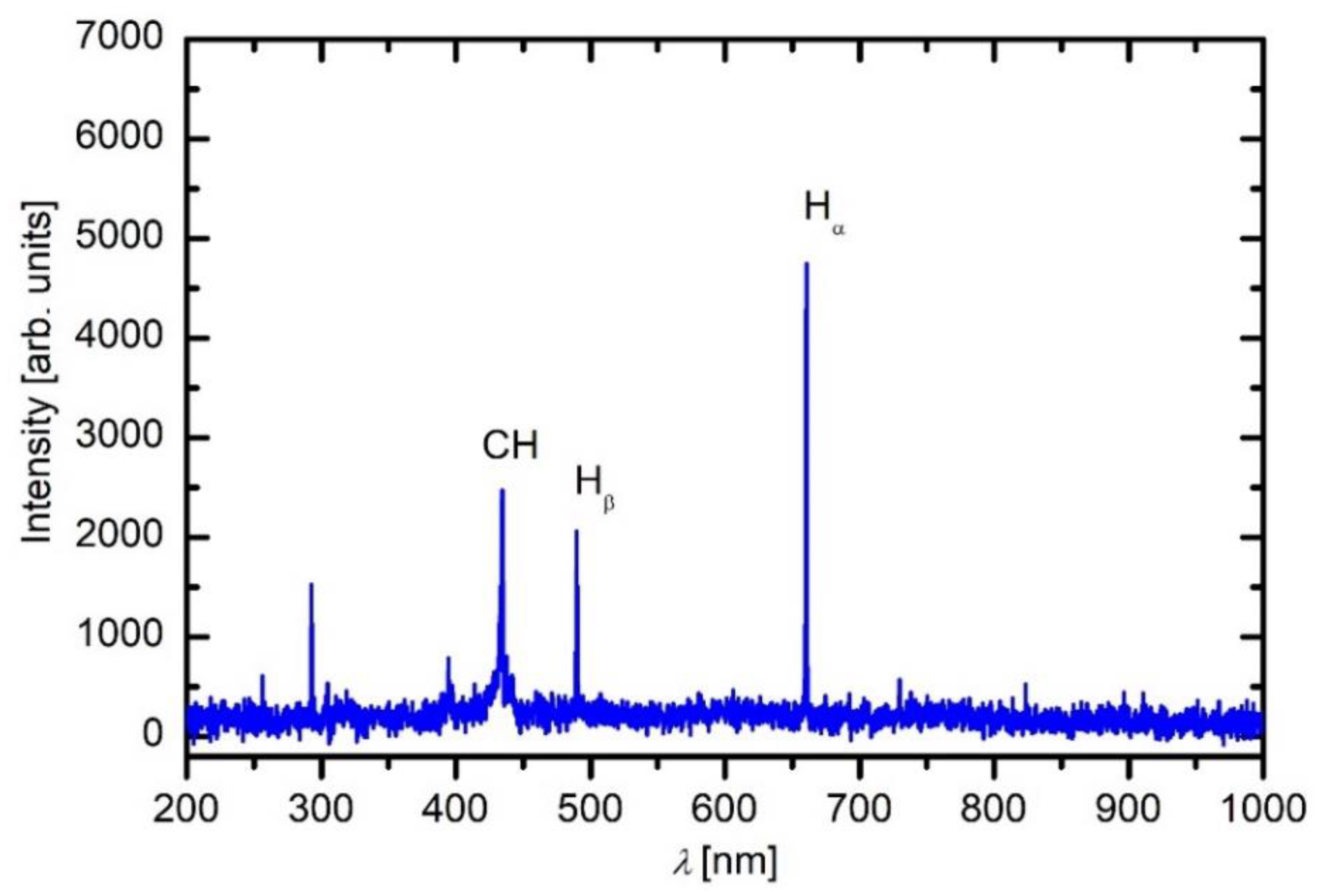
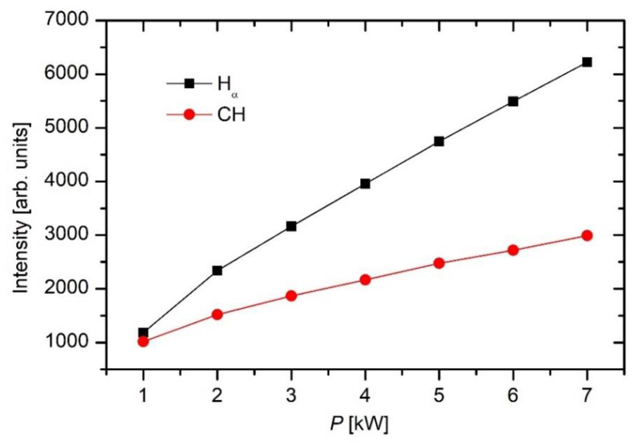
Plasma in the empty discharge chamber was characterized by OES. Here it should be stressed that an empty chamber means that there are no samples and no planetaria (sample holders) inside the reactor. A typical OES spectrum is shown in
Figure 3. The spectrum consists of Balmer series of radiative transitions of H atoms from excited states to the first excited state. The next prominent spectral feature arises from the relaxation of the CH radicals with the bandhead at 431 nm. Other features are marginal. The OES indicates partial dissociation of the precursor molecules, but otherwise, it does not provide any additional significant information. Other radicals are also in the reactor, but their emission is marginal. More interesting is the intensity of the spectral features versus the discharge power.
Figure 4 shows quite linear curves. The emission intensity depends on the electron density and temperature as well as the density of radicals in the ground state, and the dependence is not trivial. Still, the behavior of the lines in
Figure 4 indicates either more extensive dissociation of the precursor molecules or higher electron density/temperature or both at higher power. This observation is expected, considering that the optical lens for acquiring spectra was mounted just next to the powered electrode.
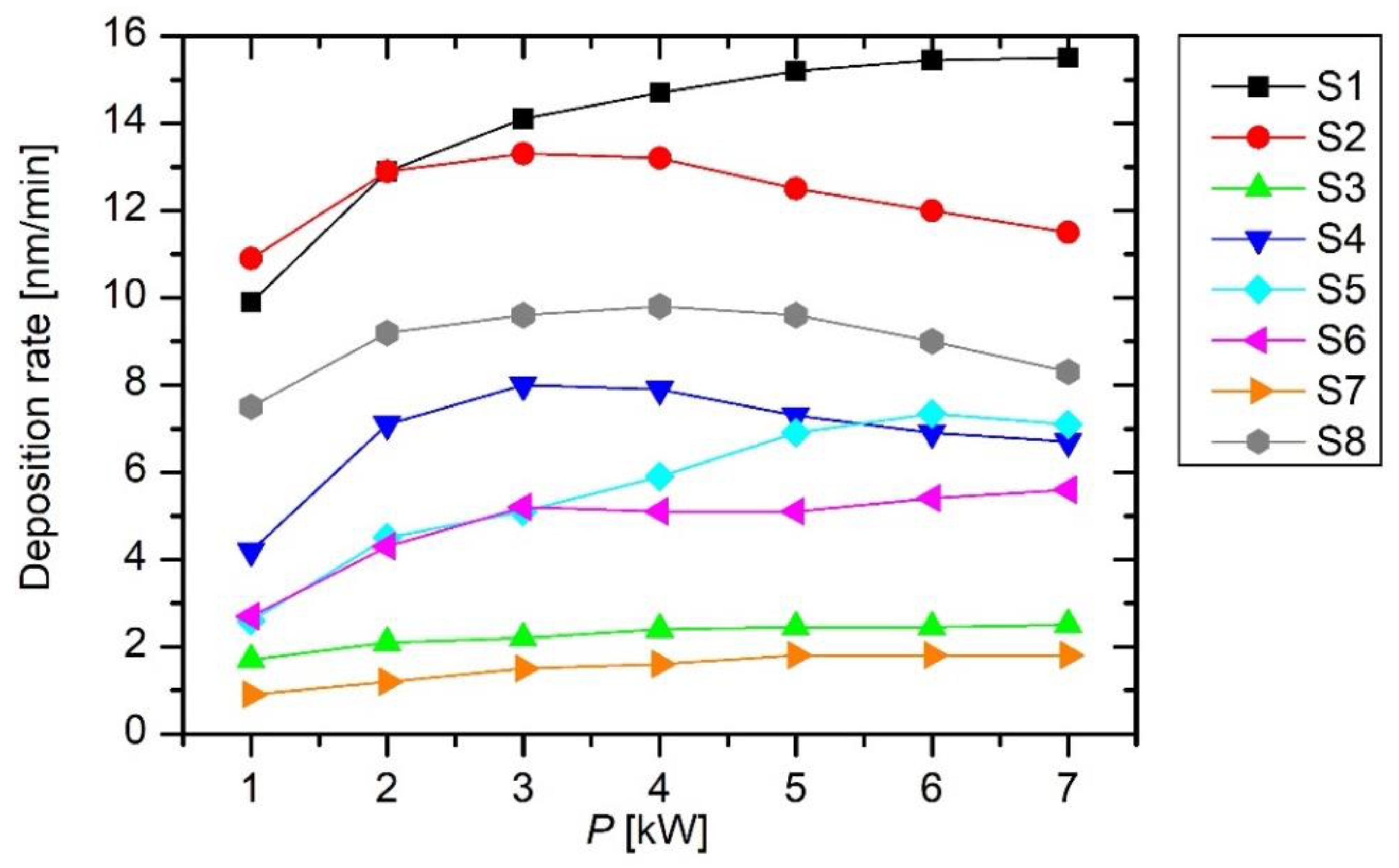
Figure 5 shows the measured deposition rate versus the discharge power. Interestingly enough, the deposition rate is rather constant in the broad range of powers from approximately 2 to 7 kW. This observation is not correlated with data in
Figure 4, which shows a gradual increase in the emission intensity. This paradox can be explained by a fact already reported for small experimental systems [
16]: only moderate dissociation of the precursor is sufficient for a reasonable deposition rate. Extensive dissociation of the precursor leads to the formation of various radicals that do not stick to the sample surface but are pumped out from the system; therefore, in cases where large power densities are used for sustaining plasma in HMDSO, the deposit does not resemble PDMS but rather silica. Detailed study of the transition from polymer-like films to films rich in silicon oxides was reported in [
16]. The power density used in this study was at least 10 times lower than the power density needed for such full transition; however, there are still mild transitions, towards films richer in silicon, that can affect the deposition rates seen in
Figure 5.
Figure 6 shows the thickness of the coating obtained from the sensors’ signals versus the treatment time for the empty plasma reactor. One can observe almost perfectly linear behavior, which indicates excellent stability of plasma parameters during the deposition of the protective coatings. The stability may be a consequence of the appropriately low pressure in the reactor, which prohibits instabilities that may appear because of the cluster formation [
27] and thus the loss of radicals useful for the deposition of the protective coating.
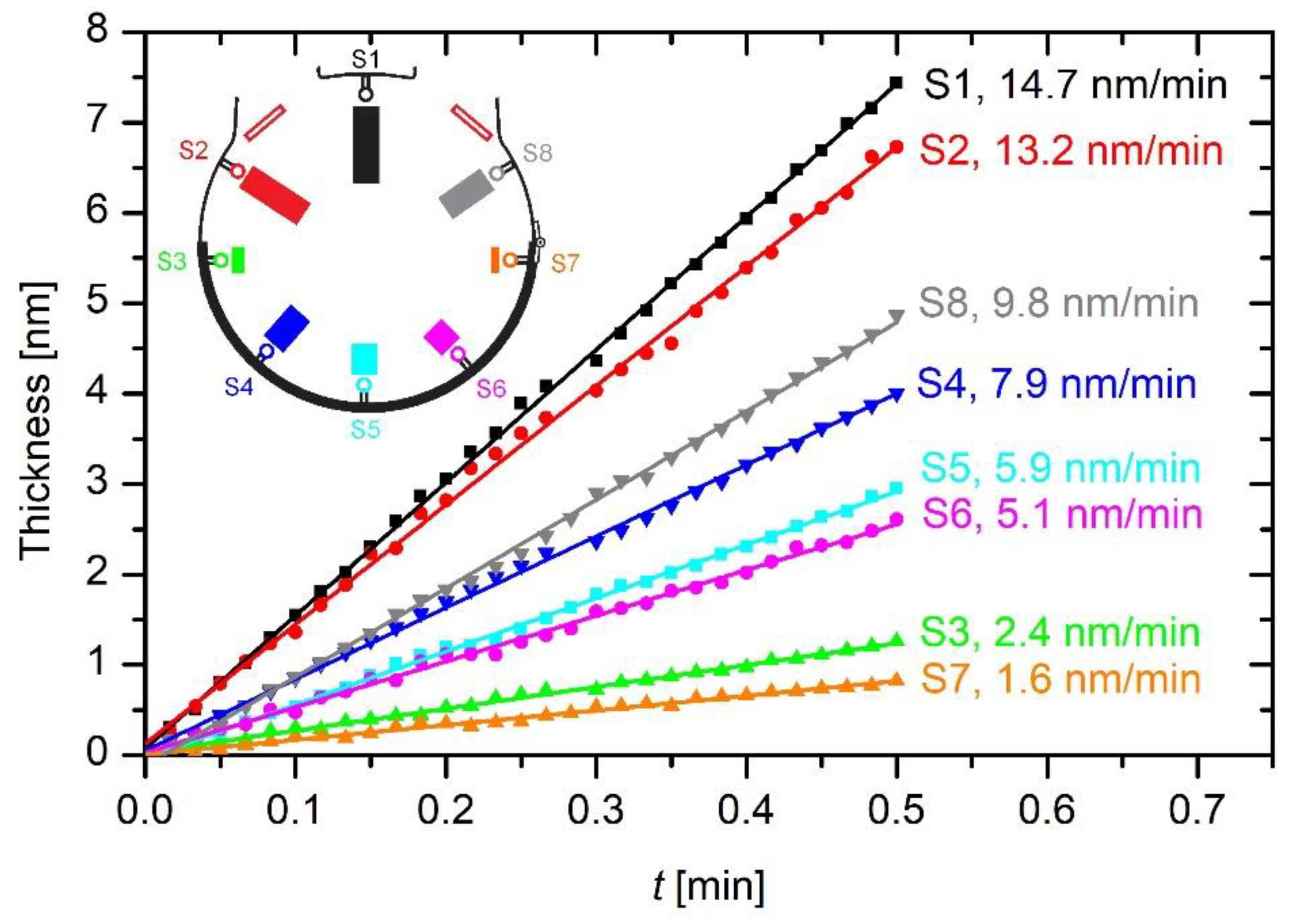
Both
Figure 5 and
Figure 6 indicate large differences in the deposition rate at different locations ranging from 1.6 to 14.7 nm min
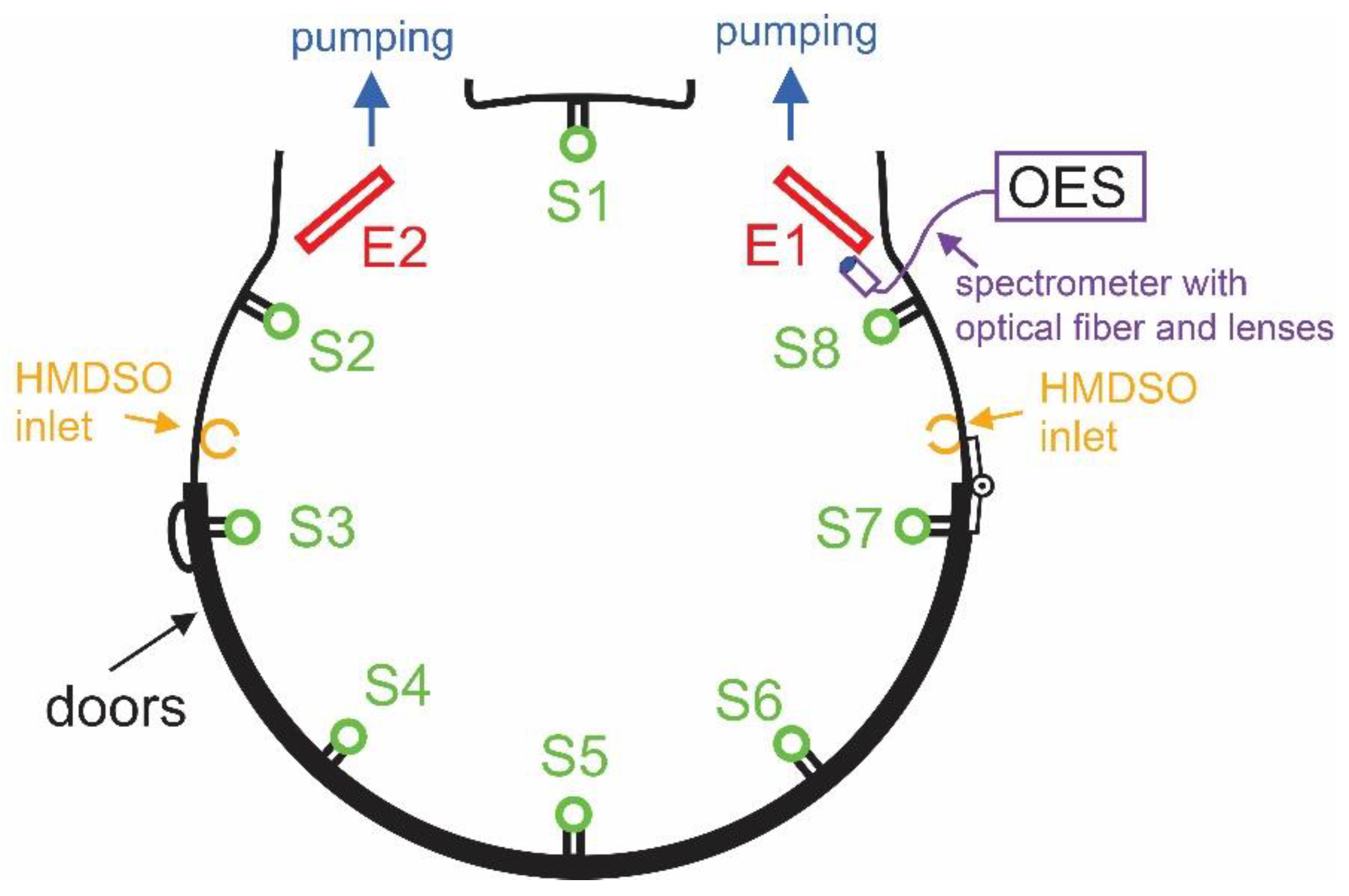
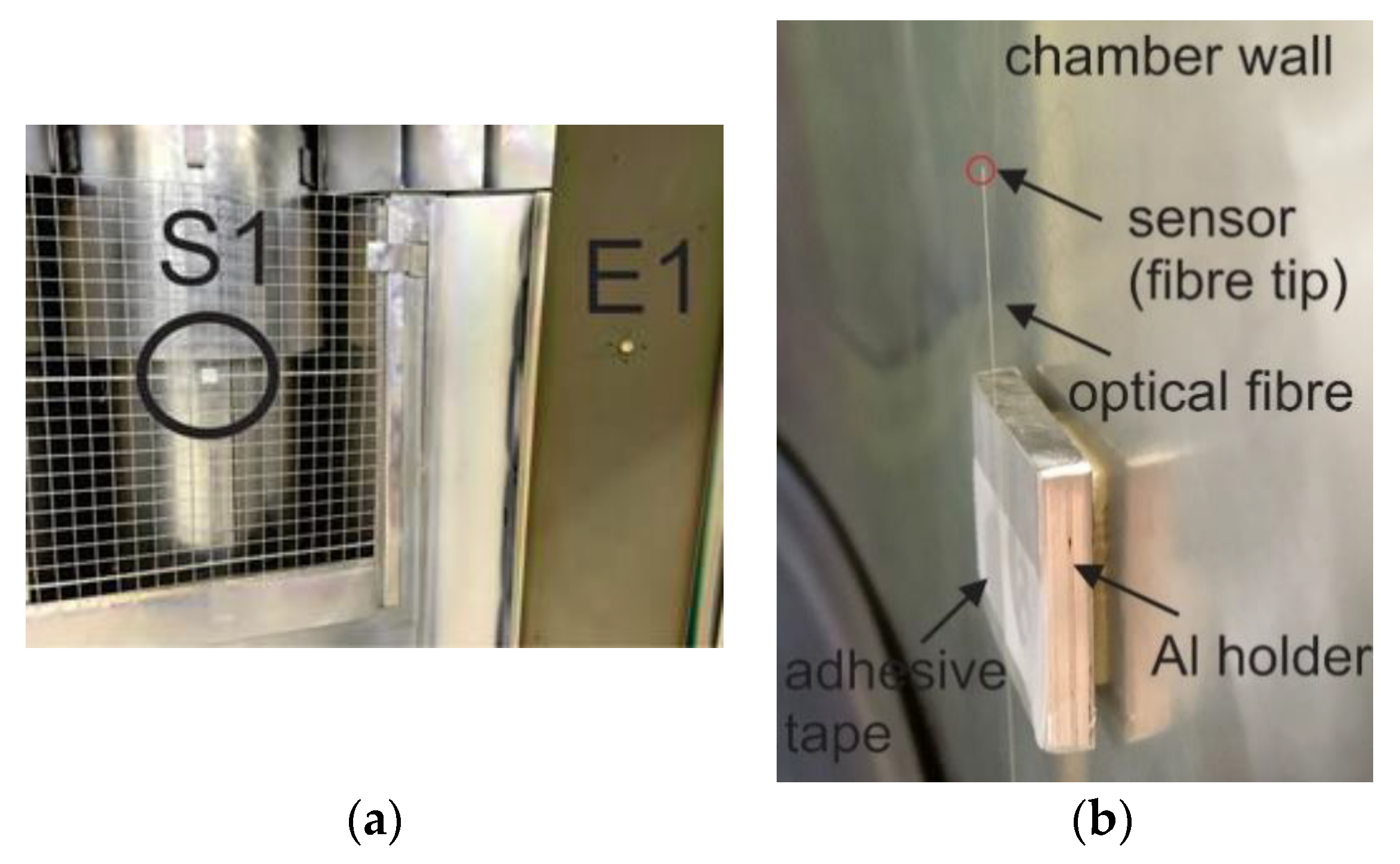
–1. The deposition rate is the largest for sensor S1. This sensor was placed on the grid between the electrodes, as shown in
Figure 1 and
Figure 2. The highest deposition rate is on the surface, where it is not needed because the radicals at the position of S1 are likely to be pumped away from the system. The high deposition rate indicates a high density of radicals that are capable of forming the protective coating. According to the state-of-the-art, such radicals are partially dissociated HMDSO molecules, including those found at the mass of 148 Da [
19]. In the empty chamber, these radicals are denser or more concentrated at the position near the pump ducts than anywhere else in the system, as revealed in
Figure 5 and
Figure 6.
Examining
Figure 5 and compared to
Figure 1, one observes the next largest deposition rate at sensors S2 and S8, which were located a bit farther from the pump ducts. In fact, sensors S2 and S8 were located between the gas inlet and the powered electrodes, as shown in
Figure 1. The possible reasons for favored deposition rate at these positions will be discussed later in this report.
The deposition rates at the position of sensors far from the electrodes are lower but still reasonably high. For example,
Figure 5 reveals the deposition rates of about 6 nm min
–1 for the sensors S4, S5, and S6. Conversely, sensors S3 and S7, which were placed close to the gas inlet but away from the powered electrodes, show a poor deposition of approximately 2 nm min
–1.
The distribution of the deposition rate in the plasma reactor provides a qualitative model of the gas kinetics that allows the most reasonable degree of fragmentation of the precursor molecules. The injected HMDSO molecules do not interact with the solid materials but should be partially dissociated to radicals with a reasonable sticking coefficient. The plasma density far from the powered electrodes in the reactor used for these experiments is only on the order of 10
14 m
–3 [
23]. Such a low density of electrons does not enable immediate dissociation to useful fragments. This may explain the poor deposition rates detected by sensors S3 and S7, located close to the gas inlet but away from the powered electrodes. The molecules should be allowed a prolonged residence time in the weakly ionized gaseous plasma to dissociate into useful radicals. The residence time will be estimated later in this paper. The injected precursor molecules enter the plasma reactor with a significant drift velocity but quickly thermalize (assume the random motion after a few elastic collisions). The motion is then governed by diffusion, i.e., it is random. The molecules suffer numerous collisions with plasma electrons while diffusing from the source (gas inlet) to the position of the sensors S4, S5, and S6. The gas at the position of these sensors is thus reasonably well dissociated, which favors the deposition on the surfaces far away from the electrodes. As mentioned above, the residence time of the injected molecules is too short to cause significant deposition at the positions of sensors S3 and S7.
Sensors S2 and S8 are as close to the gas inlet as S3 and S7, but
Figure 5 indicates a deposition rate several times higher at S2 and S8 compared to S3 or S7. This paradox may be explained by the larger residence time of molecules striking the surface of the sensors at positions S2 and S8, but the variation of the plasma density versus the distance from the powered electrode may be more important. The asymmetric capacitively coupled RF discharge is characterized by an oscillating sheath next to the powered electrode. Since the frequency of these oscillations is rather low (the RF generator operates at 40 kHz), the electrons oscillate within the sheath and gain energy enough for a rather extensive dissociation and ionization of the gaseous molecules within the oscillating sheath [
28]. Therefore, the dissociation of the precursor molecules is more extensive next to the electrodes than in the bulk plasma far away from the powered electrodes. As a result, the deposition rate at the sensors S2 and S8 is favorable despite the proximity of the gas inlet.
The radicals stick to surfaces of any material facing plasma; therefore, the deposition rate as determined by the sensors located in the reactor according to
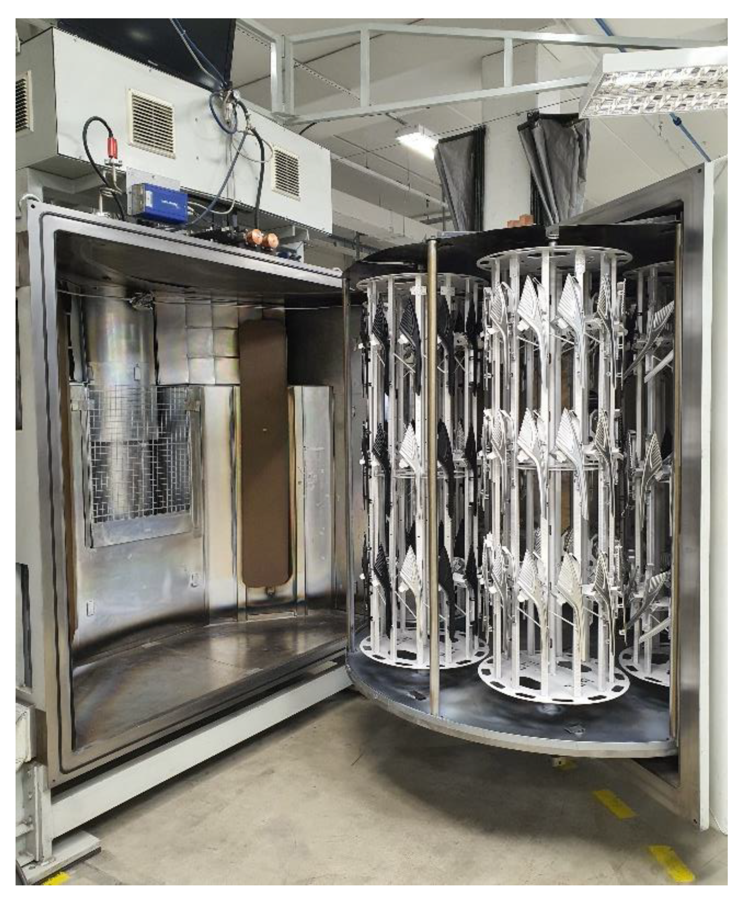
Figure 1 should be lower if the reactor is additionally loaded with samples. To study the influence of samples on the deposition rate, samples were mounted on the planetaria, as shown in
Figure 7. About 250 medium-sized, approximately 40-cm-long samples, which represented about 100% of the total chamber capacity, were evenly distributed inside the chamber. The height and the diameter of the planetaria were 160 cm and 55 cm, respectively, and the distance between axles was around 60 cm. The planetaria were spinning at a speed of 6 rpm. The deposition rate measurements were repeated with sensors located at the same positions as in the empty chamber. The results are shown in
Figure 8. The highest deposition rate was observed for the sensors S2 and S8. These sensors are located between the gas inlet and the powered electrode (
Figure 1). The deposition rate at the positions S2 and S8 are about an order of magnitude greater than at any other position except near the pump ducts. The presence of samples in the plasma reactor, therefore, influences the deposition rate significantly. Not only is it lower than in the empty reactor (compare
Figure 6 and
Figure 9), but a reasonably large deposition rate is observed only in the region close to the electrodes (S2, S8, and S1). Elsewhere, the deposition rate is below 1 nm min
−1.
The very low deposition rate at S4, S5, and S6, as observed in
Figure 8, is explained by the loss of radicals on the surfaces of the samples. As discussed above, the plasma density away from the electrodes is low, so the loss of radicals useful for depositing protective coating cannot be balanced by production because of electron-impact dissociation. Conversely, the deposition rate close to the powered electrode (sensors S2 and S8) remains reasonably high because of the higher electron energy in the oscillating sheath.
The ratio between the deposition rate in an empty reactor and a full reactor is shown in
Figure 9. The highest ratio of 10–20 is observed for sensors positioned far from the electrodes. This observation was already explained by the loss of radicals on the surface of the samples. However, the ratio is much lower for the sensors positioned close to the powered electrodes. For sensors S2 and S8, the ratio is approximately 3 for the lowest power of 1 kW and only 2 for the highest power of 7 kW. The power-dependence of the ratio is explained by the fact that the electron energy in the vicinity of the powered electrodes is much higher than far from the electrodes, so a significant fraction of injected HMDSO molecules get dissociated and thus contribute to the film growth.
The upper discussion reveals the crucial role of the residence time of molecules in the plasma reactor. Gaseous molecules diffuse in the plasma reactor because the random velocity is much higher than the drifting from the gas inlet to the pump ducts. The drift velocity of gaseous molecules at the entrance to the pump ducts can be calculated if the effective pumping speed at that position is known. The effective pumping speed depends on the nominal pumping speed of the roots pumps and the conductivity of any vacuum elements mounted between the roots pumps and the plasma reactor. The conductivity is difficult to determine, but one can also determine the effective pumping speed from the measured gas flow and pressure inside the reactor by considering the constant mass flow:
Here,
p1 is the atmospheric pressure,
S1 is the gas flow as measured by the flow controller,
p2 is the measured pressure in the plasma reactor, and
S2 is the effective pumping speed at the grid which separates the plasma reactor and the pump ducts. Taking into account the measured values, i.e.,
p1 = 10
5 Pa,
S1 = 130 cm
3/min = 2×10
−6 m
3 s
–1,
p2 = 4 Pa, one can estimate the effective pumping speed as:
As calculated from Equation (1), the effective pumping speed is an order of magnitude lower than the nominal pumping speed of the roots pumps. This observation may be explained by the deviation of the real pumping speed of the roots pumps from the nominal value (the latter is just the maximum pumping speed at optimal conditions) and the limited conductivity of vacuum elements mounted between the plasma reactor and the roots pumps.
There is a negligible pressure gradient throughout the plasma reactor, because the conductivity is orders of magnitude greater than the effective pumping speed. The cross-section of the plasma reactor is a product of the reactor diameter and height, i.e.,
A = 3.5 m
2. The gas drift velocity from the source to the pump ducts is:
This value is orders of magnitude lower than the random velocity due to the thermal motion of the molecules, which is:
In Equation (4), we considered the room temperature (
T = 300 K) and the HMDSO mass
m = 162 Da. By considering the distance between the gas inlet and the grid separating the reactor from the pump ducts of
l = 1 m, one can estimate the average residence time of gaseous molecules as:
The residence time as calculated from Equation (5) is an averaged value taking into consideration the simple calculations. Because the random velocity as calculated from Equation (4) is orders of magnitude higher than the drift velocity as determined from Equation (3), the residence time is spread broadly from the value calculated using Equation (5), and thus it should be taken just as an estimation. In any case, the residence time is long enough to assure for numerous collisions with plasma electrons. The large residence time is the reason for the rather large deposition rate at any position far from the gas inlet in the empty reactor. The maximal deposition is observed on the grid near the pump ducts (sensor S1) in the empty reactor. The radicals entering the pump ducts are likely to have been created well before reaching the grid.
Plasma reactors are useful only when the coatings are deposited on various products mounted on the planetaria. Technologically relevant results are presented in
Figure 8. The deposition rate at sensor S1 (mounted on the grid near the pump ducts) is moderate at about 2 nm min
–1, which is favorable from the technological point of view. Still, a significant fraction of the radicals useful for the thin film deposition is pumped out from the reactor. However, the major deficiency of the plasma reactor is the poor deposition rate at any other position. Despite the long residence time of gaseous radicals, the deposition rate is poor because of the loss of radicals on the samples placed on the planetaria. The only useful part of the reactor, when loaded with samples, is at positions S2 and S8, so close to the powered electrodes. The discharge configuration in this reactor is, therefore, inadequate. The configuration with electrodes placed opposite to the pump duct should be better.
No sensor was placed on a powered electrode because it would heat significantly. Still, according to the measured deposition rates and according to the above discussion, it is reasonable to assume the large deposition rate on the powered electrodes. In fact, the electrodes should occasionally be etched in chemical baths to remove the excessive deposits. The extensive deposition of thin films on the electrodes and thus loss of radicals for coating the samples is a major drawback of the reactor used in this study. The problem could be minimized using symmetric discharge, but it is often not feasible as in our PECVD reactor.
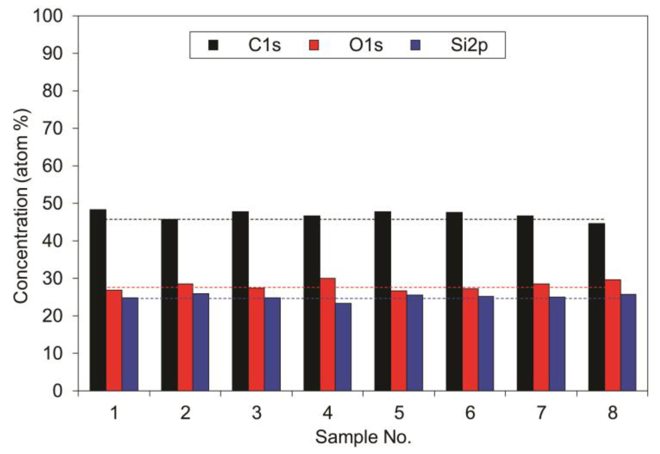
Despite the large dissipation of the deposition rate, the composition of the deposited films remains similar for all films at the positions of different sensors.
Figure 10 represents the composition of the films as deduced from XPS survey spectra. The measurements were performed in the reactor loaded with samples. The concentration of carbon is close to 50 at.%, while the concentrations of oxygen and silicon is between 25 and 30 at.% for all samples. The small variations in the composition may be attributed to the accuracy of the XPS technique or to actual variation in the composition, but because the differences are marginal it is possible to conclude that the stoichiometry of the deposited films does not vary significantly between different positions in the plasma reactor.


 ,
, 
