Article

Plasma Etching Behavior of SF6 Plasma Pre-Treatment Sputter-Deposited Yttrium Oxide Films

1
Department of Materials Science and Engineering, Da-Yeh University, Changhua 51591, Taiwan
2
Graduate Institute of Materials Science and Green Energy Engineering, National Formosa University, Huwei, Yunlin 632, Taiwan
3
Department of Industrial Engineering and Management, Da-Yeh University, Changhua 51591, Taiwan
*
Author to whom correspondence should be addressed.
Coatings 2020, 10(7), 637; https://doi.org/10.3390/coatings10070637
Submission received: 9 June 2020 / Revised: 25 June 2020 / Accepted: 28 June 2020 / Published: 30 June 2020
(This article belongs to the Section Corrosion, Wear and Erosion)

Abstract

:
Yttrium oxyfluoride (YOF) protective materials were fabricated on sputter-deposited yttrium oxide (Y2O3) by high-density (sulfur fluoride) SF6 plasma irradiation. The structures, compositions, and fluorocarbon-plasma etching behaviors of these films were systematically characterized by various techniques. After exposure to SF6 plasma, the Y2O3 film surface was fluorinated significantly to form a YOF film with an approximate average thickness of 30 nm. X-ray photoelectron spectroscopy revealed few changes in the elemental and chemical compositions of the surface layer after fluorination, confirming the chemical stability of the YOF/Y2O3 sample. Transmission electron microscopy confirmed a complete lattice pattern on the YOF/Y2O3 structure after fluorocarbon plasma exposure. These results indicate that the SF6 plasma-treated Y2O3 film is more erosion resistant than the commercial Y2O3 coating, and thus accumulates fewer contamination particles.

1. Introduction

In recent years, semiconducting integrated circuits (ICs) have progressed toward various functionalities on single electrical chips, and have been downscaled to nanometer size [1]. Reducing the influence of particle contaminants in silicon wafers is becoming increasingly critical because such particles decrease the mass-production yield of ICs [2,3]. In particular, the corrosive gases (e.g., C2F6, CF4, CHF3, and C4F6) used in semiconductor manufacturing processes generate high-density fluorocarbon plasma that bombards the IC chip and reacts with its inner chamber wall and ceramic parts (such as chamber windows, electrodes, showerhead cover baffles, and rings), generating contaminant particles [4,5,6]. Ceramics are desired as plasma-resistant materials on parts of plasma equipment, by virtue of their high hardness, high wear resistance, dielectric strength and chemical stability [7,8,9]. The plasma-facing inner wall of the chamber is often coated with yttrium oxide (Y2O3), which provides superior plasma erosion resistance on silicon-based materials, and also extends their lifetime. However, the reaction between Y2O3 and fluorine plasma generates thin fluorinated particles at the grain boundaries [10,11,12]. Recently, yttrium fluoride (YF3) coatings have been proposed as potential alternative ceramic materials for Y2O3 because they prevent the generation of fluoride particles. The standard enthalpy of the metal–oxygen bond is lower in YF3 (−392 kJ mol–1) than in Y2O3 (−318 kJ mol−1), indicating that YF3 is more chemically stable than Y2O3 [13,14,15]. Ceramic protective coatings on chamber walls are typically fabricated by plasma spray techniques. However, although the rapid deposition forms thick films, spray methods tend to produce porous structures and rough surfaces, resulting in critical particle impurities [16]. These problems in the semiconductor plasma-etching process are believed to be resolved by vacuum coating techniques, such as radio frequency (RF) magnetron sputtering, but when YF3 target is sputtered by these techniques, the stoichiometric variations in the Y/F ratio cause fluorine atom deficiencies from the target to the substrate, resulting in non-stoichiometric films with possibly degraded plasma erosion resistance [17,18]. Existing studies have focused on yttrium oxyfluoride (YOF) as a protective coating of the parts inside the manufacturing equipment chambers of semiconductor plasma processes [19,20]. In our previous study, we reported the formation of a YOF-altered thin layer on Y2O3 and YF3 coatings surfaces [21]. Furthermore, we also evaluated the characteristics of YOF coating fabricated by atmospheric plasma spraying. The YOF coating exhibited higher mechanical and electrical properties than those of the YF3 coating [22]. The end result was fewer contaminants in the semiconductor IC products [23]. In the present paper, we develop an SF6 plasma treatment that generates a YOF-altered layer on the Y2O3 surface and evaluate the etching behaviors of the Y2O3 and YOF/Y2O3 layers under fluorocarbon plasma exposure.

2. Materials and Methods

Y2O3 thin films were deposited on commercial c-plane sapphire substrate by RF magnetron sputtering (SSI-100, Shihsin, Tainan, Taiwan) in a vacuum chamber. Y2O3 ceramic target (99.99% purity, 2 inch diameter, 3 mm thickness) was prepared as a source for film deposition. Prior to film deposition, the substrates were sequentially cleaned in acetone and alcohol, and then by ultrasonic cleansing in de-ionized water for 30 min. The cleaned substrates were blow-dried in nitrogen gas. The sputtering gas was high-purity argon (99.995%) maintained at a constant flow rate (~100 sccm). The sputtering process was performed in a base chamber pressure of approximately 1.5 × 10⁻⁵ Torr, preserved with turbo molecular and oil diffusion pumps. Plasma generation was activated by RF power at 13.56 MHz. The target–substrate distance was 15 cm. To ensure a uniform film thickness, the substrate holder was rotated at 20 rpm during the deposition process. The substrate heating temperature was varied from 200 to 600 °C in steps of 200 °C. After the Y2O3 thin-film deposition, the specimens were exposed to reactive ion etching (RIE). The plasma treatment time was 300 s, the process gas was SF6 (30 sccm under a pressure of 100 Torr), and a RIE power (bias) of 100 W. The plasma etching of all samples was performed in an inductively-coupled plasma etcher (ICP, EIS-700, Elionix, Tokyo, Japan). The etching gases were mixed CF4 and O2 (25 sccm CF4 and 5 sccm O2). The crystallographic properties of Y2O3 films were investigated via an X-ray diffractometer (XRD, XRD-6000, Shimadzu, Kyoto, Japan) with Cu Kα X-ray source (λ = 1.541874 Å) radiation. The crystallite size and full width at half maximum (FWHM) of the Y2O3 film grown on the sapphire substrate were calculated using the Debye–Scherer equation. The surface morphologies, microstructures and compositions of the as-deposited Y2O3 and SF6 plasma-treated Y2O3 films were analyzed by field emission scanning electron microscopy (FE-SEM, S-3000H, Hitachi, Tokyo, Japan), atomic force microscopy (AFM, DI-3100, Veeco, New York, NY, USA), high-resolution transmission electron microcopy (HRTEM, H-600, Hitachi, Tokyo, Japan) and X-ray photoelectron spectroscopy (XPS, PHI 5000 VersaProbe, ULVAC-PHI, Kanagawa, Japan) using a monochromatic Cu Kα X-ray source (λ = 1.541874 Å) at a passing energy of 20 eV with a spot size of 650 μm.

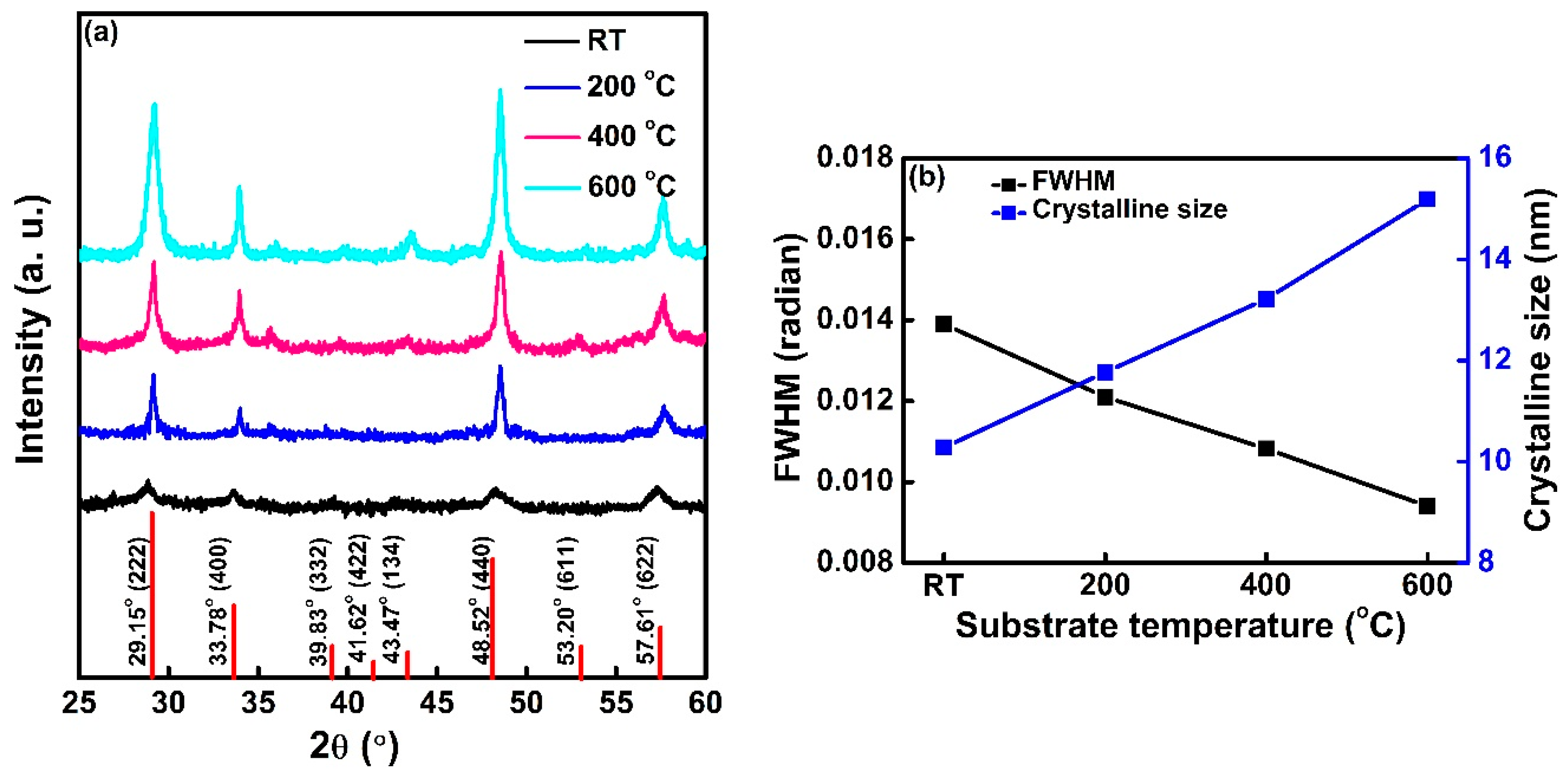
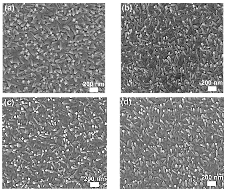
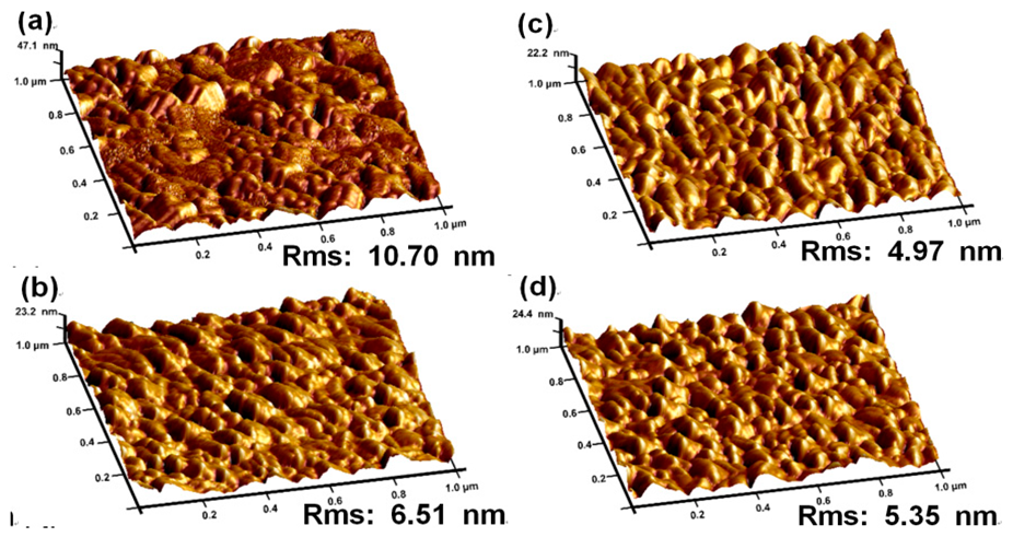
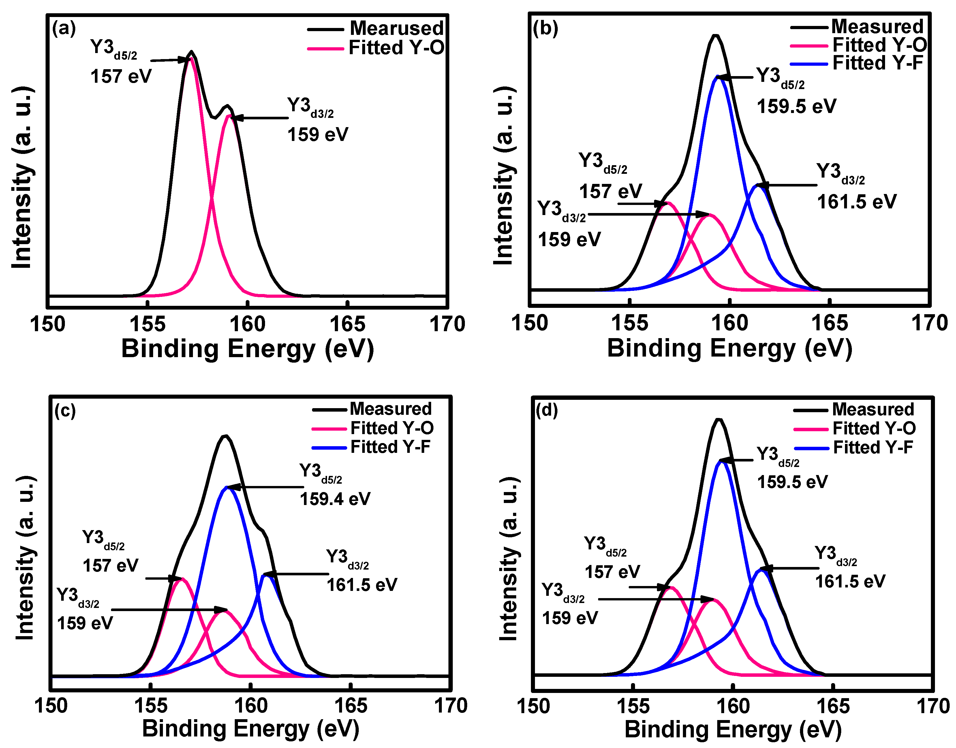
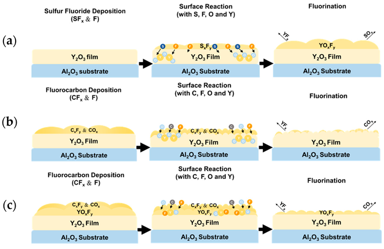
3. Results and Discussion

Figure 1a shows the XRD patterns of the Y2O3 films deposited at different substrate temperatures. The polycrystalline nature of all deposited Y2O3 films was indexed to JCPDS card file 43-1036. Four clear diffraction peaks of Y2O3 (222), (400), (440) and (622) appeared on the substrate deposited at 600°C. Those of the Y2O3 (222) peak deposited at different substrate temperatures are shown in Figure 1b. Increasing the substrate temperature from 200 to 600 °C increased the crystalline size from 10.5 to 15.2 nm and narrowed the FWHM of the (222) peak. The higher substrate temperature supplied sufficient energy to enhance the mobility of the atoms and to further improve the film crystallites. Subsequent analyses were performed on the sample prepared at 600 °C, which showed a dense structure in the XRD analysis result.
Figure 2 shows the FE-SEM images of the as-deposited Y2O3 and SF6 plasma-treated Y2O3 film surface before and after fluorocarbon plasma etching. The plasma etching decreased the flake polygon size of the as-deposited Y2O3 films (Figure 2b), but did not significantly alter the film surface morphology (Figure 2c). This indicates that the SF6 plasma-treated Y2O3 was robust to irradiation with fluorocarbon plasma. The chemical stability of the SF6 plasma-treated Y2O3 might be attributable to the thin YOF layer formed on the Y2O3 surface (YOF/Y2O3). Figure 3 shows the surface morphologies of the as-deposited Y2O3 and SF6 plasma-treated Y2O3 films before and after fluorocarbon plasma etching, obtained by AFM. After fluorocarbon plasma etching, the root mean square (RMS) roughness values of the as-deposited Y2O3 films decreased from 10.7 to 4.97 nm, but those of the plasma-treated Y2O3 sample decreased only from 6.51 to 5.35 nm. The small RMS difference in the latter sample might be attributed to the YOF-altered layer formed on the plasma-treated Y2O3 surface. The Y–F bonds formed by YOF in the film might reduce the reactivity of YOF with fluorine radicals during the etching process [24].
The effects of the as-deposited Y2O3 films and SF6 plasma-treated Y2O3 films before and after fluorocarbon plasma etching were determined by XPS. The wide energy spectra of the films are shown in Figure 4. To generate the atomic signals for the XPS measurements, the samples were bombarded by an argon beam for 60 s. The XPS peaks in the as-deposited Y2O3 film contained Y and O elements. After exposure to SF6 plasma, an intense F1s peak appeared in the spectrum of the Y2O3 film. This peak can be attributed to the penetration of fluorine radicals into the film. The fluorine radicals partially substituted the oxygen atoms, forming a fluorine-rich layer on the surface. By contrast, the XPS spectrum of the SF6 plasma-treated sample was unaffected by fluorine-plasma etching. The quantitative XPS evaluations of F (fluorine), Y (yttrium), and O (oxygen) are listed in Table 1. Exposure to fluorocarbon plasma marginally altered the chemical composition of the SF6 plasma-treated Y2O3 film but largely changed the O 1S and F 1S contents of the as-grown Y2O3 film. Similar results were reported in a previous study of fluorocarbon plasma etching [25].
Figure 5 shows the XPS spectra of yttrium atoms in the as-deposited Y2O3 films and SF6 plasma-treated Y2O3 films before and after fluorocarbon plasma etching. In the curve-fitted XPS spectra of the Y2O3 films, the Y3d peak was divisible into two peaks representing cations with Y3d5/2 and Y3d3/2 electrons. The intensity ratio of these peaks and the binding energy difference between the peaks were ~3:2 and ~2.0 eV, respectively, consistent with the XPS analysis reported in the literature [26]. Before the as-deposited Y2O3 films reacted with the fluorine plasma, the binding energies of Y3d5/2 and Y3d3/2 peaked at 157 and 159 eV, respectively (see Figure 5a). In the spectrum of the Y2O3 films subjected to fluorine-plasma treatment, Y3d5/2 and Y3d3/2 deconvoluted into four binding energy peaks (Figure 5b). The two peaks at the low-binding energies (157 and 159 eV) correspond to Y–O bonding, whereas those at the higher binding energies (159.5 and 161.5 eV) are ascribed to Y–F bonding in the Y2O3 films. The Y–F bonds form because fluorine atoms have a higher electronegativity than oxygen atoms (4.0 vs. 3.5). Higher electronegativity promotes electron transfer to fluorine, decreasing the electron density around the cation and hence increasing the binding energy [27,28]. In the SF6 plasma-treated Y2O3 films, the locations of the XPS peaks were less changed after exposure to fluorocarbon plasma (Figure 5c,d). This result agrees with a previous study on the fluorination mechanism of the YOF layer reaction with fluorine plasma [29].
Figure 6a shows a cross-sectional TEM image of the as-deposited Y2O3 films after surface irradiation by SF6 plasma. The fluorine-concentrated altered layer was approximately 20–40 nm thick, and contained multiple phases of YOF (104) and (006). The significantly increased altered layer on the Y2O3 surface is attributable to the large number of oxygen atoms in Y2O3 and the many vacancy reactions with SF6 plasma, which has a higher fluorine density than CF4/O2 plasma [30]. Figure 6b,c shows the as-deposited Y2O3 and the SF6 plasma-treated Y2O3 films after fluorocarbon plasma etching, respectively. After irradiation with fluorocarbon plasma, thin fluorinated altered layers were formed on the as-deposited Y2O3. This uneven fluorination layer with a disordered Moiré pattern and incomplete lattice fringes was observed near the Y2O3 surface. Surface damaged was caused by chemical reactions with the fluorine plasma. The damage layer was probably responsible for the cracks and particle contamination observed in Figure 6b [31]. Meanwhile, the surface of the SF6 plasma-treated Y2O3 exhibited no fluorinated layer, because the reaction with fluorocarbon plasma was prevented by the Y–F bonds and the high concentration of fluorine in the original film (Figure 6c).
Consistent with the XPS results, the plasma-treated Y2O3 films demonstrated no apparent chemical change after plasma irradiation. Therefore, the chemical erosion was slower on the SF6 plasma-treated Y2O3 films than on the as-deposited Y2O3 film. Based on these observations, we proposed a mechanism explaining the fluorine-plasma etching behavior on the as-deposited Y2O3 films and SF6 plasma-treated Y2O3 films (see Figure 7). The YOF on the Y2O3 surface forms by decomposition of the Y–O bonds under sulfur fluoride plasma. Owing to the smaller bonding energy of S–O than of Y–O (549 kJ/mol versus 685 kJ/mol), the S–O bond reacts more efficiently with the sulfur fluoride deposited film than the Y–O bond. The SF6 plasma-treated Y2O3 film etched by CF4/O2 plasma exhibited no notable chemical corrosion reactions. Therefore, the YOF/Y2O3 layer effectively reduces particle generation from erosion caused by fluorocarbon plasma.

4. Conclusions

We compared the etching behaviors of sputter-deposited Y2O3 films and SF6 plasma-treated Y2O3 films after exposure to CF4/O2 plasma. Cross-sectional TEM observations revealed a thick YOF-altered layer on the Y2O3 surface after SF6 plasma irradiation. The surface roughness change on the as-deposited Y2O3 was probably attributable to the disordered layer after exposure to fluorocarbon plasma. As evidenced in the XPS results, fluorocarbon plasma induced fewer chemical reactions on the SF6 plasma-treated Y2O3 surface than on the as-prepared Y2O3 films. The YOF film is expected to provide an excellent protective barrier against damage caused by the fluorine-plasma etching process.

Author Contributions

Conceptualization, W.-K.W.; data curation, S.-Y.W., Y.-J.X., K.-F.L., P.-C.T., Y.-H.Z., and S.-Y.H.; writing—original draft preparation, S.-Y.W., K.-F.L., S.-Y.H., and W.-K.W.; writing—review and editing, W.-K.W. All authors have read and agreed to the published version of the manuscript.

Funding

This research was funded by the Ministry of Science and Technology of Taiwan (Nos. 108-2221-E-212-007 and 109-2622-E-212-001-CC3).

Acknowledgments

The authors wish to express their sincere gratitude for the technical support from the advanced Industry Technology Centre of National Chung Hsing University, Taiwan.

Conflicts of Interest

The authors declare no conflict of interest.

References

  1. Ito, N.; Moriya, T.; Uesugi, F.; Matsumoto, M.; Liu, S.; Kitayama, Y. Reduction of particle contamination in plasma-etching equipment by dehydration of chamber wall. Jpn. J. Appl. Phys. 2008, 47, 3630–3634. [Google Scholar] [CrossRef]
  2. Yoo, S.W.; Hwang, N.M.; You, S.J.; Kim, J.H.; Seong, D.J. Control of nanoparticle size and amount by using the mesh grid and applying DC-bias to the substrate in silane ICP-CVD process. J. Nanopart. Res. 2017, 19, 374. [Google Scholar] [CrossRef]
  3. Cardinaud, C.; Peignon, M.C.; Tessier, P.Y. Plasma etching: Principles, mechanisms, application to micro- and nano-technologies. Appl. Surf. Sci. 2000, 164, 72–83. [Google Scholar] [CrossRef]
  4. Kasashima, Y.; Natsuko, N.; Uesugi, F. Instantaneous generation of many flaked particles by impulsive force of electric field stress acting on inner wall of mass-production plasma etching equipment. Jpn. J. Appl. Phys. 2013, 52, 066201. [Google Scholar] [CrossRef]
  5. Kim, D.M.; Jang, M.R.; Oh, Y.S.; Kim, S.; Lee, S.M.; Lee, S.H. Relative sputtering rates of oxides and fluorides of aluminum and yttrium. Surf. Coat. Technol. 2017, 309, 694–697. [Google Scholar] [CrossRef]
  6. Ma, T.; List, T.; Donnelly, V.M. Comparisons of NF3 plasma-cleaned Y2O3, YOF, and YF3 chamber coatings during silicon etching in Cl2 plasmas. J. Vac. Sci. Technol. A 2018, 36, 031305. [Google Scholar] [CrossRef]
  7. Song, J.B.; Kim, J.T.; Oh, S.G.; Shin, J.S.; Chun, J.R.; Yun, J.Y. Effect of sealing time of anodic aluminum oxide (AAO) film for preventing plasma damage. Sci. Adv. Mater. 2015, 7, 127–132. [Google Scholar] [CrossRef]
  8. Fukumoto, H.; Fujikake, I.; Takao, Y.; Eriguchi, K.; Ono, K. Plasma chemical behavior of reactants and reaction products during inductively coupled CF4 plasma etching of SiO2. Plasma Sources Sci. Technol. 2009, 18, 045027. [Google Scholar] [CrossRef]
  9. Duc, L.M.; Tan, C.M.; Luo, M.; Leng, I.C.H. Maintenance scheduling of plasma etching chamber in wafer fabrication for high-yield etching process. IEEE Trans. Semicond. Manuf. 2014, 27, 204–211. [Google Scholar] [CrossRef]
  10. Ashizawa, H.; Yoshida, K. Effect of the microstructures of yttrium ceramics on their plasma corrosion behavior. Ceram. Int. 2019, 45, 21162–21167. [Google Scholar] [CrossRef]
  11. Kim, C.S.; Kim, M.K.; Cho, H.; Park, T.E.; Yun, Y.H. Fabrication and plasma resistance of Y2O3 ceramics. Ceram. Int. 2015, 41, 12757–12762. [Google Scholar] [CrossRef]
  12. Kitamura, J.; Ibe, H.; Yuasa, F.; Mizuno, H. Plasma sprayed coatings of high-purity ceramics for semiconductor and flat-panel-display production equipment. J. Therm. Spray Technol. 2008, 17, 878–886. [Google Scholar] [CrossRef]
  13. Kim, D.M.; Oh, Y.S.; Kim, S.; Kim, H.T.; Lim, D.S.; Lee, S.M. The erosion behaviors of Y2O3 and YF3 coatings under fluorocarbon plasma. Thin Solid Film. 2011, 519, 6698–6702. [Google Scholar] [CrossRef]
  14. Akatsu, R.; Tsunoura, T.; Yoshida, K.; Yano, T.; Kishi, Y. Densification behavior of yttrium oxyfluoride ceramics by rate controlled sintering and their mechanical properties. Jpn. J. Appl. Phys. 2019, 58, SEEG02. [Google Scholar] [CrossRef]
  15. Kim, Y.; Kwon, H.; Prak, H.; Lee, C. Correlation of plasma erosion resistance and the microstructure of YF3 coatings prepared by vacuum kinetic spray. J. Therm. Spray Technol. 2020, 29, 1016–1026. [Google Scholar] [CrossRef]
  16. Kwon, H.; Kim, Y.; Park, H.; Lee, C. The importance of intimate inter-crystallite bonding for the plasma erosion resistance of vacuum kinetic sprayed Y2O3 coating. Surf. Coat. Technol. 2019, 374, 493–499. [Google Scholar] [CrossRef]
  17. Lei, P.; Zhu, J.Q.; Zhu, Y.K.; Han, J.C. Preparation and optical properties of sputtered-deposition yttrium fluoride film. Nucl. Instrum. Methods Phys. Res. Sect. B 2013, 307, 429–433. [Google Scholar]
  18. Su, W.T.; Li, B.; Liu, D.Q.; Zhang, F.S. The determination of infrared optical constants of rare earth fluorides by classical Lorentz oscillator model. J. Phys. D Appl. Phys. 2007, 40, 3343–3347. [Google Scholar] [CrossRef]
  19. Tsunoura, T.; Yoshida, K.; Yano, T.; Kishi, Y. Fabrication, characterization, and fluorine-plasma exposure behavior of dense yttrium oxyfluoride ceramics. Jpn. J. Appl. Phys. 2017, 56, 06HC02. [Google Scholar] [CrossRef] [Green Version]
  20. Shiba, Y.; Teramoto, A.; Goto, T.; Kishi, Y.; Shirai, Y.; Sugawa, S. Stable yttrium oxyfluoride used in plasma process chamber. J. Vac. Sci. Technol. A 2017, 35, 021405. [Google Scholar] [CrossRef]
  21. Lin, T.K.; Wang, W.K.; Huang, S.Y.; Tasi, C.T.; Wuu, D.S. Comparison of erosion behavior and particle contamination in mass-production CF4/O2 plasma chambers using Y2O3 and YF3 protective coatings. Nanomaterials 2017, 7, 183. [Google Scholar] [CrossRef] [PubMed] [Green Version]
  22. Lin, T.K.; Wuu, D.S.; Huang, S.Y.; Wang, W.K. Characteristics of yttrium fluoride and yttrium oxide coatings for plasma process equipment prepared by atmospheric plasma spraying. Jpn. J. App. Phys. 2016, 55, 126201. [Google Scholar] [CrossRef]
  23. Lin, T.K.; Wuu, D.S.; Huang, S.Y.; Wang, W.K. Preparation and characterization of sprayed-yttrium oxyfluoride corrosion protective coating for plasma process chambers. Coatings 2018, 8, 373. [Google Scholar] [CrossRef] [Green Version]
  24. Song, J.B.; Kim, J.T.; Oh, S.G.; Yun, J.Y. Contamination particles and plasma etching behavior of atmospheric plasma sprayed Y2O3 and YF3 coatings under NF3 plasma. Coatings 2019, 9, 102. [Google Scholar] [CrossRef] [Green Version]
  25. Wang, W.K.; Lin, X.Y.; Xu, Y.J. Structural and fluorine plasma etching behavior of sputter-deposition yttrium fluoride film. Nanomaterials 2018, 8, 936. [Google Scholar] [CrossRef] [Green Version]
  26. Hong, H.X.; Hong, J.M.; Cao, X.F.; Chen, X.; Xue, T. Ionic-liquid-assisted synthesis of YF3 with different crystalline phases and morphologies. Mater. Res. Bull. 2009, 44, 623–628. [Google Scholar]
  27. Kim, D.M.; Lee, S.H.; Alexander, W.B.; Kim, K.B.; Oh, Y.S.; Lee, S.M. X-ray photoelectron spectroscopy study on the interaction of yttrium-aluminum oxide with fluorine-based plasma. J. Am. Ceram. Soc. 2011, 94, 3455–3459. [Google Scholar] [CrossRef]
  28. Xia, J.J.; Liang, W.P.; Maio, Q.; Depla, D. The effect of energy and momentum transfer during magnetron sputter deposition of yttrium oxide thin films. Appl. Surf. Sci. 2018, 439, 545–551. [Google Scholar] [CrossRef]
  29. Tahara, R.; Tsunoura, T.; Yoshida, K.; Yano, T.; Kishi, Y. Fabrication of dense yttrium oxyfluoride ceramics by hot pressing and their mechanical, thermal, and electrical properties. Jpn. J. Appl. Phys. 2018, 57, 06JF04. [Google Scholar] [CrossRef]
  30. Miwa, K.; Takada, N. Fluorination mechanisms of Al2O3 and Y2O3 surfaces irradiated by high-density CF4/O2 and SF6/O2 plasmas. J. Vac. Sci. Technol. A 2009, 27, 831–839. [Google Scholar] [CrossRef]
  31. Miyashita, K.; Tsunoura, T.; Yoshida, K.; Yano, T.; Kishi, Y. Fluorine and oxygen plasma exposure behavior of yttrium oxyfluoride ceramics. Jpn. J. Appl. Phys. 2019, 58, EEC01. [Google Scholar] [CrossRef]
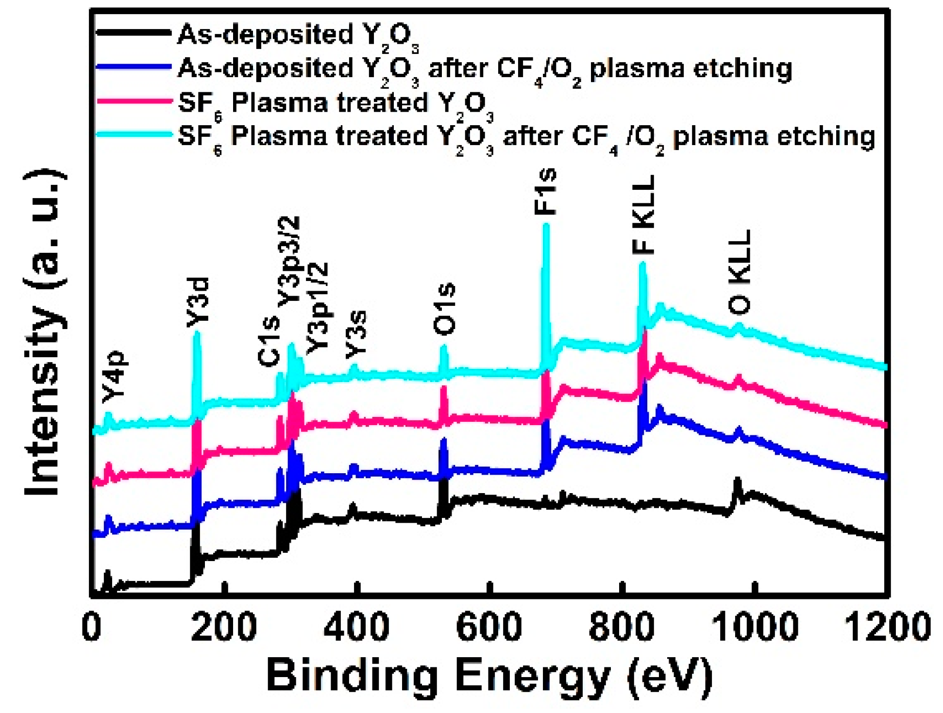
Figure 1. (a) XRD scans of the Y2O3 films grown at different substrate temperatures and (b) effect of substrate temperature on the average crystallite size and full width at half maximum (FWHM).
Coatings 10 00637 g001
Figure 2. Surface FE-SEM pictures of (a) and (b) the as-deposited Y2O3 films before and after fluorocarbon plasma etching, respectively, and (c) and (d) the SF6 plasma-treated films before and after fluorocarbon plasma etching, respectively.
Coatings 10 00637 g002
Figure 3. Atomic force microscopy (AFM) images of (a) and (b), the as-deposited Y2O3 films before and after fluorocarbon plasma etching, respectively, and (c) and (d), the SF6 plasma-treated films before and after fluorocarbon plasma etching, respectively.
Coatings 10 00637 g003
Figure 4. XPS survey spectra of the as-deposited Y2O3 films and SF6 plasma-treated Y2O3 before and after CF4/O2 plasma exposure.
Coatings 10 00637 g004
Figure 5. X-ray photoelectron spectra of (a) and (b), the as-deposited Y2O3 films before and after fluorocarbon plasma etching, respectively, and (c) and (d), the SF6 plasma-treated films before and after fluorocarbon plasma etching, respectively.
Coatings 10 00637 g005
Figure 6. Cross-sectional TEM images of the plasma-treated Y2O3 (a), and the as-deposited Y2O3 and SF6 plasma-treated Y2O3 before (b) and after (c) CF4/O2 plasma exposure. Right panels are magnified images of the areas enclosed by the blue squares in the left panels.
Coatings 10 00637 g006
Figure 7. Schematic of the SF6 plasma-treated films, and suggested mechanism of the CF4/O2 plasma-etching behavior on the as-deposited Y2O3 and SF6 plasma-treated films. (a) SF6 plasma-treated Y2O3; (b) as-deposited Y2O3 after CF4/O2 etching; (c) SF6 plasma-treated Y2O3 after CF4/O2 etching.
Coatings 10 00637 g007
Table 1. X-ray photoelectron spectroscopy (XPS) results of the as-deposited Y2O3 and SF6 plasma-treated Y2O3 film before and after exposure to CF4/O2 plasma.
TypeElemental Composition (at%)Atomic Ratio
Y3dF 1sO 1sC 1sF/Y
As-deposited28.383.3354.2214.070.12
CF4/O2 plasma etching21.8255.0916.057.042.58
SF6 plasma-treated24.8240.2725.529.391.62
CF4/O2 plasma etching23.2054.7517.584.472.36

