Recent Advances in Paper-Based Electronics: Emphasis on Field-Effect Transistors and Sensors

 ,
,  ,
, 

Abstract
1. Introduction
- Analyzing the integration of PFETs in modern paper-based systems;
- Categorizing PFETs by application domain (e.g., biosensing, logic gates, physical sensing);
- Evaluating detection techniques and critical performance metrics.
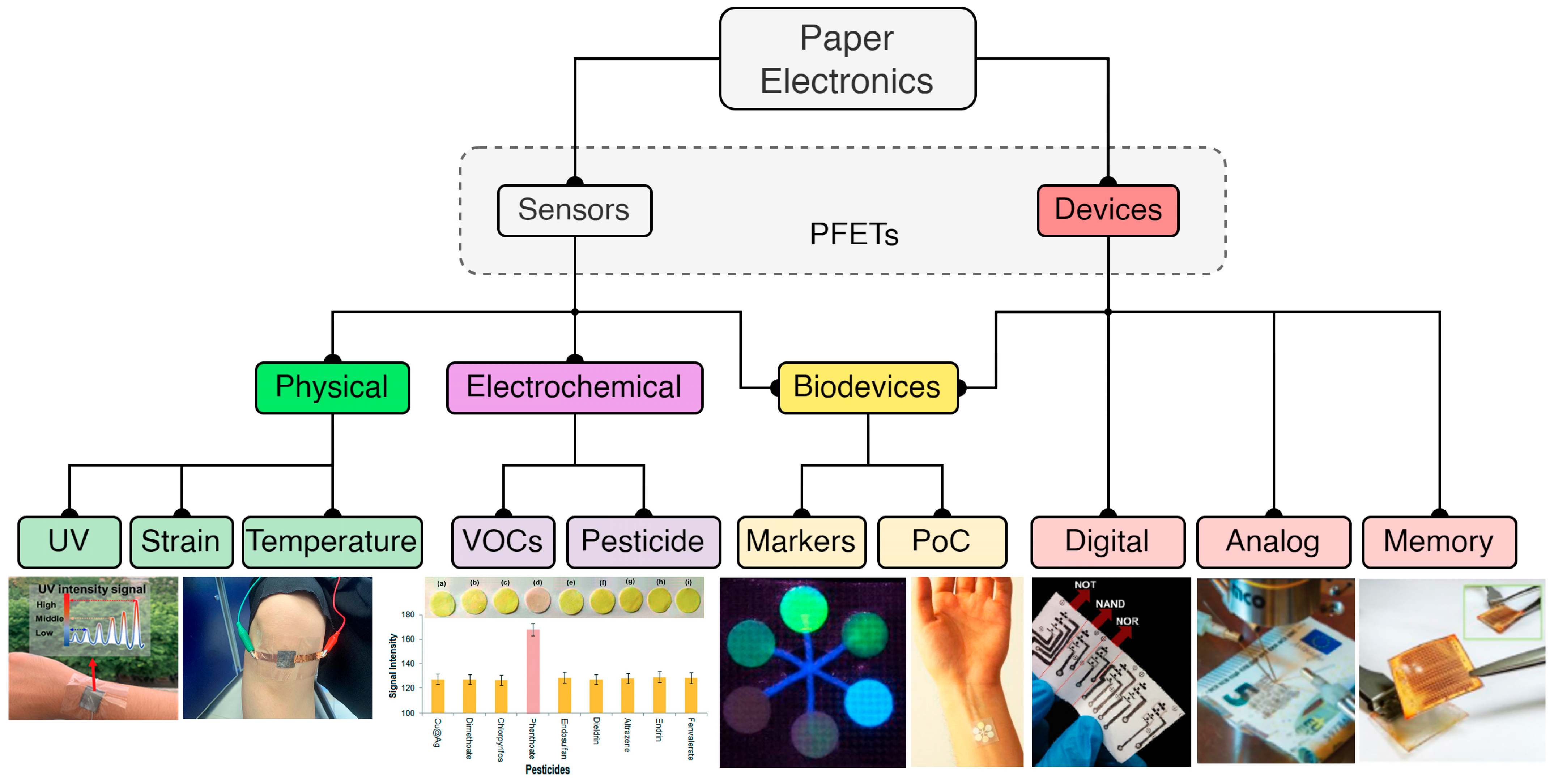
2. Paper-Based Sensors
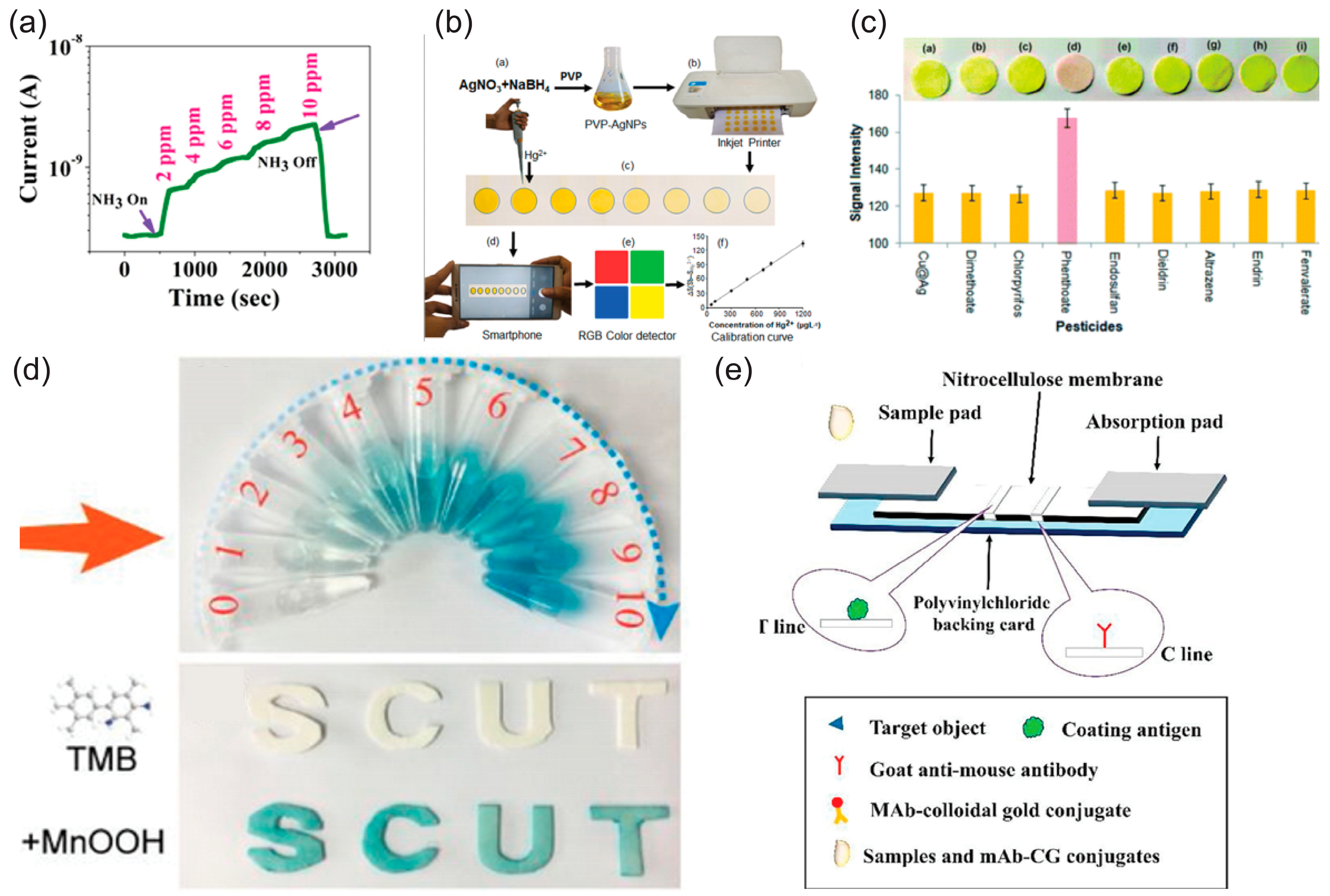
2.1. Pesticide—Heavy Metals Detection
2.2. Physical Sensors
2.3. Humidity Sensors
2.4. Electrochemical Sensors—Biosensors
2.4.1. Glucose Sensors
2.4.2. Cancer Sensors
2.5. μPADs
3. Paper-Based Field-Effect Transistors (PFETs)
3.1. PFETs for Sensing Applications
3.1.1. PFETs as Biosensors
3.1.2. PFETS as Physical Sensors
3.2. PFETs—Analog-Digital Circuits/Memories
4. Detection Techniques in Paper-Based Sensors
4.1. Electrical Detection
4.2. Optical Detection
4.3. Electrochemical Detection
4.4. Hybrid and Integrated Approaches
5. Conclusions—Future Outlook
Funding
Conflicts of Interest
References
- Ramani, V.; Ghosh, D.; Sodhi, M.S. Understanding Systemic Disruption from the Covid-19-Induced Semiconductor Shortage for the Auto Industry. Omega 2022, 113, 102720. [Google Scholar] [CrossRef] [PubMed]
- Marinova, G.I.; Bitri, A.K. Challenges and Opportunities for Semiconductor and Electronic Design Automation Industry in Post-Covid-19 Years. IOP Conf. Ser. Mater. Sci. Eng. 2021, 1208, 012036. [Google Scholar] [CrossRef]
- Casper, H.; Rexford, A.; Riegel, D.; Robinson, A.; Martin, E.; Awwad, M. The Impact of the Computer Chip Supply Shortage. In Proceedings of the International Conference on Industrial Engineering and Operations Management, Bangalore, India, 16–18 August 2021. [Google Scholar]
- Vijay, Y. Material Shortage Reduction at a Semiconductor Equipment Manufacturing Facility Through the Re-Evaluation of Inventory Management Strategies. Master’s Thesis, Massachusetts Institute of Technology, Cambridge, MA, USA, 2017. [Google Scholar]
- Krolikowski, P.M.; Naggert, K. Semiconductor Shortages and Vehicle Production and Prices. Econ. Comment. 2021, 17, 1–7. [Google Scholar] [CrossRef]
- Voas, J.; Kshetri, N.; DeFranco, J.F. Scarcity and Global Insecurity: The Semiconductor Shortage. IT Prof. 2021, 23, 78–82. [Google Scholar] [CrossRef]
- European Commission: Directorate-General for Communication. What is the European Green Deal? Publications Office of the European Union: Luxembourg, 2019. [Google Scholar] [CrossRef]
- Chang, J.S.; Facchetti, A.F.; Reuss, R. A Circuits and Systems Perspective of Organic/Printed Electronics: Review, Challenges, and Contemporary and Emerging Design Approaches. IEEE J. Emerg. Sel. Top. Circuits Syst. 2017, 7, 7–26. [Google Scholar] [CrossRef]
- Suganuma, K. Introduction to Printed Electronics; SpringerBriefs in Electrical and Computer Engineering; Springer: New York, NY, USA, 2014; ISBN 978-1-4614-9624-3. [Google Scholar]
- Khan, Y.; Thielens, A.; Muin, S.; Ting, J.; Baumbauer, C.; Arias, A.C. A New Frontier of Printed Electronics: Flexible Hybrid Electronics. Adv. Mater. 2020, 32, 1905279. [Google Scholar] [CrossRef]
- Cui, Z. Printed Electronics: Materials, Technologies and Applications; John Wiley & Sons Singapore Pte. Ltd: Singapore, 2016; ISBN 978-1-118-92095-4. [Google Scholar]
- Barmpakos, D.; Kaltsas, G. A Review on Humidity, Temperature and Strain Printed Sensors—Current Trends and Future Perspectives. Sensors 2021, 21, 739. [Google Scholar] [CrossRef]
- Hakola, E. Principles of Conventional Printing. In Papermaking Science and Technology: Print Media—Principles, Processes and Quality; Finnish Paper Engineers’ Association: Helsinki, Finland, 2009; pp. 40–87. [Google Scholar]
- De Gans, B.-J.; Duineveld, P.C.; Schubert, U.S. Inkjet Printing of Polymers: State of the Art and Future Developments. Advanced. Adv. Mater. 2004, 16, 203–213. [Google Scholar] [CrossRef]
- Barmpakos, D.; Tsamis, C.; Kaltsas, G. Multi-Parameter Paper Sensor Fabricated by Inkjet-Printed Silver Nanoparticle Ink and PEDOT:PSS. Microelectron. Eng. 2020, 225, 111266. [Google Scholar] [CrossRef]
- Wu, W. Inorganic Nanomaterials for Printed Electronics: A Review. Nanoscale 2017, 9, 7342–7372. [Google Scholar] [CrossRef]
- Anderson, N.; Szorc, N.; Gunasekaran, V.; Joshi, S.; Jursich, G. Highly Sensitive Screen Printed Strain Sensors on Flexible Substrates via Ink Composition Optimization. Sens. Actuators A Phys. 2019, 290, 1–7. [Google Scholar] [CrossRef]
- Gupta, A.A.; Bolduc, A.; Cloutier, S.G.; Izquierdo, R. Aerosol Jet Printing for Printed Electronics Rapid Prototyping. In Proceedings of the 2016 IEEE International Symposium on Circuits and Systems (ISCAS), Montreal, QC, Canada, 22–25 May 2016. [Google Scholar]
- Folgar, C.E.; Suchicital, C.; Priya, S. Solution-Based Aerosol Deposition Process for Synthesis of Multilayer Structures. Mater. Lett. 2011, 65, 1302–1307. [Google Scholar] [CrossRef]
- Kim, C.-Y.; Jung, H.; Choi, H.; Choi, D. Synthesis of One-Dimensional SnO2 Lines by Using Electrohydrodynamic Jet Printing for a NO Gas Sensor. J. Korean Phys. Soc. 2016, 68, 357–362. [Google Scholar] [CrossRef]
- Go, E.-B.; Kim, H.-T.; Kim, C.-Y. Synthesis of One-Dimensional Pillar Arrays by Electrohydrodynamic Jet Printing for Glucose Sensor. J. Biomed. Nanotechnol. 2017, 13, 61–67. [Google Scholar] [CrossRef]
- Belessi, V.; Manolis, G.K.; Vlahopoulos, G.; Philippakopoulou, T.; Steriotis, T.; Koutsioukis, A.; Georgakilas, V. Gravure and Flexography Printing of Highly Conductive Reduced Graphene Oxide Inks. In Proceedings of the 3rd International Printing Technologies Symposium, Istanbul, Turkey, 10–12 October 2019; pp. 180–188. [Google Scholar]
- Szentgyörgyvölgyi, R. Gravure Printing. In Printing on Polymers; Elsevier: Amsterdam, The Netherlands, 2016; pp. 199–215. ISBN 978-0-323-37468-2. [Google Scholar]
- Izdebska, J. Flexographic Printing. In Printing on Polymers Fundamentals and Applications; Elsevier: Amsterdam, The Netherlands, 2016. [Google Scholar]
- Pavlović, Ž.; Dedijer, S.; Draganov, S.; Karlovits, I.; Jurič, I. Offset Printing. In Printing on Polymers; Elsevier: Amsterdam, The Netherlands, 2015; ISBN 978-0-323-37468-2. [Google Scholar]
- Tobjörk, D.; Österbacka, R. Paper Electronics. Adv. Mater. 2011, 23, 1935–1961. [Google Scholar] [CrossRef]
- Liu, H.; Qing, H.; Li, Z.; Han, Y.L.; Lin, M.; Yang, H.; Li, A.; Lu, T.J.; Li, F.; Xu, F. Paper: A Promising Material for Human-Friendly Functional Wearable Electronics. Mater. Sci. Eng. R Rep. 2017, 112, 1–22. [Google Scholar] [CrossRef]
- Xu, Y.; Fei, Q.; Page, M.; Zhao, G.; Ling, Y.; Stoll, S.B.; Yan, Z. Paper-Based Wearable Electronics. iScience 2021, 24, 102736. [Google Scholar] [CrossRef]
- Bhattacharya, G.; Fishlock, S.J.; Hussain, S.; Choudhury, S.; Xiang, A.; Kandola, B.; Pritam, A.; Soin, N.; Roy, S.S.; McLaughlin, J.A. Disposable Paper-Based Biosensors: Optimizing the Electrochemical Properties of Laser-Induced Graphene. ACS Appl. Mater. Interfaces 2022, 14, 31109–31120. [Google Scholar] [CrossRef]
- Monisha; Shrivas, K.; Patle, T.K.; Jamunkar, R.; Jain, V.K.; Banerjee, S.; Kumar, A. Development of Nanomaterials-Fabricated Paper-Based Sensors for theAnalysis of Environmental and Biological Samples: A Review. Curr. Nanosci. 2022, 18, 487–498. [Google Scholar] [CrossRef]
- Nery, E.W.; Kubota, L.T. Sensing Approaches on Paper-Based Devices: A Review. Anal. Bioanal. Chem. 2013, 405, 7573–7595. [Google Scholar] [CrossRef]
- Tortorich, R.P.; Shamkhalichenar, H.; Choi, J.-W. Inkjet-Printed and Paper-Based Electrochemical Sensors. Appl. Sci. 2018, 8, 288. [Google Scholar] [CrossRef]
- Liana, D.D.; Raguse, B.; Gooding, J.J.; Chow, E. Recent Advances in Paper-Based Sensors. Sensors 2012, 12, 11505–11526. [Google Scholar] [CrossRef] [PubMed]
- Meng, F.; Aihaiti, A.; Li, X.; Zhang, W.; Qin, Y.; Zhu, N.; Zhang, M. Functional Graphene Paper from Smart Building to Sensor Application. Biosens. Bioelectron. 2022, 203, 114031. [Google Scholar] [CrossRef]
- Lin, Y.; Gritsenko, D.; Liu, Q.; Lu, X.; Xu, J. Recent Advancements in Functionalized Paper-Based Electronics. ACS Appl. Mater. Interfaces 2016, 8, 20501–20515. [Google Scholar] [CrossRef]
- Zhang, Y.; Zhang, L.; Cui, K.; Ge, S.; Cheng, X.; Yan, M.; Yu, J.; Liu, H. Flexible Electronics Based on Micro/Nanostructured Paper. Adv. Mater. 2018, 30, 1801588. [Google Scholar] [CrossRef]
- Noviana, E.; Ozer, T.; Carrell, C.S.; Link, J.S.; McMahon, C.; Jang, I.; Henry, C.S. Microfluidic Paper-Based Analytical Devices: From Design to Applications. Chem. Rev. 2021, 121, 11835–11885. [Google Scholar] [CrossRef]
- Cate, D.M.; Adkins, J.A.; Mettakoonpitak, J.; Henry, C.S. Recent Developments in Paper-Based Microfluidic Devices. Anal. Chem. 2015, 87, 19–41. [Google Scholar] [CrossRef]
- Singhal, H.R.; Prabhu, A.; Giri Nandagopal, M.S.; Dheivasigamani, T.; Mani, N.K. One-Dollar Microfluidic Paper-Based Analytical Devices: Do-It-Yourself Approaches. Microchem. J. 2021, 165, 106126. [Google Scholar] [CrossRef]
- Samuel, V.R.; Rao, K.J. A Review on Label Free Biosensors. Biosens. Bioelectron X 2022, 11, 100216. [Google Scholar] [CrossRef]
- Suresh Khurd, A.; Kandasubramanian, B. A Systematic Review of Cellulosic Material for Green Electronics Devices. Carbohydr. Polym. Technol. Appl. 2022, 4, 100234. [Google Scholar] [CrossRef]
- Martín-Martín, A.; Orduna-Malea, E.; Thelwall, M.; Delgado López-Cózar, E. Google Scholar, Web of Science, and Scopus: A Systematic Comparison of Citations in 252 Subject Categories. J. Inf. 2018, 12, 1160–1177. [Google Scholar] [CrossRef]
- Mongeon, P.; Paul-Hus, A. The Journal Coverage of Web of Science and Scopus: A Comparative Analysis. Scientometrics 2016, 106, 213–228. [Google Scholar] [CrossRef]
- Gao, H.; Duan, H. 2D and 3D Graphene Materials: Preparation and Bioelectrochemical Applications. Biosens. Bioelectron. 2015, 65, 404–419. [Google Scholar] [CrossRef]
- Yu, Z.; Xu, J.; Gong, H.; Li, Y.; Li, L.; Wei, Q.; Tang, D. Bioinspired Self-Powered Piezoresistive Sensors for Simultaneous Monitoring of Human Health and Outdoor UV Light Intensity. ACS Appl. Mater. Interface 2022, 14, 5101–5111. [Google Scholar] [CrossRef]
- Shrivas, K.; Monisha; Patel, S.; Singh Thakur, S.; Shankar, R. Food Safety Monitoring of the Pesticide Phenthoate Using a Smartphone-Assisted Paper-Based Sensor with Bimetallic Cu@Ag Core–Shell Nanoparticles. Lab. A Chip 2020, 20, 3996–4006. [Google Scholar] [CrossRef]
- Cunha, I.; Martins, J.; Bahubalindruni, P.G.; Carvalho, J.T.; Rodrigues, J.; Rubin, S.; Fortunato, E.; Martins, R.; Pereira, L. Handwritten and Sustainable Electronic Logic Circuits with Fully Printed Paper Transistors. Adv. Mater. Technol. 2021, 6, 2100633. [Google Scholar] [CrossRef]
- Kraft, U.; Zaki, T.; Letzkus, F.; Burghartz, J.N.; Weber, E.; Murmann, B.; Klauk, H. Low-Voltage, High-Frequency Organic Transistors and Unipolar and Complementary Ring Oscillators on Paper. Adv. Electron. Mater. 2019, 5, 1800453. [Google Scholar] [CrossRef]
- Kim, S.-J.; Jeon, D.-B.; Park, J.-H.; Ryu, M.-K.; Yang, J.-H.; Hwang, C.-S.; Kim, G.-H.; Yoon, S.-M. Nonvolatile Memory Thin-Film Transistors Using Biodegradable Chicken Albumen Gate Insulator and Oxide Semiconductor Channel on Eco-Friendly Paper Substrate. ACS Appl. Mater. Interfaces 2015, 7, 4869–4874. [Google Scholar] [CrossRef]
- Jaikang, P.; Paengnakorn, P.; Grudpan, K. Simple Colorimetric Ammonium Assay Employing Well Microplate with Gas Pervaporation and Diffusion for Natural Indicator Immobilized Paper Sensor via Smartphone Detection. Microchem. J. 2020, 152, 104283. [Google Scholar] [CrossRef]
- Vidal, E.; Lorenzetti, A.S.; Aguirre, M.Á.; Canals, A.; Domini, C.E. New, Inexpensive and Simple 3D Printable Device for Nephelometric and Fluorimetric Determination Based on Smartphone Sensing. RSC Adv. 2020, 10, 19713–19719. [Google Scholar] [CrossRef]
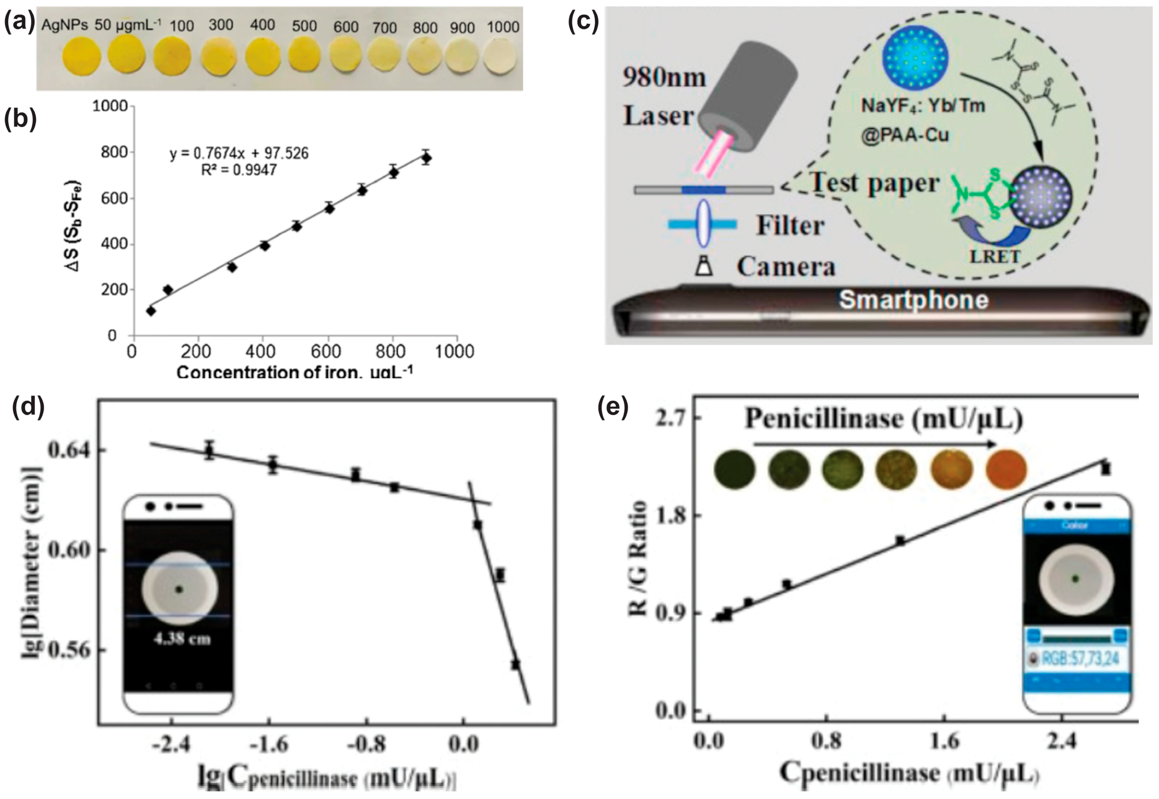
- Shrivas, K.; Monisha; Kant, T.; Karbhal, I.; Kurrey, R.; Sahu, B.; Sinha, D.; Patra, G.K.; Deb, M.K.; Pervez, S. Smartphone Coupled with Paper-Based Chemical Sensor for on-Site Determination of Iron(III) in Environmental and Biological Samples. Anal. Bioanal. Chem. 2020, 412, 1573–1583. [Google Scholar] [CrossRef] [PubMed]
- Mei, Q.; Jing, H.; Li, Y.; Yisibashaer, W.; Chen, J.; Nan Li, B.; Zhang, Y. Smartphone Based Visual and Quantitative Assays on Upconversional Paper Sensor. Biosens. Bioelectron. 2016, 75, 427–432. [Google Scholar] [CrossRef] [PubMed]
- Xu, J.; Chen, X.; Khan, H.; Yang, L. A Dual-Readout Paper-Based Sensor for on-Site Detection of Penicillinase with a Smartphone. Sens. Actuators B Chem. 2021, 335, 129707. [Google Scholar] [CrossRef]
- Biswas, S.K.; Chatterjee, S.; Bandyopadhyay, S.; Kar, S.; Som, N.K.; Saha, S.; Chakraborty, S. Smartphone-Enabled Paper-Based Hemoglobin Sensor for Extreme Point-of-Care Diagnostics. ACS Sens. 2021, 6, 1077–1085. [Google Scholar] [CrossRef]
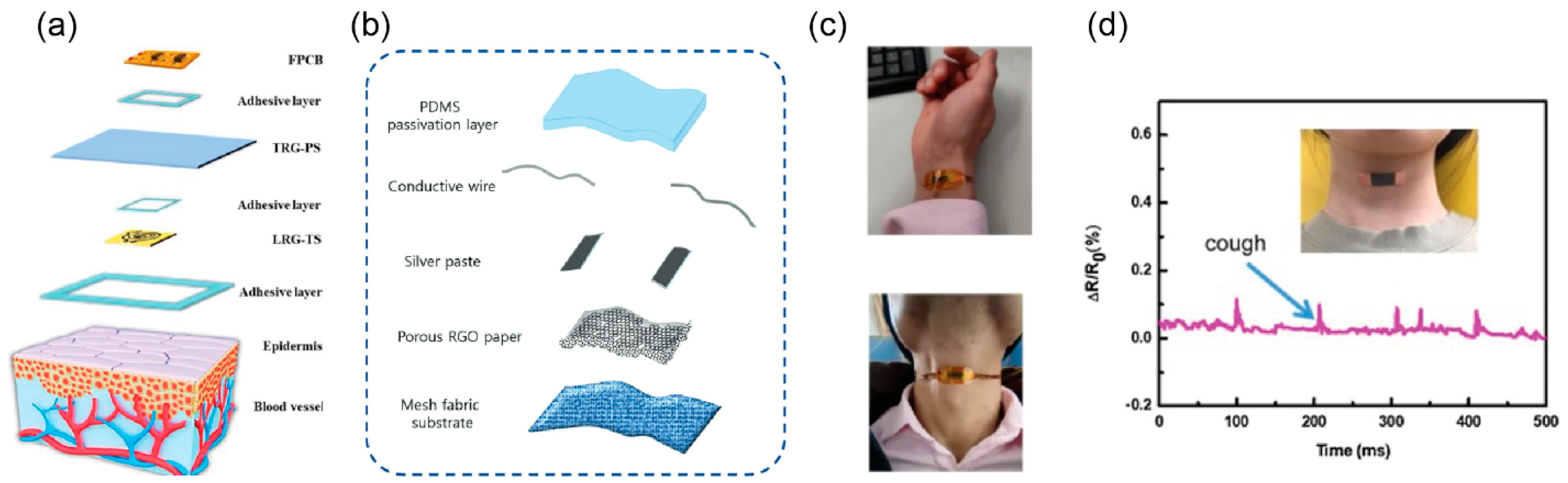
- Zhang, H.; He, R.; Liu, H.; Niu, Y.; Li, Z.; Han, F.; Li, J.; Zhang, X.; Xu, F. A Fully Integrated Wearable Electronic Device with Breathable and Washable Properties for Long-Term Health Monitoring. Sens. Actuators A Phys. 2021, 322, 112611. [Google Scholar] [CrossRef]
- Lee, H.J.; Hong, W.G.; Yang, H.Y.; Ha, D.H.; Jun, Y.; Yun, Y.J. A Wearable Patch Based on Flexible Porous Reduced Graphene Oxide Paper Sensor for Real-Time and Continuous Ultraviolet Radiation Monitoring. Adv. Mater. Technol. 2022, 7, 2100709. [Google Scholar] [CrossRef]
- Li, A.; Cui, C.; Wang, W.; Zhang, Y.; Zhai, J.; Guo, R.; Cheng, C.; Qin, W.; Ren, E.; Xiao, H.; et al. Compressible and Sensitive Aerogels Derived from Graphene/Waste Paper for Wearable Pressure Sensor. J. Mater. Sci. Mater. Electron. 2022, 33, 4388–4399. [Google Scholar] [CrossRef]
- Yang, Y.; Shen, H.; Yang, Z.; Yang, J.; Wang, Z.; Gao, K. Highly Flexible and Sensitive Wearable Strain and Pressure Sensor Based on Porous Graphene Paper for Human Motion. J. Mater. Sci. Mater. Electron. 2022, 33, 17637–17648. [Google Scholar] [CrossRef]
- Yang, Y.; Shen, H.; Yang, Z.; Yang, J.; Wang, Z.; Gao, K. Macroporous and Free-Shape Reduced Graphene Oxide Paper as Sensitive Wearable Pressure and Strain Sensors. Appl. Phys. A Mater. Sci. Process. 2022, 128, 948. [Google Scholar] [CrossRef]
- Qi, X.; Li, X.; Jo, H.; Sideeq Bhat, K.; Kim, S.; An, J.; Kang, J.-W.; Lim, S. Mulberry Paper-Based Graphene Strain Sensor for Wearable Electronics with High Mechanical Strength. Sens. Actuators A Phys. 2020, 301, 111697. [Google Scholar] [CrossRef]
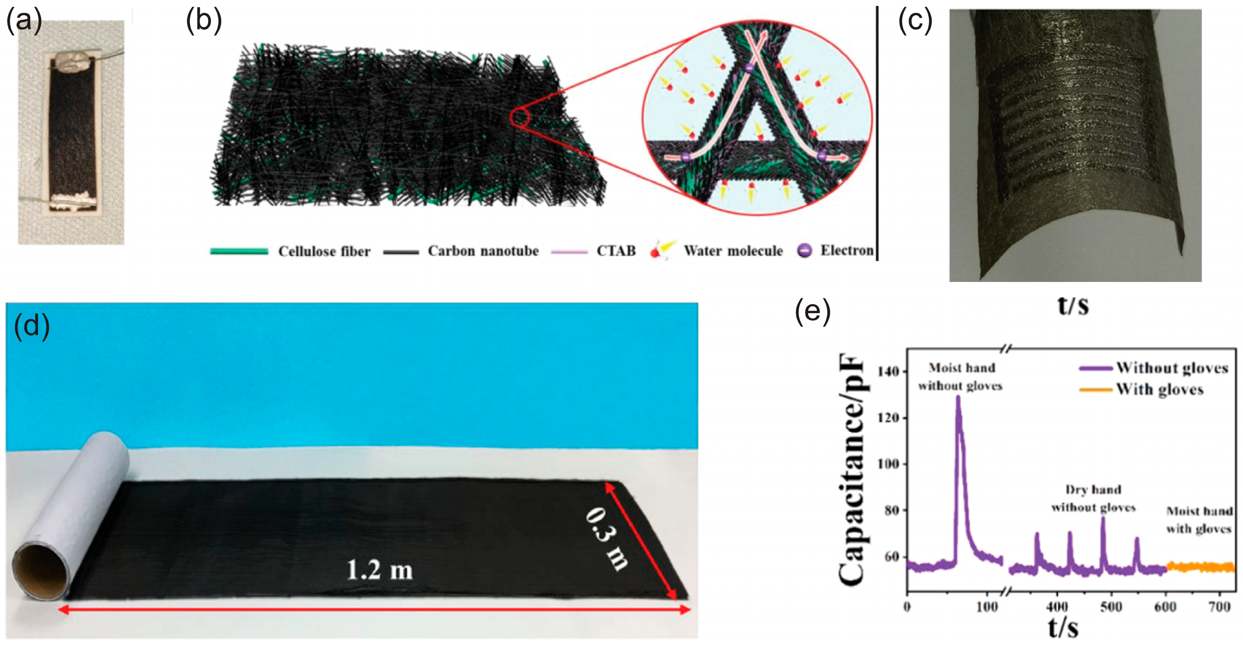
- Liu, H.; Zheng, H.; Xiang, H.; Wang, W.; Wu, H.; Li, Z.; Zhuang, J.; Zhou, H. Paper-Based Wearable Sensors for Humidity and VOC Detection. ACS Sustain. Chem. Eng. 2021, 9, 16937–16945. [Google Scholar] [CrossRef]
- Choo, T.F.; Kok, K.Y.; Saidin, N.U.; Mat Zali, N. Effect of Chemical Treatment and Intrinsic Resistance on the Humidity Sensitivity of Pencil Graphite Sensing Material Coated on Paper Substrate. Sens. Actuators A Phys. 2021, 332, 113085. [Google Scholar] [CrossRef]
- Du, Y.; Li, X.; Zhao, X.; Wang, N.; Li, D. Fabrication and Humidity Sensing of Reduced Graphene Oxide/Polyaniline Composite Film on Flexible Paper Substrate. Sens. Mater. 2022, 34, 2065–2074. [Google Scholar] [CrossRef]
- Kulyk, B.; Silva, B.F.R.; Carvalho, A.F.; Barbosa, P.; Girão, A.V.; Deuermeier, J.; Fernandes, A.J.S.; Figueiredo, F.M.L.; Fortunato, E.; Costa, F.M. Laser-Induced Graphene from Paper by Ultraviolet Irradiation: Humidity and Temperature Sensors. Sens. Mater. 2022, 7, 2101311. [Google Scholar] [CrossRef]
- Mansoori, A.; Ahmad, S.; Sonia; Vashishath, M.; Kumar, D. Low-Cost Inkjet-Printed Humidity Sensor Using Nanoporous Surface on Coated Paper. Sens. Actuators B Chem. 2022, 370, 132389. [Google Scholar] [CrossRef]
- Zhu, P.; Kuang, Y.; Wei, Y.; Li, F.; Ou, H.; Jiang, F.; Chen, G. Electrostatic Self-Assembly Enabled Flexible Paper-Based Humidity Sensor with High Sensitivity and Superior Durability. Chem. Eng. J. 2021, 404, 127105. [Google Scholar] [CrossRef]
- Alrammouz, R.; Podlecki, J.; Vena, A.; Garcia, R.; Abboud, P.; Habchi, R.; Sorli, B. Highly Porous and Flexible Capacitive Humidity Sensor Based on Self-Assembled Graphene Oxide Sheets on a Paper Substrate. Sens. Actuators B Chem. 2019, 298, 126892. [Google Scholar] [CrossRef]
- Zhu, P.; Ou, H.; Kuang, Y.; Hao, L.; Diao, J.; Chen, G. Cellulose Nanofiber/Carbon Nanotube Dual Network-Enabled Humidity Sensor with High Sensitivity and Durability. ACS Appl. Mater. Interfaces 2020, 12, 33229–33238. [Google Scholar] [CrossRef]
- Duan, Z.; Jiang, Y.; Huang, Q.; Wang, S.; Wang, Y.; Pan, H.; Zhao, Q.; Xie, G.; Du, X.; Tai, H. Paper and Carbon Ink Enabled Low-Cost, Eco-Friendly, Flexible, Multifunctional Pressure and Humidity Sensors. Smart Mater. Struct. 2021, 30, 055012. [Google Scholar] [CrossRef]
- Guan, X.; Hou, Z.; Wu, K.; Zhao, H.; Liu, S.; Fei, T.; Zhang, T. Flexible Humidity Sensor Based on Modified Cellulose Paper. Sens. Actuators B Chem. 2021, 339, 129879. [Google Scholar] [CrossRef]
- Wang, Y.; Hou, S.; Li, T.; Jin, S.; Shao, Y.; Yang, H.; Wu, D.; Dai, S.; Lu, Y.; Chen, S.; et al. Flexible Capacitive Humidity Sensors Based on Ionic Conductive Wood-Derived Cellulose Nanopapers. ACS Appl. Mater. Interfaces 2020, 12, 41896–41904. [Google Scholar] [CrossRef] [PubMed]
- Zhang, X.; He, D.; Yang, Q.; Atashbar, M.Z. Rapid, Highly Sensitive, and Highly Repeatable Printed Porous Paper Humidity Sensor. Chem. Eng. J. 2022, 433, 133751. [Google Scholar] [CrossRef]
- Duan, Z.; Jiang, Y.; Yan, M.; Wang, S.; Yuan, Z.; Zhao, Q.; Sun, P.; Xie, G.; Du, X.; Tai, H. Facile, Flexible, Cost-Saving, and Environment-Friendly Paper-Based Humidity Sensor for Multifunctional Applications. ACS Appl. Mater. Interfaces 2019, 11, 21840–21849. [Google Scholar] [CrossRef]
- Ma, H.; Liu, Z.; Lou, J.; Ding, Q.; Jiang, Y.; Li, X.; Han, W. Bacterial Cellulose/MWCNT Coatings for Highly Sensitive and Flexible Paper-Based Humidity Sensors. Cellulose 2023, 30, 1193–1204. [Google Scholar] [CrossRef]
- Rehman, H.M.M.U.; Prasanna, A.P.S.; Rehman, M.M.; Khan, M.; Kim, S.-J.; Kim, W.Y. Edible Rice Paper-Based Multifunctional Humidity Sensor Powered by Triboelectricity. Sustain. Mater. Technol. 2023, 36, e00596. [Google Scholar] [CrossRef]
- Karimov, K.S.; Sulaiman, K.; Ahmad, Z.; Akhmedov, K.M.; Mateen, A. Novel Pressure and Displacement Sensors Based on Carbon Nanotubes. Chin. Phys. B 2015, 24, 018801. [Google Scholar] [CrossRef]
- Wang, C.; Hou, X.; Cui, M.; Yu, J.; Fan, X.; Qian, J.; He, J.; Geng, W.; Mu, J.; Chou, X. An Ultra-Sensitive and Wide Measuring Range Pressure Sensor with Paper-Based CNT Film/Interdigitated Structure. Sci. China Mater. 2020, 63, 403–412. [Google Scholar]
- Chen, J.; Tran, V.-T.; Du, H.; Wang, J.; Chen, C. A Direct-Writing Approach for Fabrication of CNT/Paper-Based Piezoresistive Pressure Sensors for Airflow Sensing. Micromachines 2021, 12, 504. [Google Scholar] [CrossRef]
- Zhang, S.; Li, H.; Yang, Z.; Chen, B.; Li, K.; Lai, X.; Zeng, X. Degradable and Stretchable Bio-Based Strain Sensor for Human Motion Detection. J. Colloid. Interface Sci. 2022, 626, 554–563. [Google Scholar] [CrossRef]
- Thiyagarajan, K.; Rajini, G.K.; Maji, D. Paper-Based Screen Printed MWCNT-PDMS Composite Strain Sensor for Human Motion Monitoring. In Proceedings of the 2019 IEEE 16th India Council International Conference, INDICON 2019—Symposium Proceedings 2019, Rajkot, India, 13–15 December 2019. [Google Scholar]
- Wang, L.; Zhang, M.; Yang, B.; Ding, X.; Tan, J.; Song, S.; Nie, J. Flexible, Robust, and Durable Aramid Fiber/CNT Composite Paper as a Multifunctional Sensor for Wearable Applications. ACS Appl. Mater. Interfaces 2021, 13, 5486–5497. [Google Scholar] [CrossRef]
- Thiyagarajan, K.; Rajini, G.K.; Maji, D. Fully Printed MWCNT Strain Sensor over Paper Substrate for Human Motion Monitoring. Flex. Print. Electron. 2022, 7, 045003. [Google Scholar]
- Yin, Z.; Chen, X.; Chen, Z.; Song, H.; Lv, P.; Xue, M.; Li, H. Superhydrophobic Photocatalytic Self-Cleaning Nanocellulose-Based Strain Sensor for Full-Range Human Motion Monitoring. Adv. Mater. Interfaces 2023, 10, 2300350. [Google Scholar] [CrossRef]
- Yun, T.; Du, J.; Ji, X.; Tao, Y.; Cheng, Y.; Lv, Y.; Lu, J.; Wang, H. Waterproof and Ultrasensitive Paper-Based Wearable Strain/Pressure Sensor from Carbon Black/Multilayer Graphene/Carboxymethyl Cellulose Composite. Carbohydr. Polym. 2023, 313, 120898. [Google Scholar] [CrossRef]
- Tai, H.; Wang, S.; Duan, Z.; Jiang, Y. Evolution of Breath Analysis Based on Humidity and Gas Sensors: Potential and Challenges. Sens. Actuators B Chem. 2020, 318, 128104. [Google Scholar] [CrossRef]
- Maier, D.; Laubender, E.; Basavanna, A.; Schumann, S.; Güder, F.; Urban, G.A.; Dincer, C. Toward Continuous Monitoring of Breath Biochemistry: A Paper-Based Wearable Sensor for Real-Time Hydrogen Peroxide Measurement in Simulated Breath. ACS Sens. 2019, 4, 2945–2951. [Google Scholar] [CrossRef]
- Huang, S.-J.; Immanuel, P.N.; Yen, Y.-K.; Yen, C.-L.; Tseng, C.-E.; Lin, G.-T.; Lin, C.-K.; Huang, Z.-X. Tungsten Disulfide Nanotube-Modified Conductive Paper-Based Chemiresistive Sensor for the Application in Volatile Organic Compounds’ Detection. Sensors 2021, 21, 6121. [Google Scholar] [CrossRef]
- Sarfraz, J.; Rosqvist, E.; Ihalainen, P.; Peltonen, J. Electro-Optical Gas Sensor Consisting of Nanostructured Paper Coating and an Ultrathin Sensing Element. Chemosensors 2019, 7, 23. [Google Scholar] [CrossRef]
- Jemmeli, D.; Marcoccio, E.; Moscone, D.; Dridi, C.; Arduini, F. Highly Sensitive Paper-Based Electrochemical Sensor for Reagent Free Detection of Bisphenol A. Talanta 2020, 216, 120924. [Google Scholar] [CrossRef]
- Das, P.S.; Park, S.H.; Baik, K.Y.; Lee, J.W.; Park, J.Y. Thermally Reduced Graphene Oxide-Nylon Membrane Based Epidermal Sensor Using Vacuum Filtration for Wearable Electrophysiological Signals and Human Motion Monitoring. Carbon. 2020, 158, 386–393. [Google Scholar] [CrossRef]
- Parrilla, M.; Guinovart, T.; Ferré, J.; Blondeau, P.; Andrade, F.J. A Wearable Paper-Based Sweat Sensor for Human Perspiration Monitoring. Adv. Healthc. Mater. 2019, 8, 1900342. [Google Scholar] [CrossRef]
- Ardalan, S.; Hosseinifard, M.; Vosough, M.; Golmohammadi, H. Towards Smart Personalized Perspiration Analysis: An IoT-Integrated Cellulose-Based Microfluidic Wearable Patch for Smartphone Fluorimetric Multi-Sensing of Sweat Biomarkers. Biosens. Bioelectron. 2020, 168, 112450. [Google Scholar] [CrossRef] [PubMed]
- Wang, Q.; Yin, Q.; Fan, Y.; Zhang, L.; Xu, Y.; Hu, O.; Guo, X.; Shi, Q.; Fu, H.; She, Y. Double Quantum Dots-Nanoporphyrin Fluorescence-Visualized Paper-Based Sensors for Detecting Organophosphorus Pesticides. Talanta 2019, 199, 46–53. [Google Scholar] [CrossRef] [PubMed]
- Maity, A.; Raychaudhuri, A.K.; Ghosh, B. High Sensitivity NH3 Gas Sensor with Electrical Readout Made on Paper with Perovskite Halide as Sensor Material. Sci. Rep. 2019, 9, 7777. [Google Scholar] [CrossRef] [PubMed]
- Scandurra, A.; Mirabella, S. Square Wave Anodic Stripping Voltammetry Applied to a Nano-Electrode for Trace Analysis of Pb(II) and Cd(II) Ions in Solution. IEEE Sens. J. 2021, 21, 22134–22142. [Google Scholar] [CrossRef]
- Ercarikci, E.; Alanyalioglu, M. Dual-Functional Graphene-Based Flexible Material for Membrane Filtration and Electrochemical Sensing of Heavy Metal Ions. IEEE Sens. J. 2021, 21, 2468–2475. [Google Scholar] [CrossRef]
- Monisha; Shrivas, K.; Kant, T.; Patel, S.; Devi, R.; Dahariya, N.S.; Pervez, S.; Deb, M.K.; Rai, M.K.; Rai, J. Inkjet-Printed Paper-Based Colorimetric Sensor Coupled with Smartphone for Determination of Mercury (Hg2+). J. Hazard. Mater. 2021, 414, 125440. [Google Scholar] [CrossRef]
- Wang, H.; Da, L.; Yang, L.; Chu, S.; Yang, F.; Yu, S.; Jiang, C. Colorimetric Fluorescent Paper Strip with Smartphone Platform for Quantitative Detection of Cadmium Ions in Real Samples. J. Hazard. Mater. 2020, 392, 122506. [Google Scholar] [CrossRef]
- Huang, L.; Sun, D.-W.; Pu, H.; Wei, Q.; Luo, L.; Wang, J. A Colorimetric Paper Sensor Based on the Domino Reaction of Acetylcholinesterase and Degradable γ-MnOOH Nanozyme for Sensitive Detection of Organophosphorus Pesticides. Sens. Actuators B Chem. 2019, 290, 573–580. [Google Scholar] [CrossRef]
- Lu, Z.; Chen, M.; Liu, T.; Wu, C.; Sun, M.; Su, G.; Wang, X.; Wang, Y.; Yin, H.; Zhou, X.; et al. Machine Learning System To Monitor Hg2+ and Sulfide Using a Polychromatic Fluorescence-Colorimetric Paper Sensor. ACS Appl. Mater. Interfaces 2023, 15, 9800–9812. [Google Scholar] [CrossRef]
- Dong, R.-E.; Kang, P.; Xu, X.-L.; Cai, L.-X.; Guo, Z. Cation-Exchange Strategy for a Colorimetric Paper Sensor: Belt-like ZnSe Nanoframes toward Visual Determination of Heavy Metal Ions. Sens. Actuators B Chem. 2020, 312, 128013. [Google Scholar] [CrossRef]
- Arshad, A.; Wang, H.; Bai, X.; Jiang, R.; Xu, S.; Wang, L. Colorimetric Paper Sensor for Sensitive Detection of Explosive Nitroaromatics Based on Au@Ag Nanoparticles. Spectrochim. Acta-Part. A Mol. Biomol. Spectrosc. 2019, 206, 16–22. [Google Scholar] [CrossRef] [PubMed]
- Wang, Z.; Zhang, J.; Liu, L.; Wu, X.; Kuang, H.; Xu, C.; Xu, L. A Colorimetric Paper-Based Sensor for Toltrazuril and Its Metabolites in Feed, Chicken, and Egg Samples. Food Chem. 2019, 276, 707–713. [Google Scholar] [CrossRef]
- Boobphahom, S.; Ruecha, N.; Rodthongkum, N.; Chailapakul, O.; Remcho, V.T. A Copper Oxide-Ionic Liquid/Reduced Graphene Oxide Composite Sensor Enabled by Digital Dispensing: Non-Enzymatic Paper-Based Microfluidic Determination of Creatinine in Human Blood Serum. Anal. Chim. Acta 2019, 1083, 110–118. [Google Scholar] [CrossRef]
- Lakshmi, G.B.V.S.; Kondal, S.; Dhiman, T.K.; Gupta, P.K.; Solanki, P.R. A Disposable, Environment—Friendly, Cost-Effective Paper Based Electrochemical Cholesterol Biosensor Fabricated Using Screen Printing Technique. ECS Trans. 2022, 107, 18113–18121. [Google Scholar]
- Kala, D.; Sharma, T.K.; Gupta, S.; Verma, V.; Thakur, A.; Kaushal, A.; Trukhanov, A.V.; Trukhanov, S.V. Graphene Oxide Nanoparticles Modified Paper Electrode as a Biosensing Platform for Detection of the Htra Gene of o. Tsutsugamushi. Sensors 2021, 21, 4366. [Google Scholar] [CrossRef]
- Parrilla, M.; Vanhooydonck, A.; Watts, R.; De Wael, K. Wearable Wristband-Based Electrochemical Sensor for the Detection of Phenylalanine in Biofluids. Biosens. Bioelectron. 2022, 197, 113764. [Google Scholar] [CrossRef]
- Mousavi, S.M.; Behbudi, G.; Hashemi, S.A.; Babapoor, A.; Chiang, W.-H.; Ramakrishna, S.; Rahman, M.M.; Lai, C.W.; Gholami, A.; Omidifar, N.; et al. Recent Progress in Electrochemical Detection of Human Papillomavirus (HPV) via Graphene-Based Nanosensors. J. Sens. 2021, 2021, 6673483. [Google Scholar] [CrossRef]
- Chen, R.; Peng, X.; Song, Y.; Du, Y. A Paper-Based Electrochemical Sensor Based on PtNP/COFTFPB−DHzDS@rGO for Sensitive Detection of Furazolidone. Biosensors 2022, 12, 904. [Google Scholar] [CrossRef]
- Karuppiah, S.; Mishra, N.C.; Tsai, W.-C.; Liao, W.-S.; Chou, C.-F. Ultrasensitive and Low-Cost Paper-Based Graphene Oxide Nanobiosensor for Monitoring Water-Borne Bacterial Contamination. ACS Sens. 2021, 6, 3214–3223. [Google Scholar] [CrossRef]
- Ge, R.; Lin, X.; Dai, H.; Wei, J.; Jiao, T.; Chen, Q.; Oyama, M.; Chen, Q.; Chen, X. Photoelectrochemical Sensors with Near-Infrared-Responsive Reduced Graphene Oxide and MoS2for Quantification of Escherichia Coli O157:H7. ACS Appl. Mater. Interfaces 2022, 14, 41649–41658. [Google Scholar] [CrossRef]
- Liu, Y.; Wu, Y.; Wang, L.; Zhu, L.; Dong, Y.; Xu, W. A Ratiometric Dual-Fluorescent Paper-Based Synthetic Biosensor for Visual Detection of Tetracycline on-Site. J. Hazard. Mater. 2024, 467, 133647. [Google Scholar] [CrossRef] [PubMed]
- Scognamiglio, V.; Arduini, F. The Technology Tree in the Design of Glucose Biosensors. TrAC—Trends Anal. Chem. 2019, 120, 115642. [Google Scholar] [CrossRef]
- Yang, H.; Bao, J.; Qi, Y.; Zhao, J.; Hu, Y.; Wu, W.; Wu, X.; Zhong, D.; Huo, D.; Hou, C. A Disposable and Sensitive Non-Enzymatic Glucose Sensor Based on 3D Graphene/Cu2O Modified Carbon Paper Electrode. Anal. Chim. Acta 2020, 1135, 12–19. [Google Scholar] [CrossRef]
- Zhao, A.; Zhang, Z.; Zhang, P.; Xiao, S.; Wang, L.; Dong, Y.; Yuan, H.; Li, P.; Sun, Y.; Jiang, X.; et al. 3D Nanoporous Gold Scaffold Supported on Graphene Paper: Freestanding and Flexible Electrode with High Loading of Ultrafine PtCo Alloy Nanoparticles for Electrochemical Glucose Sensing. Anal. Chim. Acta 2016, 938, 63–71. [Google Scholar] [CrossRef]
- Scandurra, A.; Censabella, M.; Boscarino, S.; Condorelli, G.G.; Grimaldi, M.G.; Ruffino, F. Fabrication of Cu(II) Oxide-Hydroxide Nanostructures onto Graphene Paper by Laser and Thermal Processes for Sensitive Nano-Electrochemical Sensing of Glucose. Nanotechnology 2022, 33, 045501. [Google Scholar] [CrossRef]
- Wang, B.; Wu, Y.; Chen, Y.; Weng, B.; Li, C. Flexible Paper Sensor Fabricated via in Situ Growth of Cu Nanoflower on RGO Sheets towards Amperometrically Non-Enzymatic Detection of Glucose. Sens. Actuators B Chem. 2017, 238, 802–808. [Google Scholar] [CrossRef]
- Scandurra, A.; Ruffino, F.; Sanzaro, S.; Grimaldi, M.G. Laser and Thermal Dewetting of Gold Layer onto Graphene Paper for Non-Enzymatic Electrochemical Detection of Glucose and Fructose. Sens. Actuators B Chem. 2019, 301, 127113. [Google Scholar] [CrossRef]
- Chaiyo, S.; Mehmeti, E.; Siangproh, W.; Hoang, T.L.; Nguyen, H.P.; Chailapakul, O.; Kalcher, K. Non-Enzymatic Electrochemical Detection of Glucose with a Disposable Paper-Based Sensor Using a Cobalt Phthalocyanine–Ionic Liquid–Graphene Composite. Biosens. Bioelectron. 2018, 102, 113–120. [Google Scholar] [CrossRef]
- Tam, T.V.; Hur, S.H.; Chung, J.S.; Choi, W.M. Novel Paper- and Fiber Optic-Based Fluorescent Sensor for Glucose Detection Using Aniline-Functionalized Graphene Quantum Dots. Sens. Actuators B Chem 2021, 329, 129250. [Google Scholar] [CrossRef]
- Razavi, F.; Khajehsharifi, H. Paper-Based Electrochemical Sensor with a Commercial Glucose Meter to Determine L-Cysteine by Graphene Electrode and Ag-Doped Silica Nanoporous SBA-16. J. Iran. Chem. Soc. 2022, 19, 4349–4357. [Google Scholar] [CrossRef]
- He, W.; Sun, Y.; Xi, J.; Abdurhman, A.A.M.; Ren, J.; Duan, H. Printing Graphene-Carbon Nanotube-Ionic Liquid Gel on Graphene Paper: Towards Flexible Electrodes with Efficient Loading of PtAu Alloy Nanoparticles for Electrochemical Sensing of Blood Glucose. Anal. Chim. Acta 2016, 903, 61–68. [Google Scholar] [CrossRef] [PubMed]
- Zheng, W.; Li, Y.; Hu, L.; Lee, L.Y.S. Use of Carbon Supports with Copper Ion as a Highly Sensitive Non-Enzymatic Glucose Sensor. Sens. Actuators B Chem. 2019, 282, 187–196. [Google Scholar] [CrossRef]
- Rewatkar, P.; Goel, S. Paper-Based Membraneless Co-Laminar Microfluidic Glucose Biofuel Cell with MWCNT-Fed Bucky Paper Bioelectrodes. IEEE Trans. Nanobiosci 2018, 17, 374–379. [Google Scholar] [CrossRef] [PubMed]
- Cao, L.; Han, G.-C.; Xiao, H.; Chen, Z.; Fang, C. A Novel 3D Paper-Based Microfluidic Electrochemical Glucose Biosensor Based on rGO-TEPA/PB Sensitive Film. Anal. Chim. Acta 2020, 1096, 34–43. [Google Scholar] [CrossRef]
- Cai, S.; Xu, C.; Jiang, D.; Yuan, M.; Zhang, Q.; Li, Z.; Wang, Y. Air-Permeable Electrode for Highly Sensitive and Noninvasive Glucose Monitoring Enabled by Graphene Fiber Fabrics. Nano Energy 2022, 93, 106904. [Google Scholar] [CrossRef]
- Darabdhara, G.; Boruah, P.K.; Das, M.R. Colorimetric Determination of Glucose in Solution and via the Use of a Paper Strip by Exploiting the Peroxidase and Oxidase Mimicking Activity of Bimetallic Cu-Pd Nanoparticles Deposited on Reduced Graphene Oxide, Graphitic Carbon Nitride, or MoS2 Nanosheets. Microchim. Acta 2019, 186, 13. [Google Scholar]
- Fakhri, N.; Salehnia, F.; Mohammad Beigi, S.; Aghabalazadeh, S.; Hosseini, M.; Ganjali, M.R. Enhanced Peroxidase-like Activity of Platinum Nanoparticles Decorated on Nickel- and Nitrogen-Doped Graphene Nanotubes: Colorimetric Detection of Glucose. Microchim. Acta 2019, 186, 385. [Google Scholar] [CrossRef]
- Roekmono; Hadi, H.; Imtihani, H.N.; Wahyuono, R.A. Paper-Based Biosensor for Glucose and Paracetamol Sensing Using Chitosan/Graphene Oxide Modified Electrode. Int. J. Drug Deliv. Technol. 2020, 10, 295–300. [Google Scholar]
- Ahmadi, A.; Khoshfetrat, S.M.; Kabiri, S.; Fotouhi, L.; Dorraji, P.S.; Omidfar, K. Impedimetric Paper-Based Enzymatic Biosensor Using Electrospun Cellulose Acetate Nanofiber and Reduced Graphene Oxide for Detection of Glucose from Whole Blood. IEEE Sens. J. 2021, 21, 9210–9217. [Google Scholar] [CrossRef]
- Niamsi, W.; Larpant, N.; Kalambate, P.K.; Primpray, V.; Karuwan, C.; Rodthongkum, N.; Laiwattanapaisal, W. Paper-Based Screen-Printed Ionic-Liquid/Graphene Electrode Integrated with Prussian Blue/MXene Nanocomposites Enabled Electrochemical Detection for Glucose Sensing. Biosensors 2022, 12, 852. [Google Scholar] [CrossRef]
- Gokoglan, T.C.; Kesik, M.; Soylemez, S.; Yuksel, R.; Unalan, H.E.; Toppare, L. Paper Based Glucose Biosensor Using Graphene Modified with a Conducting Polymer and Gold Nanoparticles. J. Electrochem. Soc. 2017, 164, G59–G64. [Google Scholar] [CrossRef]
- Yoo, S.; Min, K.; Tae, G.; Su Han, M. A Long-Term Stable Paper-Based Glucose Sensor Using a Glucose Oxidase-Loaded, Mn 2 BPMP-Conjugated Nanocarrier with a Smartphone Readout. Nanoscale 2021, 13, 4467–4474. [Google Scholar] [CrossRef] [PubMed]
- Khachornsakkul, K.; Rybicki, F.J.; Sonkusale, S. Nanomaterials Integrated with Microfluidic Paper-Based Analytical Devices for Enzyme-Free Glucose Quantification. Talanta 2023, 260, 124538. [Google Scholar] [CrossRef] [PubMed]
- Cheng, Y.; Feng, S.; Ning, Q.; Li, T.; Xu, H.; Sun, Q.; Cui, D.; Wang, K. Dual-Signal Readout Paper-Based Wearable Biosensor with a 3D Origami Structure for Multiplexed Analyte Detection in Sweat. Microsyst. Nanoeng. 2023, 9, 36. [Google Scholar] [CrossRef]
- Ortiz-Gómez, I.; Toral-López, V.; Romero, F.J.; de Orbe-Payá, I.; García, A.; Rodríguez, N.; Capitán-Vallvey, L.F.; Morales, D.P.; Salinas-Castillo, A. In Situ Synthesis of Fluorescent Silicon Nanodots for Determination of Total Carbohydrates in a Paper Microfluidic Device Combined with Laser Prepared Graphene Heater. Sens. Actuators B Chem. 2021, 332, 129506. [Google Scholar] [CrossRef]
- Niroula, J.; Premaratne, G.; Krishnan, S. Lab-on-Paper Aptasensor for Label-Free Picomolar Detection of a Pancreatic Hormone in Serum. Biosens. Bioelectron X 2022, 10, 100114. [Google Scholar] [CrossRef]
- Yang, Y.; Ji, W.; Yin, Y.; Wang, N.; Wu, W.; Zhang, W.; Pei, S.; Liu, T.; Tao, C.; Zheng, B.; et al. Catalytic Modification of Porous Two-Dimensional Ni-MOFs on Portable Electrochemical Paper-Based Sensors for Glucose and Hydrogen Peroxide Detection. Biosensors 2023, 13, 508. [Google Scholar] [CrossRef]
- Zhou, J.; Zheng, Y.; Liu, J.; Bing, X.; Hua, J.; Zhang, H. A Paper-Based Detection Method of Cancer Cells Using the Photo-Thermal Effect of Nanocomposite. J. Pharm. Biomed. Anal. 2016, 117, 333–337. [Google Scholar] [CrossRef]
- Fan, Y.; Shi, S.; Ma, J.; Guo, Y. A Paper-Based Electrochemical Immunosensor with Reduced Graphene Oxide/Thionine/Gold Nanoparticles Nanocomposites Modification for the Detection of Cancer Antigen 125. Biosens. Bioelectron. 2019, 135, 1–7. [Google Scholar] [CrossRef]
- Fan, Y.; Liu, J.; Wang, Y.; Luo, J.; Xu, H.; Xu, S.; Cai, X. A Wireless Point-of-Care Testing System for the Detection of Neuron-Specific Enolase with Microfluidic Paper-Based Analytical Devices. Biosens. Bioelectron. 2017, 95, 60–66. [Google Scholar] [CrossRef]
- Wang, Y.; Sun, S.; Luo, J.; Xiong, Y.; Ming, T.; Liu, J.; Ma, Y.; Yan, S.; Yang, Y.; Yang, Z.; et al. Low Sample Volume Origami-Paper-Based Graphene-Modified Aptasensors for Label-Free Electrochemical Detection of Cancer Biomarker-EGFR. Microsyst. Nanoeng. 2020, 6, 32. [Google Scholar] [CrossRef]
- Li, L.; Zhang, L.; Yu, J.; Ge, S.; Song, X. All-Graphene Composite Materials for Signal Amplification toward Ultrasensitive Electrochemical Immunosensing of Tumor Marker. Biosens. Bioelectron. 2015, 71, 108–114. [Google Scholar] [CrossRef] [PubMed]
- Liang, L.; Su, M.; Li, L.; Lan, F.; Yang, G.; Ge, S.; Yu, J.; Song, X. Aptamer-Based Fluorescent and Visual Biosensor for Multiplexed Monitoring of Cancer Cells in Microfluidic Paper-Based Analytical Devices. Sens. Actuators B Chem. 2016, 229, 347–354. [Google Scholar] [CrossRef]
- Prasad, K.S.; Cao, X.; Gao, N.; Jin, Q.; Sanjay, S.T.; Henao-Pabon, G.; Li, X. A Low-Cost Nanomaterial-Based Electrochemical Immunosensor on Paper for High-Sensitivity Early Detection of Pancreatic Cancer. Sens. Actuators B Chem. 2020, 305, 127516. [Google Scholar] [CrossRef]
- Bahavarnia, F.; Saadati, A.; Hassanpour, S.; Hasanzadeh, M.; Shadjou, N.; Hassanzadeh, A. Paper Based Immunosensing of Ovarian Cancer Tumor Protein CA 125 Using Novel Nano-Ink: A New Platform for Efficient Diagnosis of Cancer and Biomedical Analysis Using Microfluidic Paper-Based Analytical Devices (μPAD). Int. J. Biol. Macromol. 2019, 138, 744–754. [Google Scholar] [CrossRef]
- Kumar, S.; Kumar, S.; Srivastava, S.; Yadav, B.K.; Lee, S.H.; Sharma, J.G.; Doval, D.C.; Malhotra, B.D. Reduced Graphene Oxide Modified Smart Conducting Paper for Cancer Biosensor. Biosens. Bioelectron. 2015, 73, 114–122. [Google Scholar] [CrossRef]
- Yen, Y.-K.; Chao, C.-H.; Yeh, Y.-S. A Graphene-PEDOT:PSS Modified Paper-Based Aptasensor for Electrochemical Impedance Spectroscopy Detection of Tumor Marker. Sensors 2020, 20, 1372. [Google Scholar] [CrossRef]
- Kumar, S.; Umar, M.; Saifi, A.; Kumar, S.; Augustine, S.; Srivastava, S.; Malhotra, B.D. Electrochemical Paper Based Cancer Biosensor Using Iron Oxide Nanoparticles Decorated PEDOT:PSS. Anal. Chim. Acta 2019, 1056, 135–145. [Google Scholar] [CrossRef]
- Ji, S.; Lee, M.; Kim, D. Detection of Early Stage Prostate Cancer by Using a Simple Carbon Nanotube@paper Biosensor. Biosens. Bioelectron. 2018, 102, 345–350. [Google Scholar] [CrossRef]
- Linh, V.T.N.; Kim, H.; Lee, M.-Y.; Mun, J.; Kim, Y.; Jeong, B.-H.; Park, S.-G.; Kim, D.-H.; Rho, J.; Jung, H.S. 3D Plasmonic Hexaplex Paper Sensor for Label-Free Human Saliva Sensing and Machine Learning-Assisted Early-Stage Lung Cancer Screening. Biosens. Bioelectron. 2024, 244, 115779. [Google Scholar] [CrossRef]
- Carrell, C.; Kava, A.; Nguyen, M.; Menger, R.; Munshi, Z.; Call, Z.; Nussbaum, M.; Henry, C. Beyond the Lateral Flow Assay: A Review of Paper-Based Microfluidics. Microelectron. Eng. 2019, 206, 45–54. [Google Scholar] [CrossRef]
- Kim, T.H.; Hahn, Y.K.; Kim, M.S. Recent Advances of Fluid Manipulation Technologies in Microfluidic Paper-Based Analytical Devices (μPADs) toward Multi-Step Assays. Micromachines 2020, 11, 269. [Google Scholar] [CrossRef]
- Selvakumar, B.; Kathiravan, A. Sensory Materials for Microfluidic Paper Based Analytical Devices—A Review. Talanta 2021, 235, 122733. [Google Scholar] [CrossRef]
- Nadar, S.S.; Patil, P.D.; Tiwari, M.S.; Ahirrao, D.J. Enzyme Embedded Microfluidic Paper-Based Analytic Device (μPAD): A Comprehensive Review. Crit. Rev. Biotechnol. 2021, 41, 1046–1080. [Google Scholar] [CrossRef]
- Aghababaie, M.; Foroushani, E.S.; Changani, Z.; Gounani, Z.; Mobarakeh, M.S.; Hadady, H.; Khedri, M.; Maleki, R.; Asadnia, M.; Razmjou, A. Recent Advances In the Development of Enzymatic Paper-Based Microfluidic Biosensors. Biosens. Bioelectron. 2023, 226, 115131. [Google Scholar] [CrossRef]
- Chaiyo, S.; Apiluk, A.; Siangproh, W.; Chailapakul, O. High Sensitivity and Specificity Simultaneous Determination of Lead, Cadmium and Copper Using μPAD with Dual Electrochemical and Colorimetric Detection. Sens. Actuators B Chem. 2016, 233, 540–549. [Google Scholar] [CrossRef]
- Lam, T.; Devadhasan, J.P.; Howse, R.; Kim, J. A Chemically Patterned Microfluidic Paper-Based Analytical Device (C-µPAD) for Point-of-Care Diagnostics. Sci. Rep. 2017, 7, 1188. [Google Scholar] [CrossRef]
- Mercan, Ö.B.; Kılıç, V.; Şen, M. Machine Learning-Based Colorimetric Determination of Glucose in Artificial Saliva with Different Reagents Using a Smartphone Coupled μPAD. Sens. Actuators B Chem. 2021, 329, 129037. [Google Scholar] [CrossRef]
- Fiore, L.; Mazzaracchio, V.; Serani, A.; Fabiani, G.; Fabiani, L.; Volpe, G.; Moscone, D.; Bianco, G.M.; Occhiuzzi, C.; Marrocco, G.; et al. Microfluidic Paper-Based Wearable Electrochemical Biosensor for Reliable Cortisol Detection in Sweat. Sens. Actuators B Chem. 2023, 379, 133258. [Google Scholar] [CrossRef]
- Smith, J.; Hamilton, R.; McCulloch, I.; Heeney, M.; Anthony, J.E.; Bradley, D.D.C.; Anthopoulos, T.D. High Mobility P-Channel Organic Field Effect Transistors on Flexible Substrates Using a Polymer-Small Molecule Blend. Synth. Met. 2009, 159, 2365–2367. [Google Scholar] [CrossRef]
- Fleischhaker, F.; Wloka, V.; Hennig, I. ZnO Based Field-Effect Transistors (FETs): Solution-Processable at Low Temperatures on Flexible Substrates. J. Mater. Chem. 2010, 20, 6622–6625. [Google Scholar] [CrossRef]
- Lee, G.-H.; Yu, Y.-J.; Cui, X.; Petrone, N.; Lee, C.-H.; Choi, M.S.; Lee, D.-Y.; Lee, C.; Yoo, W.J.; Watanabe, K.; et al. Flexible and Transparent MoS2 Field-Effect Transistors on Hexagonal Boron Nitride-Graphene Heterostructures. ACS Nano 2013, 7, 7931–7936. [Google Scholar] [CrossRef] [PubMed]
- Thiburce, Q.; Campbell, A.J. Low-Voltage Polyelectrolyte-Gated Polymer Field-Effect Transistors Gravure Printed at High Speed on Flexible Plastic Substrates. Adv. Electron. Mater. 2017, 3, 1600421. [Google Scholar] [CrossRef]
- Koutsiaki, C.; Kaimakamis, T.; Zachariadis, A.; Papamichail, A.; Kamaraki, C.; Fachouri, S.; Gravalidis, C.; Laskarakis, A.; Logothetidis, S. Efficient Combination of Roll-to-Roll Compatible Techniques towards the Large Area Deposition of a Polymer Dielectric Film and the Solution-Processing of an Organic Semiconductor for the Field-Effect Transistors Fabrication on Plastic Substrate. Org. Electron. 2019, 73, 231–239. [Google Scholar] [CrossRef]
- Zschieschang, U.; Waizmann, U.; Weis, J.; Borchert, J.W.; Klauk, H. Nanoscale Flexible Organic Thin-Film Transistors. Sci. Adv. 2022, 8, eabm9845. [Google Scholar] [CrossRef]
- Zschieschang, U.; Klauk, H. Organic Transistors on Paper: A Brief Review. J. Mater. Chem. C 2019, 7, 5522–5533. [Google Scholar] [CrossRef]
- Bushra, K.A.; Prasad, K.S. Paper-Based Field-Effect Transistor Sensors. Talanta 2022, 239, 123085. [Google Scholar] [CrossRef]
- Cho, W.-J.; Lim, C.-M. Sensing Properties of Separative Paper-Based Extended-Gate Ion-Sensitive Field-Effect Transistor for Cost Effective pH Sensor Applications. Solid-State Electron. 2018, 140, 96–99. [Google Scholar] [CrossRef]
- Wang, H.; Chen, R.; Zhang, F.; Yu, Z.; Wang, Y.; Tang, Z.; Yang, L.; Tang, X.; Xiong, B. Superhydrophobic Paper-Based Microfluidic Field-Effect Transistor Biosensor Functionalized with Semiconducting Single-Walled Carbon Nanotube and DNAzyme for Hypocalcemia Diagnosis. Int. J. Mol. Sci. 2022, 23, 7799. [Google Scholar] [CrossRef]
- Sahatiya, P.; Badhulika, S. Wireless, Smart, Human Motion Monitoring Using Solution Processed Fabrication of Graphene–MoS2 Transistors on Paper. Adv. Electron. Mater. 2018, 4, 1700388. [Google Scholar] [CrossRef]
- Kanaparthi, S.; Badhulika, S. Solvent-Free Fabrication of a Biodegradable All-Carbon Paper Based Field Effect Transistor for Human Motion Detection through Strain Sensing. Green. Chem. 2016, 18, 3640–3646. [Google Scholar] [CrossRef]
- Grau, G.; Kitsomboonloha, R.; Swisher, S.L.; Kang, H.; Subramanian, V. Printed Transistors on Paper: Towards Smart Consumer Product Packaging. Adv. Funct. Mater. 2014, 24, 5067–5074. [Google Scholar] [CrossRef]
- Trifunovic, M.; Sberna, P.M.; Shimoda, T.; Ishihara, R. Solution-Based Polycrystalline Silicon Transistors Produced on a Paper Substrate. npj Flex. Electron. 2017, 1, 1–6. [Google Scholar] [CrossRef]
- Bhatt, K.; Kumar, S.; Tripathi, C.C. High-Performance Ultra-Low Leakage Current Graphene-Based Screen-Printed Field-Effect Transistor on Paper Substrate. Pramana-J. Phys. 2020, 94, 31. [Google Scholar] [CrossRef]
- Nketia-Yawson, B.; Noh, Y.-Y. Recent Progress on High-Capacitance Polymer Gate Dielectrics for Flexible Low-Voltage Transistors. Adv. Funct. Mater. 2018, 28, 1802201. [Google Scholar] [CrossRef]
- Matsui, H.; Takeda, Y.; Tokito, S. Flexible and Printed Organic Transistors: From Materials to Integrated Circuits. Org. Electron. 2019, 75, 105432. [Google Scholar] [CrossRef]
- Chen, S.; Surendran, A.; Wu, X.; Lee, S.Y.; Stephen, M.; Leong, W.L. Recent Technological Advances in Fabrication and Application of Organic Electrochemical Transistors. Adv. Mater. Technol. 2020, 5, 2000523. [Google Scholar] [CrossRef]
- Wang, C.-Y.; Fuentes-Hernandez, C.; Chou, W.-F.; Kippelen, B. Top-Gate Organic Field-Effect Transistors Fabricated on Paper with High Operational Stability. Org. Electron. 2017, 41, 340–344. [Google Scholar] [CrossRef]
- Qian, C.; Sun, J.; Yang, J.; Gao, Y. Flexible Organic Field-Effect Transistors on Biodegradable Cellulose Paper with Efficient Reusable Ion Gel Dielectrics. RSC Adv. 2015, 5, 14567–14574. [Google Scholar] [CrossRef]
- Liu, N.; Yun, K.N.; Yu, H.-Y.; Shim, J.H.; Lee, C.J. High-Performance Carbon Nanotube Thin-Film Transistors on Flexible Paper Substrates. Appl. Phys. Lett. 2015, 106, 103106. [Google Scholar] [CrossRef]
- Hyun, W.J.; Secor, E.B.; Rojas, G.A.; Hersam, M.C.; Francis, L.F.; Frisbie, C.D. All-Printed, Foldable Organic Thin-Film Transistors on Glassine Paper. Adv. Mater. 2015, 27, 7058–7064. [Google Scholar] [CrossRef] [PubMed]
- Jiang, S.; Feng, P.; Yang, Y.; Du, P.; Shi, Y.; Wan, Q. Flexible Low-Voltage In–Zn–O Homojunction TFTs With Beeswax Gate Dielectric on Paper Substrates. IEEE Electron. Device Lett. 2016, 37, 287–290. [Google Scholar] [CrossRef]
- Liu, H.; Li, J.; Tan, R. Flexible In2O3 Nanowire Transistors on Paper Substrates. IEEE J. Electron. Devices Soc. 2017, 5, 141–144. [Google Scholar] [CrossRef]
- Wan, Q.; Dattoli, E.N.; Fung, W.Y.; Guo, W.; Chen, Y.; Pan, X.; Lu, W. High-Performance Transparent Conducting Oxide Nanowires. Nano Lett. 2006, 6, 2909–2915. [Google Scholar] [CrossRef]
- Liu, H.; Sun, J.; Jiang, J.; Tang, Q.; Wan, Q. Ultralow-Voltage Transparent $\hboxIn_2 \hboxO_3$ Nanowire Electric-Double-Layer Transistors. IEEE Electron. Device Lett. 2011, 32, 315–317. [Google Scholar] [CrossRef]
- Park, S.; Akinwande, D. First Demonstration of High Performance 2D Monolayer Transistors on Paper Substrates. In Proceedings of the Technical Digest—International Electron Devices Meeting, IEDM, San Francisco, CA, USA, 2–6 December 2017. [Google Scholar]
- Shin, H.; Roh, J.; Song, J.; Roh, H.; Kang, C.-M.; Lee, T.; Park, G.; An, K.; Kim, J.Y.; Kim, H.; et al. Highly Stable Organic Transistors on Paper Enabled by a Simple and Universal Surface Planarization Method. Adv. Mater. Interfaces 2019, 6, 1801731. [Google Scholar] [CrossRef]
- Carvalho, J.T.; Dubceac, V.; Grey, P.; Cunha, I.; Fortunato, E.; Martins, R.; Clausner, A.; Zschech, E.; Pereira, L. Fully Printed Zinc Oxide Electrolyte-Gated Transistors on Paper. Nanomaterials 2019, 9, 169. [Google Scholar] [CrossRef]
- Morais, R.; Vieira, D.H.; Gaspar, C.; Pereira, L.; Martins, R.; Alves, E.N. Influence of Paper Surface Characteristics on Fully Inkjet Printed PEDOT:PSS-Based Electrochemical Transistors. Semicond. Sci. Technol. 2021, 36, 125005. [Google Scholar] [CrossRef]
- Cagang, A.A.; Abidi, I.H.; Tyagi, A.; Hu, J.; Xu, F.; Lu, T.J.; Luo, Z. Graphene-Based Field Effect Transistor in Two-Dimensional Paper Networks. Anal. Chim. Acta 2016, 917, 101–106. [Google Scholar] [CrossRef]
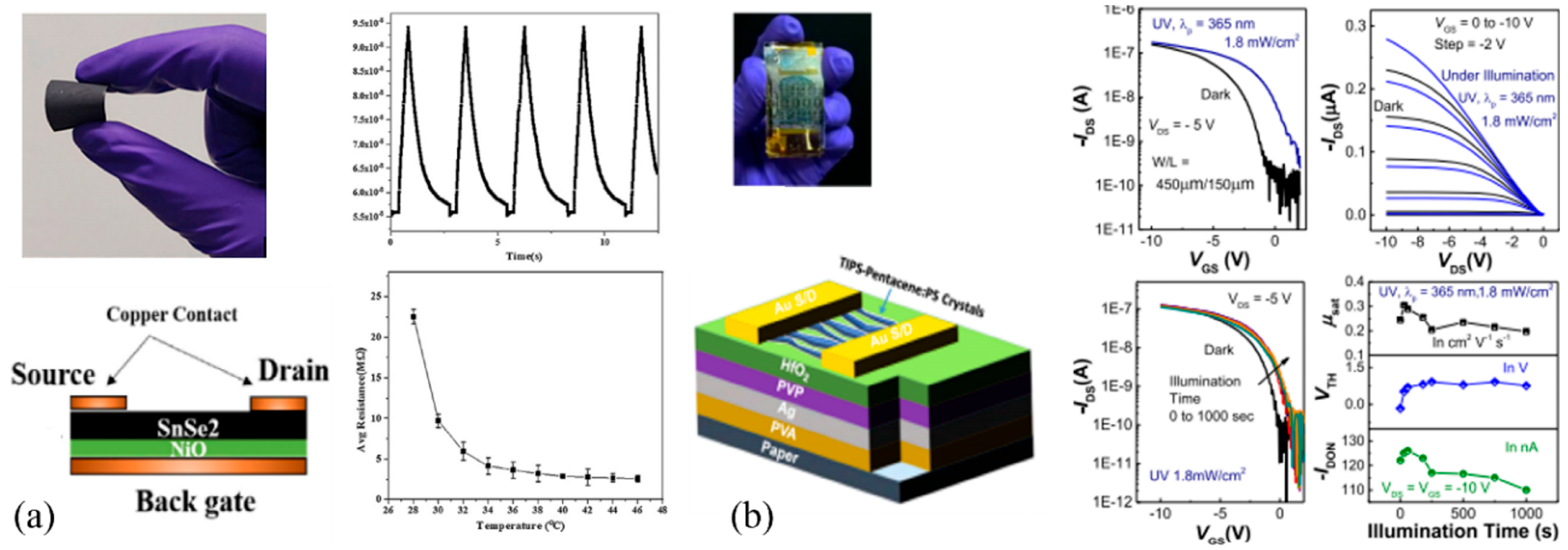
- Veeralingam, S.; Badhulika, S. 2D—SnSe2 Nanoflakes on Paper with 1D—NiO Gate Insulator Based MISFET as Multifunctional NIR Photo Switch and Flexible Temperature Sensor. Mater. Sci. Semicond. Process 2020, 105, 104738. [Google Scholar] [CrossRef]
- Raghuwanshi, V.; Bharti, D.; Mahato, A.K.; Varun, I.; Tiwari, S.P. Solution-Processed Organic Field-Effect Transistors with High Performance and Stability on Paper Substrates. ACS Appl. Mater. Interfaces 2019, 11, 8357–8364. [Google Scholar] [CrossRef] [PubMed]
- Wang, X.; Yu, C. Flexible Low-Voltage Paper Transistors Harnessing Ion Gel/Cellulose Fiber Composites. J. Mater. Res. 2020, 35, 940–948. [Google Scholar] [CrossRef]
- Kim, S.; Cook, B.; Le, T.; Cooper, J.; Lee, H.; Lakafosis, V.; Vyas, R.; Moro, R.; Bozzi, M.; Georgiadis, A.; et al. Inkjet-Printed Antennas, Sensors and Circuits on Paper Substrate. IET Microw. Antennas Propag. 2013, 7, 858–868. [Google Scholar] [CrossRef]
- Mitra, K.Y.; Polomoshnov, M.; Martínez-Domingo, C.; Mitra, D.; Ramon, E.; Baumann, R.R. Fully Inkjet-Printed Thin-Film Transistor Array Manufactured on Paper Substrate for Cheap Electronic Applications. Adv. Electron. Mater. 2017, 3, 1700275. [Google Scholar] [CrossRef]
- Kamali-Sarvestani, R.; Martin, B.; Brayden, L. Design and Fabrication of Ink-Jet Printed Logic Gates Using SWCNT-FET for Flexible Circuit Applications. In Proceedings of the 2019 IEEE International Symposium on Circuits and Systems (ISCAS), Sapporo, Japan, 26–29 May 2019; pp. 1–5. [Google Scholar]
- Wang, X.; Gao, Y.; Liu, Z.; Luo, J.; Wan, Q. Flexible Low-Voltage IGZO Thin-Film Transistors With Polymer Electret Gate Dielectrics on Paper Substrates. IEEE Electron. Device Lett. 2019, 40, 224–227. [Google Scholar] [CrossRef]
- Raghuwanshi, V.; Bharti, D.; Mahato, A.K.; Varun, I.; Tiwari, S.P. TIPS-Pentacene:PS Blend Organic Field-Effect Transistors with Hybrid Gate Dielectric on Paper Substrate. In Proceedings of the 2019 International Symposium on VLSI Technology, Systems and Application (VLSI-TSA), Hsinchu, Taiwan, 22–25 April 2019; pp. 1–5. [Google Scholar]
- Pettersson, F.; Remonen, T.; Adekanye, D.; Zhang, Y.; Wilén, C.-E.; Österbacka, R. Environmentally Friendly Transistors and Circuits on Paper. ChemPhysChem 2015, 16, 1286–1294. [Google Scholar] [CrossRef]
- Shao, F.; Feng, P.; Wan, C.; Wan, X.; Yang, Y.; Shi, Y.; Wan, Q. Multifunctional Logic Demonstrated in a Flexible Multigate Oxide-Based Electric-Double-Layer Transistor on Paper Substrate. Adv. Electron. Mater. 2017, 3, 1600509. [Google Scholar] [CrossRef]
- Martins, R.; Gaspar, D.; Mendes, M.J.; Pereira, L.; Martins, J.; Bahubalindruni, P.; Barquinha, P.; Fortunato, E. Papertronics: Multigate Paper Transistor for Multifunction Applications. Appl. Mater. Today 2018, 12, 402–414. [Google Scholar] [CrossRef]
- Liu, Z.; Nie, S.; Luo, J.; Gao, Y.; Wang, X.; Wan, Q. Flexible Indium-Tin-Oxide Homojunction Thin-Film Transistors with Two In-Plane Gates on Cellulose-Nanofiber-Soaked Papers. Adv. Electron. Mater. 2019, 5, 1900235. [Google Scholar] [CrossRef]
- Nie, S.; Wang, X.; Liu, R.; Jiang, S.; Yang, X.; Wan, Q. Flexible ITO-Based TFTs on Paper Substrates. In Proceedings of the 2018 9th Inthernational Conference on Computer Aided Design for Thin-Film Transistors (CAD-TFT), Shenzhen, China, 16–18 November 2018; p. 23. [Google Scholar]
- Dou, W.; Tan, Y. Junctionless Dual In-Plane-Gate Thin-Film Transistors with AND Logic Function on Paper Substrates. ACS Omega 2019, 4, 21417–21420. [Google Scholar] [CrossRef]
- Guo, L.; Xu, G.; Xu, C.; Cheng, G.; Ding, J. Egg Albumen-Based Biopolymer Electrolyte Lateral Capacitive Coupling Thin-Film Transistors on Logical Operation. Org. Electron. 2021, 93, 106109. [Google Scholar] [CrossRef]
- Han, S.-T.; Zhou, Y.; Roy, V.a.L. Towards the Development of Flexible Non-Volatile Memories. Adv. Mater. 2013, 25, 5425–5449. [Google Scholar] [CrossRef] [PubMed]
- Ni, Y.; Wang, Y.; Xu, W. Recent Process of Flexible Transistor-Structured Memory. Small 2021, 17, 1905332. [Google Scholar] [CrossRef] [PubMed]
- Shih, C.-C.; Lee, W.-Y.; Chen, W.-C. Nanostructured Materials for Non-Volatile Organic Transistor Memory Applications. Mater. Horiz. 2016, 3, 294–308. [Google Scholar] [CrossRef]
- Xu, M.; Zhang, X.; Li, S.; Xu, T.; Xie, W.; Wang, W. Gate-Controlled Multi-Bit Nonvolatile Ferroelectric Organic Transistor Memory on Paper Substrates. J. Mater. Chem. C 2019, 7, 13477–13485. [Google Scholar] [CrossRef]
- Kim, M.G.; Han, D.H.; Kim, S.Y.; Lee, G.G.; Park, K.E.; Park, B.E.; Han, S.P. Fabrication of a Paper Memory Transistor by Using a Solution Process. J. Korean Phys. Soc. 2020, 76, 1088–1091. [Google Scholar] [CrossRef]


| Type | Active Materials | Substrate | Range | Fabrication Method | Ref. |
|---|---|---|---|---|---|
| Relative humidity | Carbon black, exfoliated graphene | Filter paper | 33–95% | Dip coating | [62] |
| 2B graphite, ethanol | White, non-glossy, hard cellulose | 43–83% | Hand-drawn | [63] | |
| rGO/PANI | Polypropylene filter paper (0.22 μm) | 0–98% | Filtering | [64] | |
| Graphene | Filter paper | 10–98% | LIG | [65] | |
| Nanoporous SiO2–Al2O3 | P:E smart paper, PEL P60 | 15–92% | Inkjet printing | [66] | |
| CNTs | (TEMPO)-oxidized cellulose fibers | 11–95% | Self-assembly | [67] | |
| GO, Al | – | 30–90% | Self-assembly, thermal evaporation | [68] | |
| Cellulose nanofiber/CNT | Custom PBHS with different weights | 11–95% | Roll-to-roll | [69] | |
| Writing carbon ink | A4 paper (80 g m−2) | 18–91% | Dipping, spraying | [70] | |
| EPTAC-cellulose and Ag electrodes | 11–95% | Bath, stirring, and screen printing | [71] | ||
| Ionic conductive WCN—TEMPO and Au | 7–94% | Stirring, shadow mask | [72] | ||
| MWCNTs–Ag | Porous paper (PPHS) | 10–90% | Screen printing, gravure printing | [73] | |
| Al–PI–polyester conductive adhesive tape | 41.1–91.5% | – | [74] | ||
| Bacterial cellulose—CNTs | – | 0–98% | Mayer rod | [75] | |
| Edible rice paper | 0–100% | Drawing | [76] | ||
| Pressure | GO-cellulose composite paper | 0–20 kPa | Thermal reduction | [56] | |
| Carbonized graphene-coated wastepaper aerogel | 0.3–5 kPa | Stirring, molding, annealing | [58] | ||
| rGO/PMMA porous structure/PI | 0–2.5 MPa | Vacuum filtration | [59] | ||
| Microporous, free-shaped reduced graphene oxide paper/PI | 0–60 kPa | Evaporation-induced self-assembly | [60] | ||
| Graphene/ZnO | Paper, cotton | 0–100 kPa | Coating, in situ synthesis | [45] | |
| CNT | Printing paper | – | Elevated temperature pressing | [77] | |
| CNT/PI | Paper | 8–140 kPa | Spray coating | [78] | |
| CNT/PDMS/PI | Tissue paper | 0–42 kPa | Handwriting | [79] | |
| Chitosan/potato starch/PVA/FeCl3 | 0–250 kPa | Molding | [80] | ||
| Strain | Carbonized graphene-coated wastepaper aerogel | 0–75% | Stirring, molding, annealing | [58] | |
| rGO/PMMA porous structure/PI | 0–10% | Vacuum filtration | [59] | ||
| Microporous, free-shaped reduced graphene oxide paper/PI | 7.6–11% | Evaporation-induced self-assembly | [60] | ||
| Graphene | Mulberry paper | 0.28–0.58% | Meyer-rod coating | [61] | |
| MWCNT/PDMS | Photo paper | 0–130° | Screen printing | [81] | |
| CNT/poly-m-phenylene isophthalamide (PMIA) | – | Hot-press | [82] | ||
| MWCNT/PET | Paper | 0–1.72% | Screen printing/lamination | [83] | |
| Graphene | Nanocellulose-based | 0.55% | Scrape coating/deep coating | [84] | |
| CB/Graphene/SiO2 | Sodium carboxymethyl | −1.0–1.0% | Dip coating | [85] | |
| Chitosan/Potato starch/PVA/FeCl3 | 200% | Molding | [80] | ||
| Active Materials | Principle | Target Analyte | LoD * | Ref. |
|---|---|---|---|---|
| Graphene-PEDOT/PSS, WS2 | Electrical | Butanol | 50 ppm | [88] |
| Gold, nanostructured latex-coated paper | Electrical, colorimetric | H2S | 1.5 ppm | [89] |
| Carbon black | Electrical | Bisphenol A | 0.03 μM | [90] |
| CdTe and ZnCdSe quantum dots—nanoporphyrins | Colorimetric | Organophosphorus (dimethoate) | 1 μgL−1 | [94] |
| Perovskite halide CH3NH3PbI3 (MAPI) | Electrical | NH3 | <1 ppm | [95] |
| Graphene paper, Nafion, Bi nanoparticles | Electrical | Pb2+, Cd2+ | 0.1 ppb | [96] |
| GO, ZnO nanoparticles, EDTA | Electrical | Cd2+, Pb2+, Cu2+, Hg2+ | 1–6.8 μM | [97] |
| AgNPs | Colorimetric | Hg2+ | 10 µgL−1 | [98] |
| Citrate capped Cu@Ag core–shell nanoparticles | Colorimetric | Phenthoate | 50–200 μgL−1 | [46] |
| γ-MnOOH nanowires | Colorimetric | Organophosphorus (AChE, omethoate) | 0.1 mU mL−1, 10 ng mL−1 | [100] |
| Quantum carbon dots, CdZnTe quantum dots | Fluorescence | Hg2+-Sulfide | 0.002 and 1.488 μM | [101] |
| Belt-like ZnSe nanoframes | Colorimetric | Ag+, Cu2+, Hg2+ | 5 ppm, 1 ppm | [102] |
| Au@Ag NPs | Colorimetric | TNT | 0.35 μg/mL | [103] |
| Colloidal gold labeled mice monoclonal antibody | Colorimetric | Toltrazuril | <2.60 μg/kg | [104] |
| Active Materials | Range | LoD * (μΜ) | Output | Fabrication Method | Ref. |
|---|---|---|---|---|---|
| Graphene/Cu2O | 0.5–5166 μM | 0.21 | Electrical | CVD-thermal decomposition | [115] |
| Graphene/PtCo alloy NPs | 0.035–30 μM | 5 | Electrical | Electrochemical deposition | [116] |
| Graphene/CuO/Cu(OH)2 | 50 μM–10 mM | 7 | Electrical | Thermal-laser modification | [117] |
| rGO/Cu nanoflower | 2 μM–13 mM | 0.5 | Electrical | Mold casting–electrochemical deposition | [118] |
| AuNPs/graphene paper | 15 μM–8 mM | 2.5 | Electrical | Sputtering and thermal, laser dewetting | [119] |
| Carbon, cobalt phthalocyanine, graphene, ionic liquid | 0.01–5.0 mM | 0.67 | Electrical | Wax printing, screen printing, drop casting | [120] |
| Aniline functionalized graphene quantum dots, PBA | 0.05–20 mM | 2.1 | Optical | Inkjet, drop casting | [121] |
| Graphene nanosheets, carbon nanotubes, PtAu | 0.1–11.6 mM | 8.0 | Electrical | Roll printing, electrodeposition | [123] |
| Activated carbon, Cu(II) | 0.0004–7 mM | 0.2 | Electrical | Drop cast | [124] |
| Graphite powder, Cu(II) | 0.00007–5 mM | 0.05 | Electrical | Drop cast | [124] |
| MWCNT-COOH, Cu(II) | 0.00002–8 mM | 0.02 | Electrical | Drop cast | [124] |
| Cu(II)/MWCNT-COOH (1:5) | 0.0003–9 mM | 0.3 | Electrical | Drop cast | [124] |
| rGO-TEPA/PB | 0.1–25 mM | 25 | Electrical | Screen printing, photolithography | [126] |
| Prussian blue–graphene modified with GOx and chitosan | 2–650 μM | – | Electrical | Wet spinning | [127] |
| Chitosan/GOx/horseradish peroxidase/TMB | 0–250 μM | 10 | Optical | Wax soaking, drop cast | [136] |
| Fluorescent silicon nanodots/graphene | 2.68–200 μM | – | Fluorescence | Laser engraving, LIG | [137] |
| Graphite/Ag/AgCl/graphene-COOH | 5–500 pM | 0.0015 | Capacitive | Hand-drawing, drop cast | [138] |
| AuNP–AgNP | 500–6.000 μM | 340.0 | Optical | Wax printing, drop cast | [135] |
| Ni–HHTP | – | 1.30 | Electrical | Screen printing, drop cast | [139] |
| Ion/Ioff | Carier Mobility (cm2V−1S−1) | Threshold Voltage (VTH) (V) | Semiconductor | Dielectric | Type of Device | Applications | Ref. |
|---|---|---|---|---|---|---|---|
| ~103–104 | 0.97 | 0.67 | Poly(3-hexylthiophene) (P3HT) | Ion-gel dielectric | OFETs | Sensing applications | [181] |
| ~106 | ~3 | - | Single-walled carbon nanotubes (SWCNTs) | Aluminum oxide (Al2O3) | TFTs | Sensing applications—smart packaging, attachable displays | [182] |
| 2.8(±0.9) × 103 | 0.14 ± 0.05 | 1.04 ± 0.15 | Poly(3-hexylthiophene) (P3HT) | Ion-gel dielectric | OTFTs | Sensing applications—foldable electronics | [183] |
| 7.6 × 10⁶ | 14.6 | 0.46 | Indium zinc oxide (IZO) | Organic beeswax | TFTs | Sensing applications—portable electronics (Human body related sensors) | [184] |
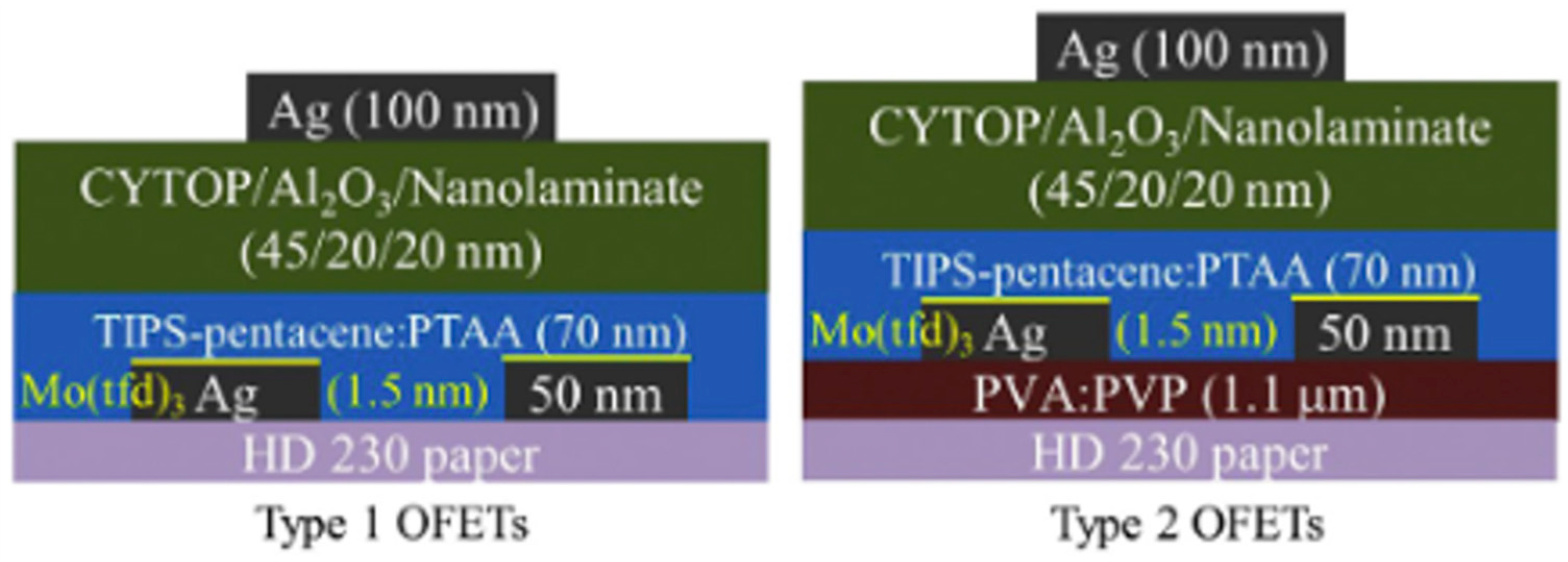
| ~105 | 1.7 ± 1.1 10−1 | 1.4 ± 0.2 | 6,13-Bis(triisopropylsilylethynyl) pentacene (TIPS-pentacene) and Poly[bis(4- phenyl)(2,4,6-trimethylphenyl)amine] (PTAA) (1:1 wt%) | CYTOP/Aluminum oxide (Al2O3)/nanolaminate (NL) | OFETs | Sensing applications | [180] |
| ~103 | 6.2 (p-type), 2 (n-type) | 7.3 (p-type), 7.8 (n-type) | Polycrystalline silicon (poly-Si) | Silicon dioxide (SiO2) | TFTs | Sensing applications—smart packages, biodegradable health monitoring units, flexible displays, and disposable sensor nodes | [175] |
| 1.7 × 10⁶ | 218.3 | - | Indium oxide (In2O3) nanowires | Microporous silicon dioxide (M-SiO2) | NW-PFETs | Sensing applications—battery-powered-portable sensors | [185] |
| >109 | ~6 | - | Graphene/molybdenum disulfide (MoS2) | Aluminum oxide (Al2O3) | Monolayer GFETs | Sensing applications—disposable smart wireless nanosystems and sensors | [188] |
| >107 | 0.25 ± 0.023 | 35.73 ± 1.28 | Dinaphthothienothiophene (DNTT) | CYTOP | OFETs | Sensing applications | [189] |
| >103 | 0.07 | - | Zinc oxide (ZnO) | Polymer electrolyte | EGTs | Sensing applications—biosensors, smart packaging, wearable electronics | [190] |
| 46 | - | - | PEDOT/PSS | Cellulose-based electrolyte sticker | OECTs | Sensing applications | [191] |
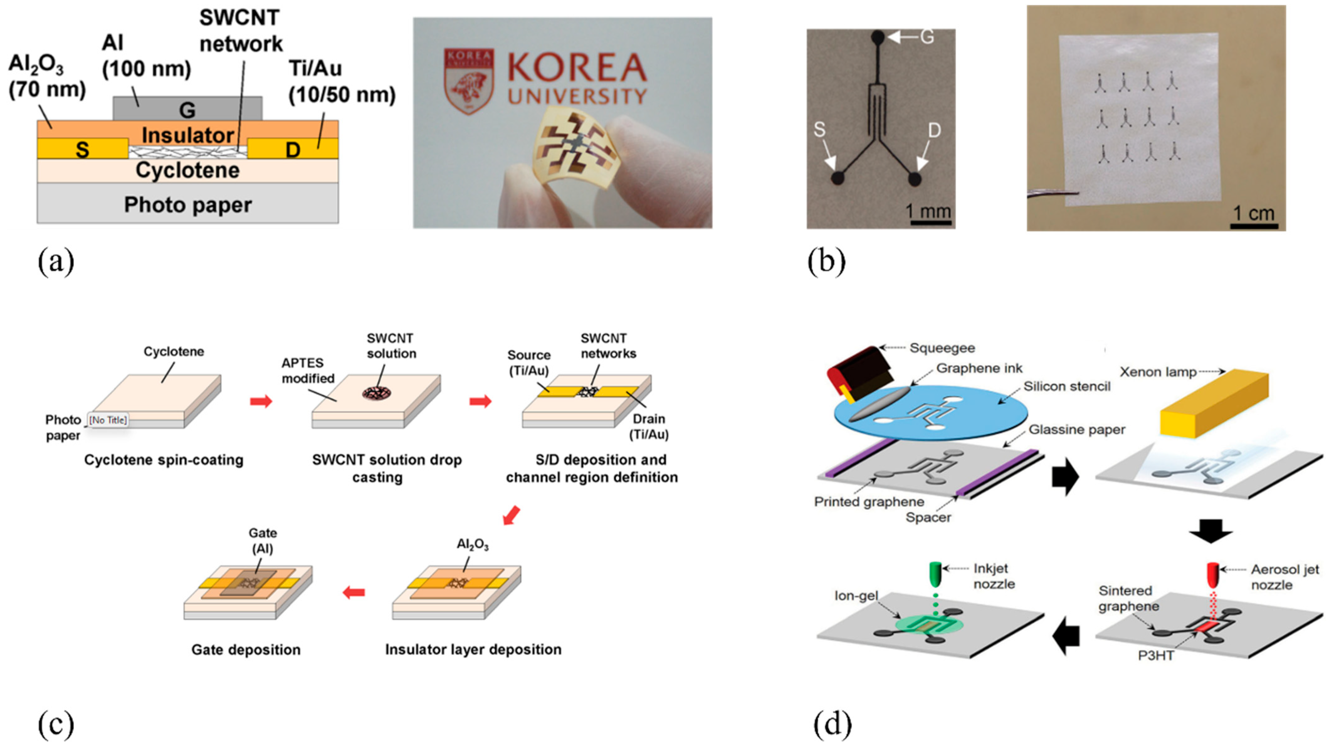
| - | - | - | Graphene | Solution-soaked paper | GFETs | Biosensors—glucose and ssDNA sensors | [192] |
| - | - | - | Hybrid FET device—Commercial Si-based MOSFET (MC14007UBCP) on cellulose paper | EGFETs | Biosensors—pH sensors | [170] | |
| 102 | 20 | - | Tin selenide (SnSe2) | Nickel oxide (NiO) | MISFETs | Temperature–photo switch sensors | [193] |
| ~105 | 0.22 ± 0.11 (Average)/0.44 (Maximum) | 0.021± 0.63 | TIPS-pentacene: polystyrene blend | Poly(4-vinylphenol)/HfO2 | OFETs | Optical light sensors | [194] |
| - | - | - | Pencil graphite | Cellulose filter paper | Carbon-based PFETs | Strain sensors (human motion detection) | [173] |
| 99 | 18.7 | - | Graphene/molybdenum disulfide (Gr/MoS2) | Cellulose paper | Gr/MoS2 PFETs | Strain sensors (human motion detection) | [172] |
| >104 | 9.1 | 1.8 | Indium gallium zinc oxide (IGZO) | Ion-gel/cellulose fiber composite dielectric | TFTs | Tactile sensors; digital circuits—inverter, multiplexed active-matrix arrays | [195] |
| Ion/Ioff | Carier Mobility (cm2V−1S−1) | Threshold Voltage (VTH) (V) | Semiconductor | Dielectric | Type of Device | Applications | Ref. |
|---|---|---|---|---|---|---|---|
| 200 ± 130 | 0.086 ± 0.003 | 0.7 ± 0.1 | FS-0027 organic semiconductor ink (PTAA (Poly(3-hexylthiophene-2,5-diyl))-based) | Amorphous silica–MMAcoMAA | TFTs | Digital circuits | [197] |
| - | - | - | Single-walled carbon nanotubes (SWCNTs) | Poly(methyl methacrylate) (PMMA) | SWCNT FET | Digital circuits—logic gates | [198] |
| 104 | 21.7 ± 2.70 | - | Zinc oxide (ZnO)/carboxymethyl cellulose (CMC) | Cellulose-based ionic conductive hydrogel (CICH) sticker | EGTs | Digital circuits—logic gates | [47] |
| 1.8 × 10⁷ | 42 | 0.79 | Indium gallium zinc oxide (IGZO) | Graphene oxide-enhanced poly(vinyl alcohol) (PVA) | TFTs | Digital circuits—resistor loaded inverter | [199] |
| ~104 | 0.56(±0.16) | 0.56(±0.24) | TIPS-pentacene/polystyrene blend | Bilayer dielectric (HfO2/PVA) | OFETs | Digital circuits—resistor loaded inverter | [200] |
| 7200 | 2.6 × 10⁻³ | 0.6 | Poly(3-hexylthiophene) (P3HT) blended with Poly(L-lactic acid) (PLLA) (20:80 wt%) | Deep eutectic mixture of sorbitol + choline chloride (CSorb) solidified with a commercial water-based binder | IMTs | Digital circuits—logic gates, inverters, ring oscillators and memories | [201] |
| 107 (p-type), 4 × 10⁶ (n-type) | 1.12 (p-type), 0.17 (n-type) | 1.4 (p-type) | Dinaphtho[2,3-b:2′,3′-f]thieno[3,2-b]thiophene (DNTT) (p-type)/ Polyera ActivInk N1100 (PTCDI derivative) (n-type) | Aluminum oxide and alkyl or fluoroalkylphosphonic acid self-assembled monolayer (SAM) | TFTs | Digital circuits—unipolar and complementary ring oscillators | [48] |
| >107 | 26 | ~0.52 | Indium zinc oxide (IZO) | Cellulose nanofiber (CNF) electrolyte with EDL capacitance | EDL-TFTs | Digital circuits—inverters, logic gates | [202] |
| >104 | ~2 | - | Indium gallium zinc oxide (IGZO) | Paper (cellulose-based) | MISFETs | Digital circuits—logic gates | [203] |
| 7.5 × 10⁶ | 7.8 | 0.32 | Indium tin oxide (ITO) | Cellulose nanofiber (CNF)-soaked paper | TFTs | Digital circuits—logic gates, inverters | [204] |
| - | - | - | Indium tin oxide (ITO) | Ionic liquid (1-ethyl-3-methylimidazolium tetrafluoroborate) + chitosan on paper | TFTs | Digital circuits—logic gates, inverters | [205] |
| 5.8 × 10⁶ | 12.8 | −0.53 V to 0.97 V (via secondary gate) | Indium tin oxide (ITO) | Chitosan (solution-processed) | TFTs | Digital circuits—logic gates | [206] |
| ~10⁶ | ~12.8 | ~0.1 | Indium tin oxide (ITO) | Egg albumen-based biopolymer electrolyte | TFTs | Digital circuits—logic gates, inverters | [207] |
| ~1.1 × 10⁶ | ~11.5 | 2.5 | Indium gallium zinc oxide (IGZO) | Chicken albumen, enhanced with Al2O3 | TFTs | Transistor memories | [49] |
| - | ~0.92 cm2/V·s (max); ~0.71 cm2/V·s (average) | - | Pentacene | Cross-linked PVP P(VDF-TrFE-CTFE) AlOx/PMMA | OFETs | Transistor memories | [211] |
| ~3.45 × 10² | - | - | P3HT (poly(3-hexylthiophene)) | P(VDF-TrFE) | FeFETs | Transistor memories | [212] |
| Technique | Principle | Output | Sensing Application Examples |
|---|---|---|---|
| Resistive/capacitive | Change in impedance upon stimulus | Electrical | Humidity [65], pressure [59], strain [83] |
| Electrochemical | Redox signal at printed electrodes | Electrical | Glucose [123], VOCs [62] |
| FET-based sensing | Current modulation via gate-channel field | Electrical | Glucose [192], nucleic acid detection [185] |
| Colorimetric | Color change by reaction | Optical | Heavy metals [99], pesticides [53] |
| Fluorescence | Light emission under excitation | Optical | Cancer [145], health [93] biomarkers |
| Device Type | Functionality | Complexity | Fabrication Techniques | Materials Used | Advantages | Limitations |
|---|---|---|---|---|---|---|
| Resistive/Capacitive Sensors | Detect humidity, pressure, strain, temperature | Low | Dip-coating, laser patterning, hand-drawing | Graphene, CNTs, graphite, rGO, cellulose composites | Simple, low-cost, flexible, disposable | Limited sensitivity and selectivity; environmental instability |
| Optical Sensors | Colorimetric or fluorescence detection of analytes | Medium | Drop casting, printing, nanoparticle deposition | AgNPs, CuNPs, QDs, graphene oxide, dyes | Visual readout, smartphone-compatible, user-friendly | Limited quantification; often single use; dependent on lighting |
| Electrochemical Sensors | Measure redox reactions for analyte detection | Medium–High | Screen printing, inkjet printing, electrode modification | Carbon inks, metal oxides, conductive polymers | High sensitivity, quantitative, scalable | Requires external reader; sensitive to interference and drift |
| PFETs (Field-Effect Transistors) | Signal amplification, switching, sensing, logic | High | Printing, vapor deposition, doping, photolithography | Organic semiconductors, ion gels, graphene, PEDOT/PSS | Enable active electronics, logic gates, multifunctionality | Poor mobility/stability; complex fabrication; low integration maturity |
Disclaimer/Publisher’s Note: The statements, opinions and data contained in all publications are solely those of the individual author(s) and contributor(s) and not of MDPI and/or the editor(s). MDPI and/or the editor(s) disclaim responsibility for any injury to people or property resulting from any ideas, methods, instructions or products referred to in the content. |
© 2025 by the authors. Licensee MDPI, Basel, Switzerland. This article is an open access article distributed under the terms and conditions of the Creative Commons Attribution (CC BY) license (https://creativecommons.org/licenses/by/4.0/).
Share and Cite
Barmpakos, D.; Apostolakis, A.; Jaber, F.; Aidinis, K.; Kaltsas, G. Recent Advances in Paper-Based Electronics: Emphasis on Field-Effect Transistors and Sensors. Biosensors 2025, 15, 324. https://doi.org/10.3390/bios15050324
Barmpakos D, Apostolakis A, Jaber F, Aidinis K, Kaltsas G. Recent Advances in Paper-Based Electronics: Emphasis on Field-Effect Transistors and Sensors. Biosensors. 2025; 15(5):324. https://doi.org/10.3390/bios15050324
Chicago/Turabian StyleBarmpakos, Dimitris, Apostolos Apostolakis, Fadi Jaber, Konstantinos Aidinis, and Grigoris Kaltsas. 2025. "Recent Advances in Paper-Based Electronics: Emphasis on Field-Effect Transistors and Sensors" Biosensors 15, no. 5: 324. https://doi.org/10.3390/bios15050324
APA StyleBarmpakos, D., Apostolakis, A., Jaber, F., Aidinis, K., & Kaltsas, G. (2025). Recent Advances in Paper-Based Electronics: Emphasis on Field-Effect Transistors and Sensors. Biosensors, 15(5), 324. https://doi.org/10.3390/bios15050324