High-Accuracy Characterization of a Single Thin Film on a Substrate from One Transmittance Spectrum by an Advanced Envelope Method Addressing Voids, Tail Electron Transitions, and Deep-Level Electron Transitions in a-Si Films

 , , ,
, , ,  ,
,  and
and 
Abstract
1. Introduction
2. Materials and Methods
3. Results
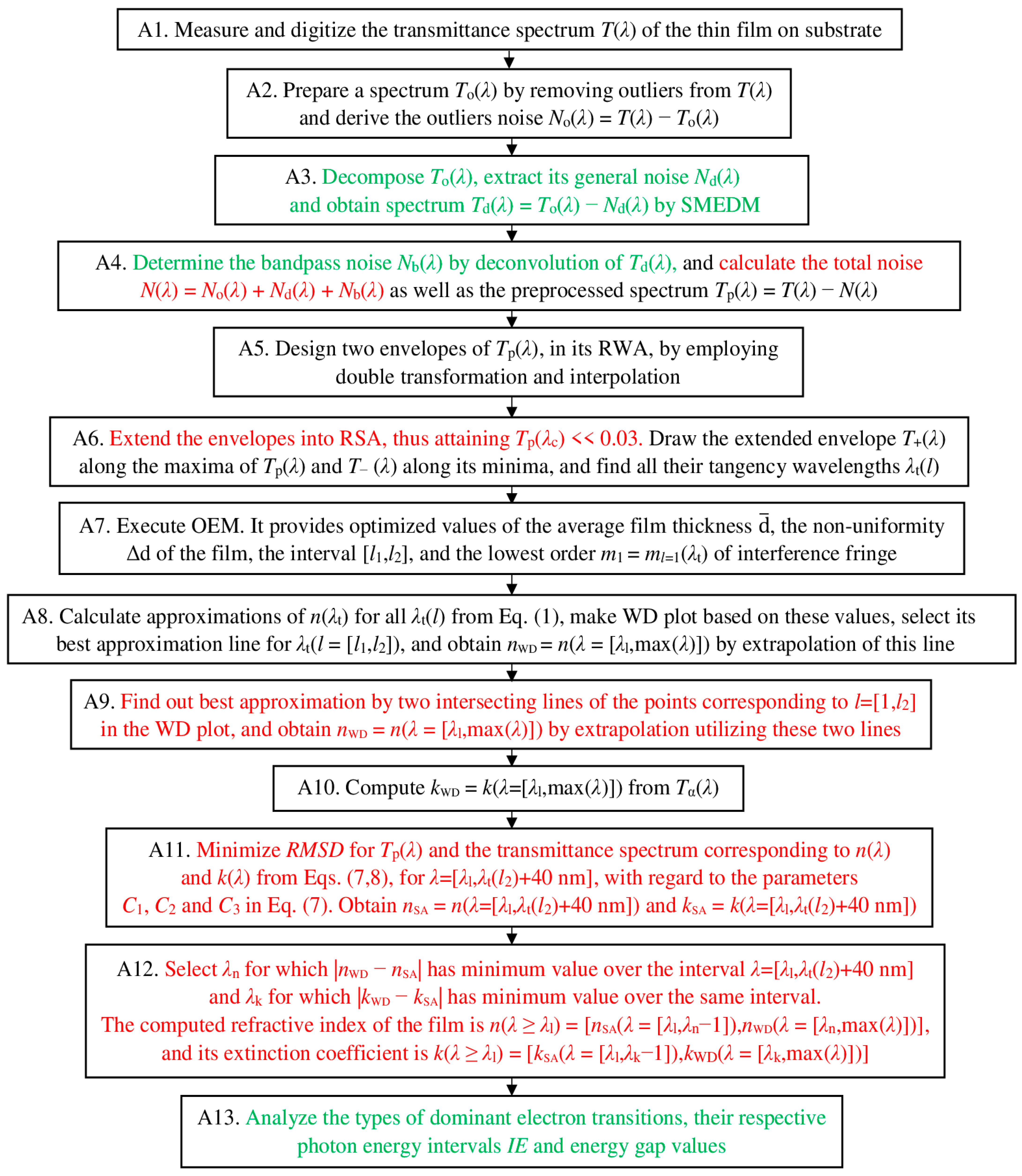
3.1. Theory and Algorithm of the Proposed Advanced Envelope Method (AEM)
3.2. Experimental Features
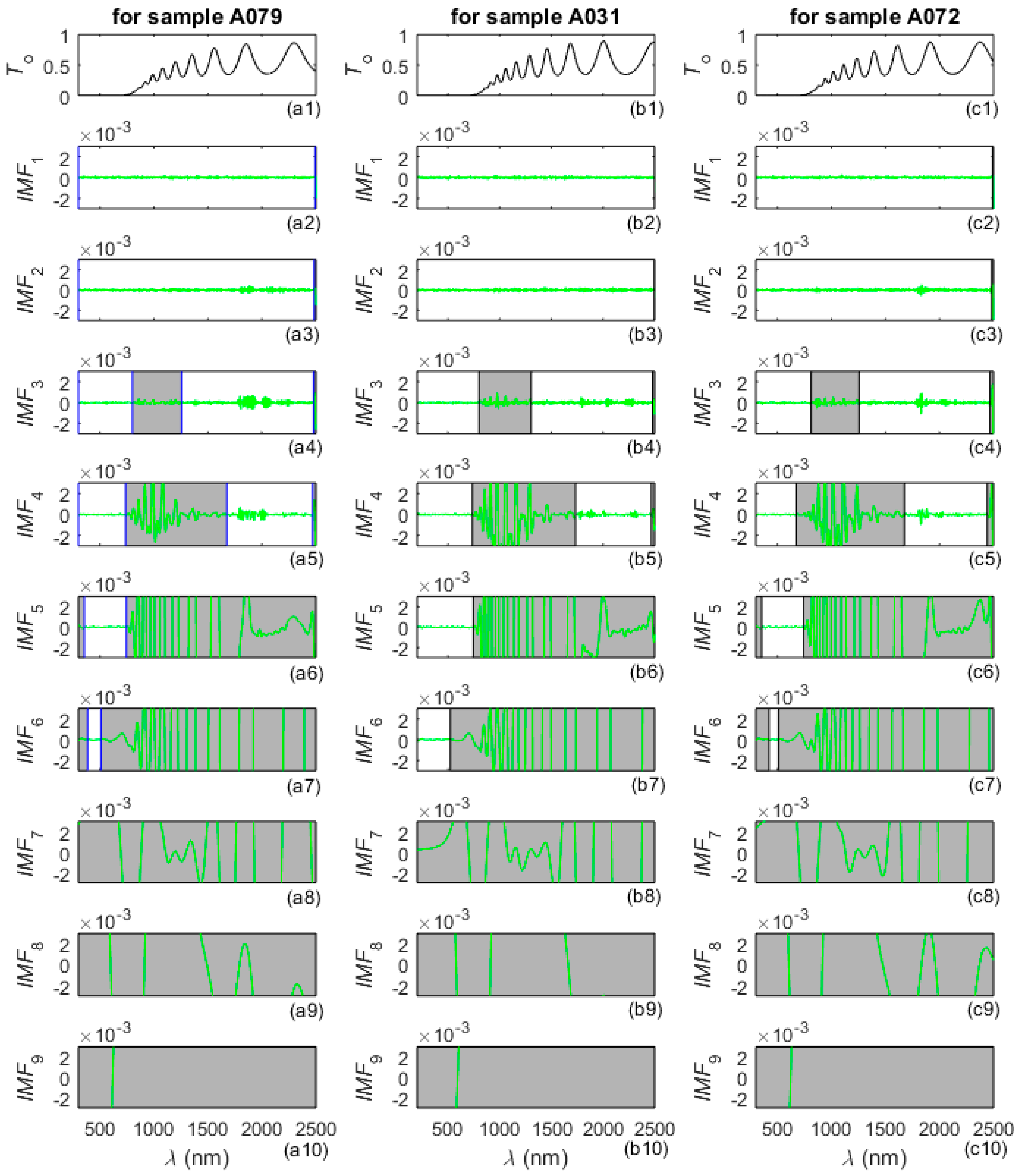
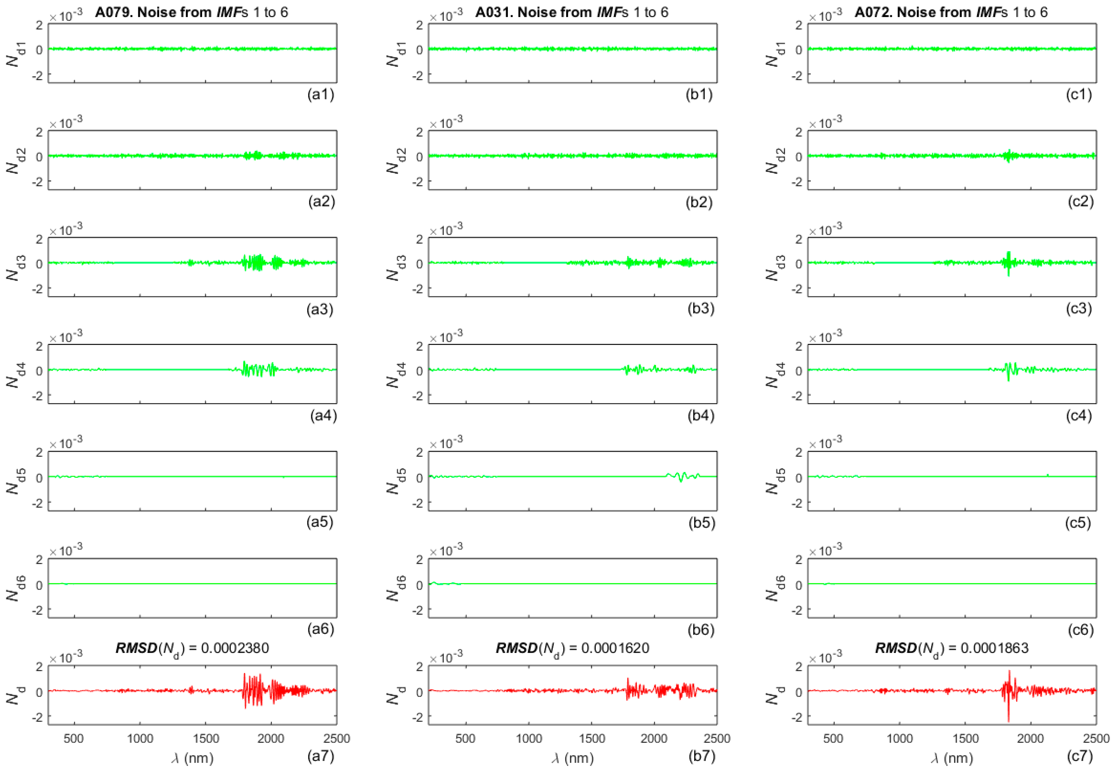
3.3. Preprocessing of the Transmittance Spectra T(λ)

3.4. Computation of Extended Envelopes and Non-Dispersion Parameters of the Spectra and the Films


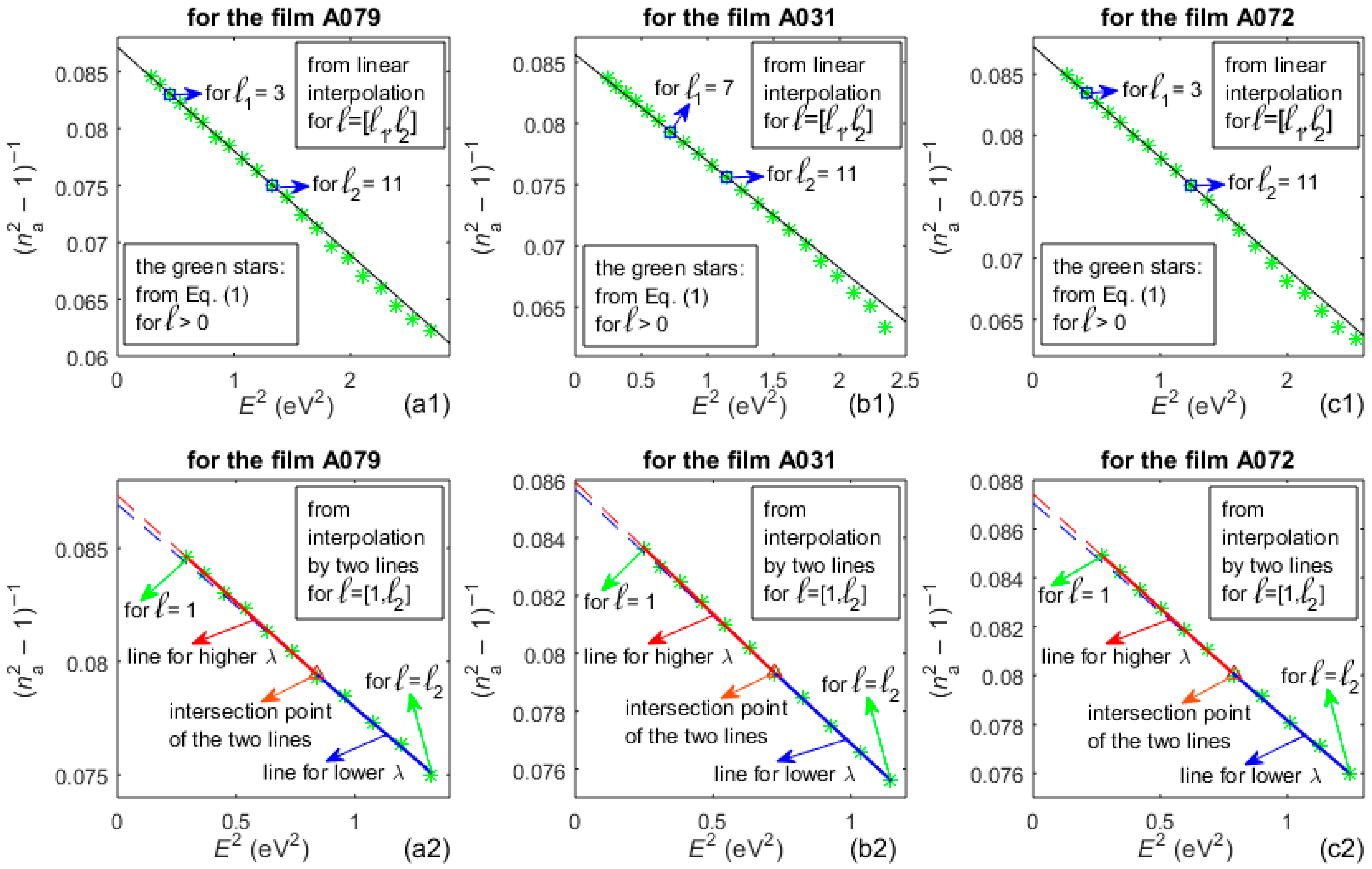
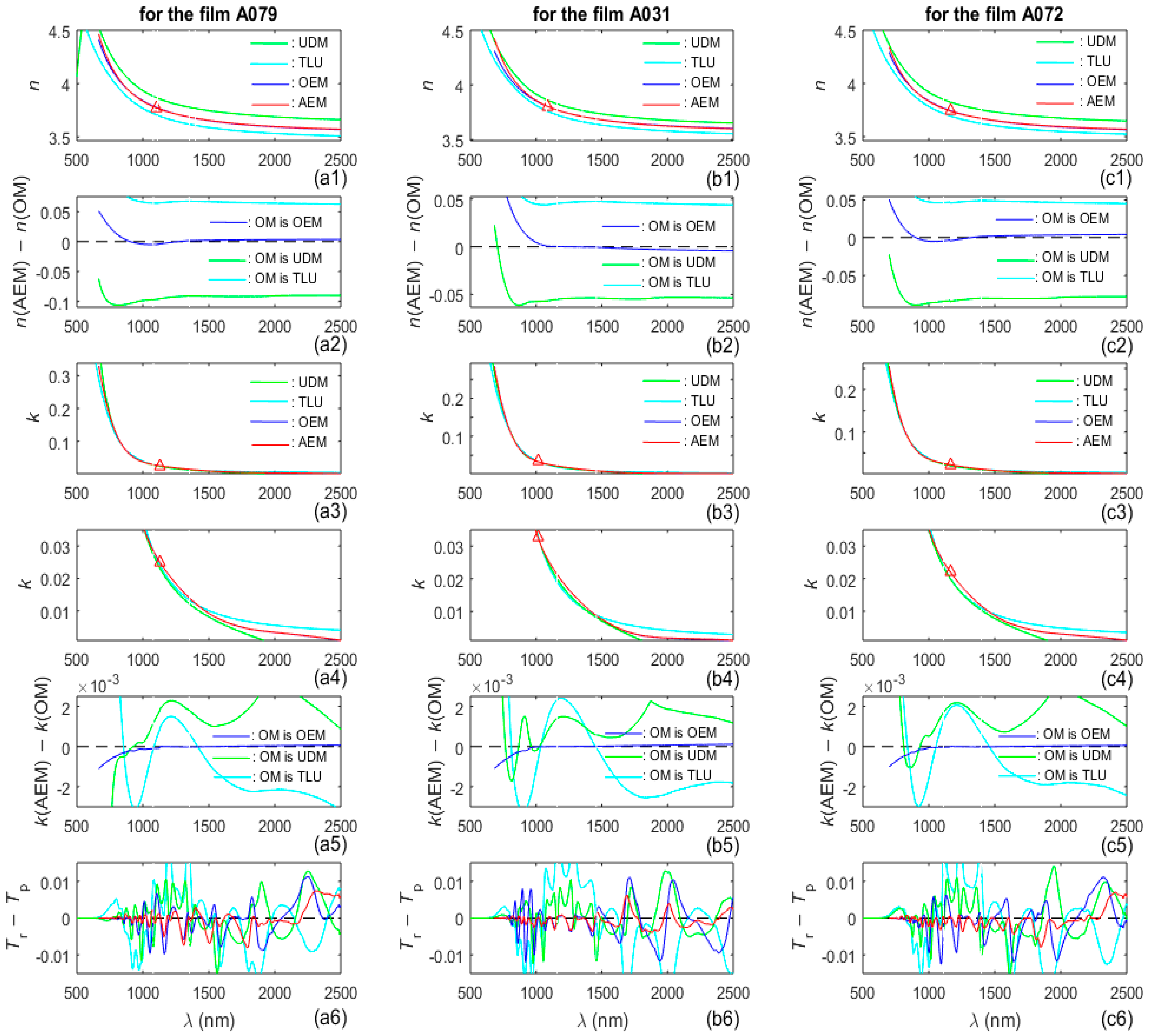
3.5. Results Regarding n(λ), k(λ), and fvoids



| Film | (nm), Δd (nm); Source | RE () (%); Source | Method | FOM [λl,λ(l2)] | FOM [λ(l2),λ(l1)] | FOM [λ > λ(l1)] | FOM [λl,max(λ)] |
|---|---|---|---|---|---|---|---|
| A079 | 1299, 0; EM from [54] | 0.850; EM from [54] | OEM | 2.80 | 4.23 | 4.56 | 4.20 |
| AEM | 0.82 | 2.90 | 3.84 | 3.30 | |||
| 1282.6, 20.0; AEM | 0.0652; AEM | TLU | 7.16 | 13.0 | 7.15 | 8.32 | |
| UDM | 3.19 | 6.37 | 6.00 | 5.60 | |||
| A031 | 1359, 0; EM from [54] | 0.662; EM from [54] | OEM | 3.86 | 2.01 | 6.09 | 5.08 |
| AEM | 1.09 | 1.59 | 2.33 | 1.96 | |||
| 1382.9, 0; AEM | 0.1028; AEM | TLU | 8.81 | 15.4 | 10.2 | 10.9 | |
| UDM | 3.89 | 4.82 | 5.43 | 4.97 | |||
| A072 | 1310, 0; EM from [54] | 0.992; EM from [54] | OEM | 3.89 | 3.51 | 5.64 | 4.99 |
| AEM | 1.10 | 1.74 | 3.23 | 2.68 | |||
| 1329.5, 8.6; AEM | 0.0504; AEM | TLU | 6.94 | 14.5 | 8.21 | 9.25 | |
| UDM | 3.53 | 6.25 | 6.21 | 5.72 |
| Film | E0 | Ed | n0 | fvoid (%) |
|---|---|---|---|---|
| A079 | 3.04 | 34.9 | 3.53 | 6.68 |
| A031 | 3.07 | 35.7 | 3.56 | 5.65 |
| A072 | 3.06 | 35.0 | 3.53 | 6.75 |
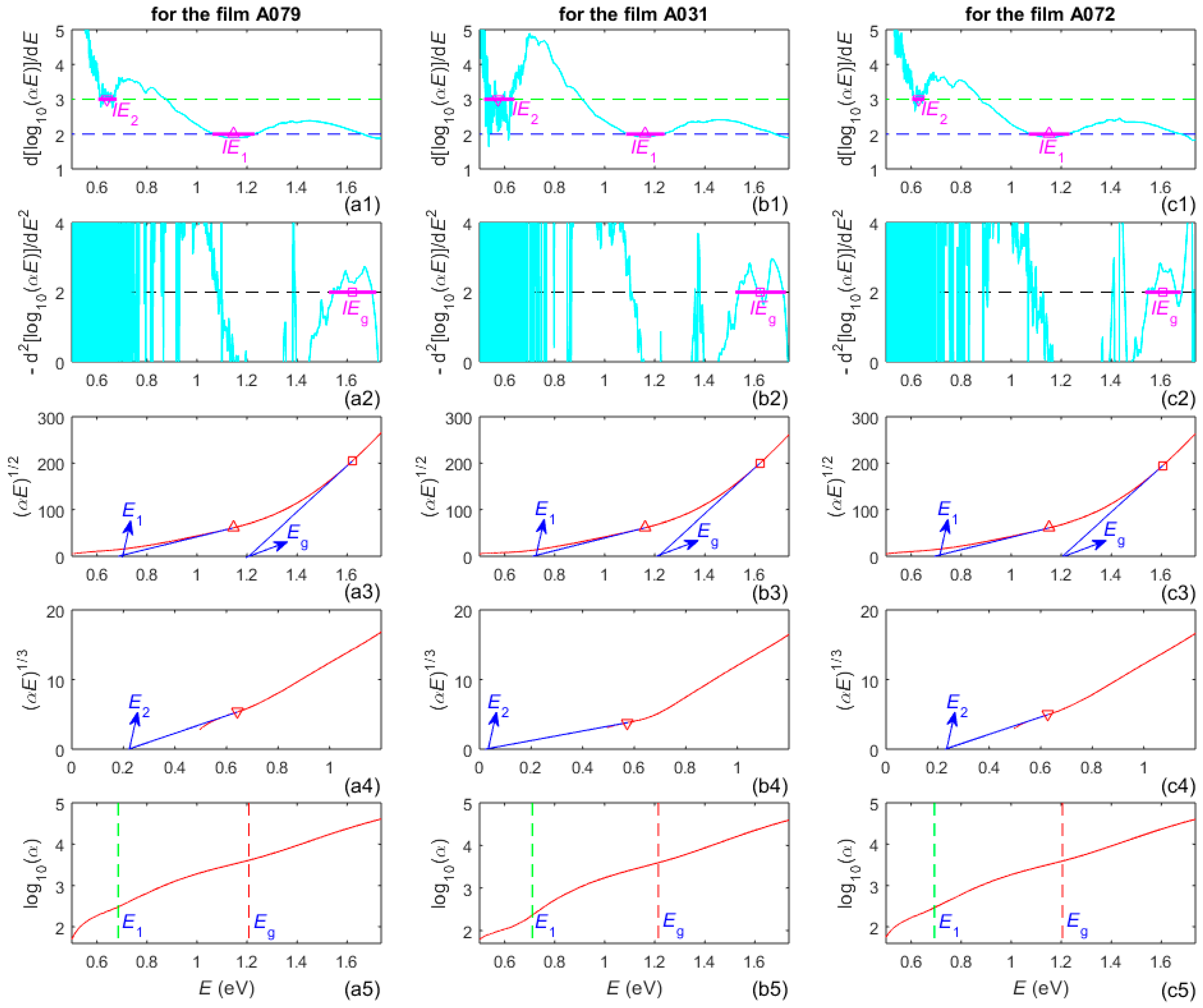
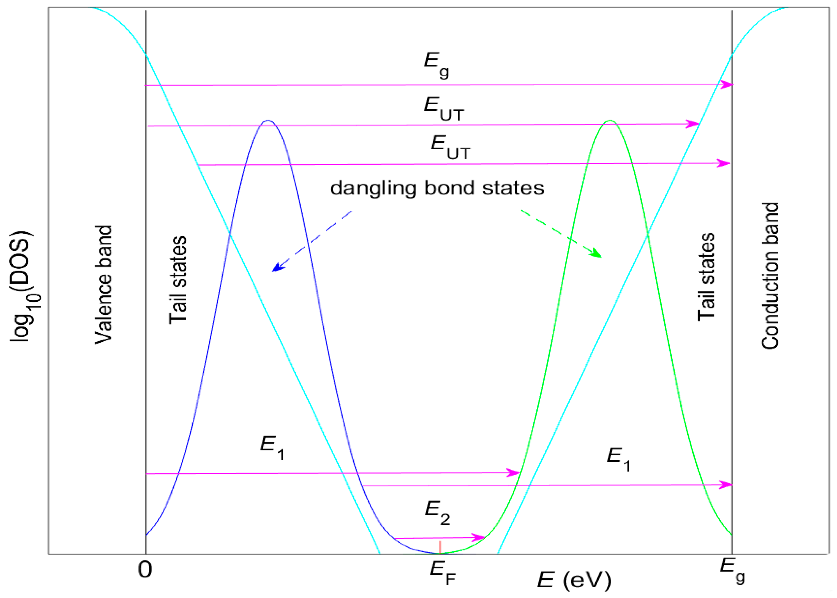
3.6. Results Related to k(λ) Computed by AEM

| Film | q | IE2 (eV) | E2 (eV) | q | IE1 (eV) | E1 (eV) | q | IEg (eV) | Eg (eV) from Figure 7 | Eg (eV) from [54] |
|---|---|---|---|---|---|---|---|---|---|---|
| A079 | 3 | [0.612,0.672] | 0.219 | 2 | [1.07,1.22] | 0.685 | 2 | [1.53,1.71] | 1.21 | 1.23 |
| A031 | 3 | [0.525,0.632] | 0.021 | 2 | [1.09,1.23] | 0.716 | 2 | [1.53,1.72] | 1.21 | 1.24 |
| A072 | 3 | [0.611,0.647] | 0.229 | 2 | [1.08,1.23] | 0.693 | 2 | [1.54,1.67] | 1.21 | 1.24 |
4. Discussion
5. Conclusions
Author Contributions
Funding
Data Availability Statement
Conflicts of Interest
Abbreviations
| CEEMDAN | complete ensemble empirical mode decomposition with adaptive noise |
| UV-Vis-NIR | ultraviolet–visible–near-infrared |
| EM | envelope method |
| RWA | region of weaker absorption in the film |
| RIA | region of intermediate absorption in the film |
| RSA | region of stronger absorption in the film |
| WD plot | Wemple–DiDomenico plot |
| DM | dispersion model |
| TLU | Tauc–Lorentz–Urbach dispersion model |
| UDM | universal dispersion model |
| OEM | optimizing envelope method |
| AEM | advanced envelope method |
| RMSD | root mean square deviation |
| FOM | figure of merit |
| RE | relative error |
| DOS | density of states |
Appendix A


References
- Jun, B.H. Advanced optical materials: From materials to applications. Int. J. Mol. Sci. 2023, 24, 15790. [Google Scholar] [CrossRef]
- Al-Amri, A.M. Recent progress in printed photonic devices: A brief review of materials, devices, and applications. Polymers 2023, 15, 3234. [Google Scholar] [CrossRef]
- Wang, H.; Chen, L.; Wu, Y.; Li, S.; Zhu, G.; Liao, W.; Zou, Y.; Chu, T.; Fu, Q.; Dong, W. Advancing inorganic electro-optical materials for 5 G communications: From fundamental mechanisms to future perspectives. Light Sci. Appl. 2025, 14, 190. [Google Scholar] [CrossRef]
- Andrade, P.H.; Volkringer, C.; Loiseau, T.; Tejeda, A.; Hureau, M.; Moissette, A. Band gap analysis in MOF materials: Distinguishing direct and indirect transitions using UV–vis spectroscopy. Appl. Mater. Today 2024, 37, 102094. [Google Scholar] [CrossRef]
- Sahare, S.; Solovan, M.M.; Mostovyi, A.I.; Parkhomenko, H.P.; Schopp, N.; Ziółek, M.; Brus, V.V. Semiconductor Bandgap Measurements: Overview of Optical, Electrical, and Device-Level Techniques. Adv. Opt. Mater. 2025, 13, e01747. [Google Scholar] [CrossRef]
- Yoshikawa, A.; Matsunami, H.; Nanishi, Y. Development and Applications of Wide Bandgap Semiconductors. In Wide Bandgap Semiconductors, 1st ed.; Takahashi, K., Yoshikawa, A., Sandhu, A., Eds.; Springer: Berlin/Heidelberg, Germany, 2007; pp. 1–24. [Google Scholar]
- Toma, F.T.Z.; Rahman, M.S.; Hussain, K.M.A.; Ahmed, S. Thin film deposition techniques: A comprehensive review. J. Mod Nanotechnol. 2024, 4, 6. [Google Scholar] [CrossRef]
- Arun, A.P.; Sreenivasan, N.; Patil, J.H.; Kusanur, R.; Ramachandraiah, H.L.; Ramakrishna, M. Thin Films for Next Generation Technologies: A Comprehensive Review of Fundamentals, Growth, Deposition Strategies, Applications, and Emerging Frontiers. Processes 2025, 13, 3846. [Google Scholar] [CrossRef]
- Stenzel, O. Optical Coatings: Material Aspects in Theory and Practice, 1st ed.; Springer: Berlin/Heidelberg, Germany, 2016; pp. 49–93. [Google Scholar]
- Politano, G.G.; Versace, C. Spectroscopic ellipsometry: Advancements, applications and future prospects in optical characterization. Spectrosc. J. 2023, 1, 163–181. [Google Scholar] [CrossRef]
- Stenzel, O. The Physics of Thin Film Optical Spectra, 1st ed.; Springer: Berlin/Heidelberg, Germany, 2016; pp. 83–107. [Google Scholar]
- Davis, E.A.; Mott, N.F. Conduction in non-crystalline systems V. Conductivity, optical absorption and photoconductivity in amorphous semiconductors. Philos. Mag. 1970, 22, 903–922. [Google Scholar] [CrossRef]
- Molina-Ruiz, M.; Zhou, R.; Markosyan, A.; Bassiri, R.; Fejer, M.M.; Ananyeva, A.; Tait, S.C.; Vajente, G.; Hellman, F. Revealing the role of hydrogen in reducing optical absorption and mechanical loss in magnetron-sputtered amorphous silicon for gravitational-wave detectors. Phys. Rev. Mater. 2025, 9, 105602. [Google Scholar] [CrossRef]
- Baranovski, S. Charge Transport in Disordered Solids, 1st ed.; Wiley: West Sussex, UK, 2006; pp. 97–147. [Google Scholar]
- Park, J.; Iftiquar, S.M.; Kim, Y.; Park, S.; Lee, S.; Kim, J.; Yi, J. Spectroscopic ellipsometry analysis of amorphous silicon thin films for Si-nanocrystals. J. Nanosci. Nanotechnol. 2012, 12, 3228–3232. [Google Scholar] [CrossRef]
- Mungchamnankit, A.; Limnonthakul, P. The Optical Properties Characterization of Hydrogenated Silicon by Spectroscopic Ellipsometry for Solar Cell Applications. J. Curr. Sci. Technol. 2024, 14, 11. [Google Scholar] [CrossRef]
- Ebdah, M.A.; Kordesch, M.E.; Jadwisienczak, W.M.; Ibdah, A. Spectroscopic Ellipsometry and Optimized B-Spline Coefficients of Non-hydrogenated Amorphous Silicon for Amorphous Silicon-Based Semiconductors. J. Electron. Mater. 2025, 54, 5630–5643. [Google Scholar] [CrossRef]
- Yang, Y.; Im, H.; Lee, E.; Kang, H.; Seong, J.; Park, Y.; Kang, D.; Han, J.W.; Rho, J. Breaking the optical loss barrier in amorphous silicon across the full visible spectrum via dopant-controlled chemical vapor deposition. Sci. Adv. 2025, 12, eady0344. [Google Scholar] [CrossRef]
- Dhruv, S.D.; Sharko, S.A.; Solanki, P.; Vala, M.; Thakker, I.T.; Kataria, B.; Dhruv, D.K. Optical Characterization of Semiconducting Thin Films Using UV-VIS-NIR Spectroscopy: A Review. Solid State Phenom. 2023, 350, 115–124. [Google Scholar] [CrossRef]
- Atyia, H.E.; Fouad, S.S.; Pal, S.K.; Srivastava, A.; Mehta, N. Study of optical bandgap and other related optical properties in amorphous thin films of some optical materials of Se-Te-Sn-Ag system. Opt. Laser Technol. 2022, 150, 107985. [Google Scholar] [CrossRef]
- Priyadarshini, P.; Das, S.; Naik, R. A review on metal-doped chalcogenide films and their effect on various optoelectronic properties for different applications. RSC Adv. 2022, 12, 9599–9620. [Google Scholar] [CrossRef]
- Stenzel, O.; Wilbrandt, S. Theoretical Aspects of Thin Film Optical Spectra: Underlying Models, Model Restrictions and Inadequacies, Algorithms, and Challenges. Appl. Sci. 2025, 15, 2187. [Google Scholar] [CrossRef]
- Jena, K.C.; Hore, D.K. A simple transmission-based approach for determining the thickness of transparent films. Am. J. Phys. 2011, 79, 256–260. [Google Scholar] [CrossRef]
- Mao, N.; Song, B.; Pan, L.; Liu, X.; Lin, C.; Zhang, P.; Shen, X.; Dai, S. Spectral fitting method for obtaining the refractive index and thickness of chalcogenide films. Opt. Express 2021, 29, 29329–29340. [Google Scholar] [CrossRef]
- Aly, K.A. Swanepoel method for estimating the film thickness and complex index of refraction by using only the lower envelope: Special case. Mater. Chem. Phys. 2023, 310, 128458. [Google Scholar] [CrossRef]
- Dutta, R.; Tian, S.I.P.; Liu, Z.; Lakshminarayanan, M.; Venkataraj, S.; Cheng, Y.; Bash, D.; Chelappan, V.; Buonassisi, T.; Jayavelu, S. Extracting film thickness and optical constants from spectrophotometric data by evolutionary optimization. PLoS ONE 2022, 17, e0276555. [Google Scholar] [CrossRef] [PubMed]
- Vallbona, B.F.; Kajtazi, A.; Shahtahmassebi, G.; Hanley, Q.S. Raw data and noise in spectrophotometry. Anal. Chim. Acta 2025, 1333, 343393. [Google Scholar] [CrossRef] [PubMed]
- Globus, T.; Ganguly, G.; Roca i Cabarrocas, P. Optical characterization of hydrogenated silicon thin films using interference technique. J. Appl. Phys. 2000, 88, 1907–1915. [Google Scholar] [CrossRef]
- Minkov, D.A.; Angelov, G.V.; Nestorov, R.N.; Marquez, E. Perfecting the dispersion model free characterization of a thin film on a substrate specimen from its normal incidence interference transmittance spectrum. Thin Solid Films 2020, 706, 137984. [Google Scholar] [CrossRef]
- Minkov, D.; Swanepoel, R. A comparative study of the use of the matrix approach and the flow graph approach for optical analysis of isotropic stratified planar structures. Proc. SPIE 1995, 2540, 131–138. [Google Scholar]
- McClain, M.; Feldman, A.; Kahaner, D.; Ying, X. An algorithm and computer program for the calculation of envelope curves. Comput. Phys. 1991, 5, 45–48. [Google Scholar] [CrossRef]
- Richards, B.S.; Lambertrz, A.; Sproul, A.B. Determination of the optical properties of non-uniformly thick non-hydrogenated sputtered silicon thin films on glass. Thin Solid Films 2004, 460, 247–255. [Google Scholar] [CrossRef]
- El-Denglawey, A.; Aly, K.A.; Dahshan, A.; Hassanien, A.S. Optical characteristics of thermally evaporated thin a-(Cu2ZnGe)50− xSe50+ x films. ECS J. Solid State Sci. Technol. 2022, 11, 044006. [Google Scholar] [CrossRef]
- Minkov, D.; Swanepoel, R. Computer drawing of the envelopes of spectrums with interference. P. Soc. Photo-Opt. Ins. SPIE 1993, 1782, 212–220. [Google Scholar]
- Gavrilov, G.; Minkov, D.; Marquez, E.; Ruano, S.M.F. Advanced computer drawing envelopes of transmittance spectra of thin film specimens. Intl. Adv. Res. J. Sci. Eng. Technol. 2016, 3, 163–168. [Google Scholar]
- Minkov, D.; Angelov, G.; Nestorov, R.; Nezhdanov, A.; Usanov, D.; Kudryashov, M.; Mashin, A. Optical Characterization of AsxTe100-x Films Grown by Plasma Deposition Based on the Optimizing Envelope Method. Materials 2020, 13, 2981. [Google Scholar] [CrossRef]
- Ballester, M.; Marquez, A.P.; Lopez-Tapia, S.; Fernandez, S.; Bass, J.; Minkov, D.; Wuersch, C.; Willomitzer, F.; Marquez, E.; Katsaggelos, A.K. Enhancing the Swanepoel method: Precise envelope detection of thin-film transmission spectra. Opt. Express 2025, 33, 13376–13400. [Google Scholar] [CrossRef]
- Swanepoel, R. Determination of the thickness and optical constants of amorphous silicon. J. Phys. E Sci. Instrum. 1983, 16, 1214–1222. [Google Scholar] [CrossRef]
- Swanepoel, R. Determination of surface roughness and optical constants of inhomogeneous amorphous silicon films. J. Phys. E Sci. Instrum. 1984, 17, 896–903. [Google Scholar] [CrossRef]
- González-Leal, J.M.; Prieto-Alcón, R.; Angel, J.A.; Minkov, D.A.; Márquez, E. Influence of substrate absorption on the optical and geometrical characterization of thin dielectric films. Appl. Optics 2002, 34, 7300–7308. [Google Scholar] [CrossRef] [PubMed]
- Minkov, D.A.; Gavrilov, G.M.; Angelov, G.V.; Moreno, J.M.D.; Vazquez, C.G.; Ruano, S.M.F.; Marquez, E. Optimisation of the envelope method for characterisation of optical thin film on substrate specimens from their normal incidence transmittance spectrum. Thin Solid Films 2018, 645, 370–378. [Google Scholar] [CrossRef]
- Minkov, D.; Marquez, E.; Angelov, G.; Gavrilov, G.; Ruano, S.; Saugar, E. Further Increasing the Accuracy of Characterization of a Thin Dielectric or Semiconductor Film on a Substrate from Its Interference Transmittance Spectrum. Materials 2021, 14, 4681. [Google Scholar] [CrossRef]
- Wemple, S.H.; DiDomenico, M. Behavior of the electronic dielectric constant in covalent and ionic materials. Phys. Rev. B 1971, 3, 1338–1351. [Google Scholar] [CrossRef]
- Wemple, S.H.; DiDomenico, M. Refractive-index behavior of amorphous semiconductors and glasses. Phys. Rev. B 1973, 7, 3767–3777. [Google Scholar] [CrossRef]
- Kompa, A.; Devi, B.L.; Chaitra, U. Determination of optical constants of vacuum annealed ZnO thin films using Wemple Di Domenico model, Sellmier’s model and Miller’s generalized rules. Mater. Chem. Phys. 2023, 299, 127507. [Google Scholar] [CrossRef]
- Fouad, S.S.; Barádacs, E.; Nabil, M.; Sharma, A.; Mehta, N.; Erdélyi, Z. Linearization and characterization of the Wemple–DiDomenico model of ZnO/Ni/ZnO tri-layer thin films prepared by ALD and DC magnetron sputtering. J. Alloy. Compd. 2024, 920, 174348. [Google Scholar] [CrossRef]
- El-Metwally, E.G.; Atyia, H.E.; Ismail, A.M. Impact of Se and Te addition on optical characteristics of ternary GeInSb chalcogenide films as promising materials for optoelectronic applications. Phys. Scr. 2022, 97, 085816. [Google Scholar] [CrossRef]
- Tauc, J. Optical properties and electronic structure of amorphous Ge and Si. Mater. Res. Bull. 1968, 3, 37–46. [Google Scholar] [CrossRef]
- Klein, J.; Kampermann, L.; Mockenhaupt, B.; Behrens, M.; Strunk, J.; Bacher, G. Limitations of the Tauc plot method. Adv. Funct. Mater. 2023, 33, 2304523. [Google Scholar] [CrossRef]
- Haryński, L.; Olejnik, A.; Grochowska, K.; Siuzdak, K. A facile method for Tauc exponent and corresponding electronic transitions determination in semiconductors directly from UV–Vis spectroscopy data. Opt. Mater. 2022, 127, 112205. [Google Scholar] [CrossRef]
- Foldyna, M.; Postava, K.; Bouchal, J.; Pitora, J.; Yamaguchi, T. Model dielectric function of amorphous materials including Urbach tail. Proc. SPIE 2003, 5445, 301–305. [Google Scholar]
- Franta, D.; Necas, D.; Ohlidal, I.; Gigliac, A. Dispersion model for optical thin films applicable in wide spectral range. Proc. SPIE 2015, 9628, 96281U. [Google Scholar]
- Bruggeman, D.A.G. Berechnung verschiedener physikalischer Konstanten von heterogenen Substanzen. I. Dielektrizitätskontanten und Leitfähigkeiten der Mischkörper aus isotropen Substanzen. Ann. Phys. 1935, 416, 636–664. [Google Scholar] [CrossRef]
- Márquez, E.; Saugar, E.; Díaz, J.M.; García-Vázquez, N.C.; Fernández-Ruano, S.M.; Blanco, E.; Ruiz-Pérez, J.J.; Minkov, D.A. The influence of Ar pressure on the structure and optical properties of non-hydrogenated a-Si thin films grown by rf magnetron sputtering onto room temperature glass substrates. J. Non-Cryst. Solids 2019, 517, 32–43. [Google Scholar] [CrossRef]
- Shen, H.; Shen, W.Z. Perspectives in the characteristics and applications of Tauc-Lorentz dielectric function model. Surf. Coat. Technol. 2005, 43, 503–507. [Google Scholar]
- Lakhonchai, A.; Chingsungnoen, A.; Poolcharuansin, P.; Pasaja, N.; Bunnak, P.; Suwanno, M. Comparison of the structural and optic al properties of amorphous silicon thin films prepared by direct current, bipolar pulse, and high-power impulse magnetron sputtering methods. Thin Solid Films 2022, 747, 139140. [Google Scholar] [CrossRef]
- Borowski, P.; Myśliwiec, J. Recent advances in magnetron sputtering: From fundamentals to industrial applications. Coatings 2025, 15, 922. [Google Scholar] [CrossRef]
- Čampulová, M.; Veselik, P.; Michalek, J. Control chart and Six sigma based algorithms for identification of outliers in experimental data, with an application to particulate matter PM10. Atmos. Pollut. Res. 2017, 8, 700–708. [Google Scholar] [CrossRef]
- Afzal, S.; Afzal, A.; Amin, M.; Saleem, S.; Ali, N.; Sajid, M. A novel approach for outlier detection in multivariate data. Math. Probl. Eng. 2021, 1, 1899225. [Google Scholar] [CrossRef]
- Minkov, D.; Angelov, G.; Nikolov, D.; Rusev, R.; Marquez, E.; Fernandez, S. Method for superior denoising of UV/Vis/NIR transmittance spectra of thin films. Opt. Express 2024, 19, 33758–33777. [Google Scholar] [CrossRef]
- Eichstädt, S.; Schmähling, F.; Wübbeler, G.; Anhalt, K.; Bünger, L.; Krüger, U.; Elster, C. Comparison of the Richardson–Lucy method and a classical approach for spectrometer bandpass correction. Metrologia 2013, 50, 107–118. [Google Scholar] [CrossRef]
- Woolliams, E.R.; Cox, M.G.; Harris, P.M.; Pegrum, H.M. Correcting for Bandwidth Effects in Monochromator Measurements; National Physical Laboratory: Teddington, UK, 2005; Available online: https://eprintspublications.npl.co.uk/3481/1/001260.pdf (accessed on 20 March 2026).
- Niedźwiecki, M.J.; Ciołek, M.; Gańcza, A.; Kaczmarek, P. Application of regularized Savitzky–Golay filters to identification of time-varying systems. Automatica 2021, 133, 109865. [Google Scholar] [CrossRef]
- Márquez, E.; Ruiz Pérez, J.J.; Ballester, M.; Pilar, M.; Blanco, E.; Minkov, D.; Fernández, S.M.; Saugar, E. Optical Characterization of H-Free a-Si Layers Grown by rf-Magnetron Sputtering by Inverse Synthesis Using Matlab: Tauc–Lorentz–Urbach Parameterization. Coatings 2021, 11, 1324. [Google Scholar] [CrossRef]
- Ballester, M.; Márquez, A.P.; García-Vázquez, C.; Díaz, J.M.; Blanco, E.; Minkov, D. Energy-band-structure calculation by below-band-gap spectrophotometry in thin layers of non-crystalline semiconductors: A case study of unhydrogenated a-Si. J. Non-Cryst. Solids 2022, 594, 12803. [Google Scholar] [CrossRef]
- Li, J.; Kocherga, M.; Park, S.; Lata, M.; McLamb, M.; Boreman, G.; Schmedake, T.A.; Hofmann, T. Optical dielectric function of Si (2, 6-bis (benzimidazol-2′-yl) pyridine)_2 determined by spectroscopic ellipsometry. Opt. Mater. Express 2019, 9, 3469–3475. [Google Scholar] [CrossRef]
- PerkinElmer. LAMBDA 1050+ Interactive Brochure. Available online: https://www.perkinelmer.com/library/bro-lambda-1050-plus-interactive-brochure.html (accessed on 17 March 2026).
- Marquez, E.; Ballester, M.; Garcia, M.; Cintado, M.; Marquez, A.P.; Ruiz, J.J.; Fernandez, S.M.; Blanco, E.; Willomitzer, F.; Katsaggelos, A.K. Complex dielectric function of h-free a-si films: Photovoltaic light absorber. Mater. Lett. 2023, 345, 134485. [Google Scholar] [CrossRef]
- Luo, Y.; Flewitt, A.J. Understanding localized states in the band tails of amorphous semiconductors exemplified by a-Si: H from the perspective of excess delocalized charges. Phys. Rev. B 2024, 109, 104203. [Google Scholar] [CrossRef]
- Fan, H.; Liu, X.; Gu, W.; Wang, L.; Wang, L. Multi-Level Progressive Parameter Optimization Method for the Complex Process Industry. Processes 2025, 13, 1993. [Google Scholar] [CrossRef]
- Minkov, D.; Angelov, G.; Marquez, E.; Radonov, R.; Rusev, R.; Nikolov, D.; Fernandez, S. Increasing the Accuracy of the Characterization of a Thin Semiconductor or Dielectric Film on a Substrate from Only One Quasi-Normal Incidence UV/Vis/NIR Reflectance Spectrum of the Sample. Nanomaterials 2023, 13, 2407. [Google Scholar] [CrossRef]
- Marquez, E.; Blanco, E.; García-Vázquez, C.; Díaz, J.M.; Saugar, E. Spectroscopic ellipsometry study of non-hydrogenated fully amorphous silicon films deposited by room-temperature radio-frequency magnetron sputtering on glass: Influence of the argon pressure. J. Non-Cryst. Solids 2020, 547, 12035. [Google Scholar] [CrossRef]
- Tadić, M.; Panjan, M.; Čekada, M.; Jagličić, Z.; Pregelj, M.; Spreitzer, M.; Panjan, P. Perpendicular magnetic anisotropy at room-temperature in sputtered a-Si/Ni/a-Si layered structure with thick Ni (nickel) layers. Ceram. Int. 2023, 49, 32068–32077. [Google Scholar] [CrossRef]
- Tadić, M.; Panjan, M.; Kovač, J.; Čekada, M.; Panjan, P. Nickel films deposited between amorphous silicon layers: Effects of annealing, Ni/Si interface and magnetic properties. Appl. Surf. Sci. 2025, 686, 162122. [Google Scholar] [CrossRef]
- Song, H.; Luo, S.; Huang, H.; Deng, B.; Ye, J. Solar-driven hydrogen production: Recent advances, challenges, and future perspectives. ACS Energy Lett. 2022, 7, 1043–1065. [Google Scholar] [CrossRef]
- Hu, M.; Pang, Y.; Gao, L. Advances in silicon-based integrated LiDAR. Sensors 2023, 23, 5920. [Google Scholar] [CrossRef]
- Asakawa, K.; Sugimoto, Y.; Nakamura, S. Silicon photonics for telecom and data-com applications. Opto-Electron. Adv. 2020, 3, 200011-1. [Google Scholar] [CrossRef]
- Chai, L.; Wang, X.; Bi, C.; Su, B.; Zhang, C.; Li, X.; Xue, W. Lifetime optimization of amorphous silicon thin-film anodes for lithium-ion batteries. ACS Appl. Energy Mater. 2023, 6, 8388–8396. [Google Scholar] [CrossRef]
- Politano, G.G. Optical properties of Graphene Nanoplatelets on amorphous Germanium substrates. Molecules 2024, 29, 4089. [Google Scholar] [CrossRef] [PubMed]
- Yoo, S.Y.; Park, H.B.; Kim, H.W. Micron-Thick Graphene Oxide Films for the Selective Permeation of CO2. ACS Appl. Nano Mater. 2023, 6, 14895–14901. [Google Scholar] [CrossRef]
- Morrow, J.D.; Ugwumadu, C.; Drabold, D.A.; Elliott, S.R.; Goodwin, A.L.; Deringer, V.L. Understanding Defects in Amorphous Silicon with Million-Atom Simulations and Machine Learning. Angew. Chem. Int. Ed. Engl. 2024, 136, e202403842. [Google Scholar] [CrossRef]
- Luo, Y.; Flewitt, A.J.J. Revisiting Band Tails and Localized States in Amorphous semiconductors. In Proceedings of the Electrochemical Society Meeting Abstracts, Honolulu, HI, USA, 6–11 October 2024. MA2024-02 2383. [Google Scholar]


| Film | DM Utilized in the Parametrization and its Computed Parameters | ||||||
|---|---|---|---|---|---|---|---|
| A079 | TLU with ε(E → ∞) = 1 as in [51] | ||||||
| A (eV) | E0 (eV) | C (eV) | Eg (eV) | Ec (eV) | (nm) | Δd (nm) | |
| 101.7 ± 2.1% | 3.442 ± 1.7% | 1.628 ± 2.4% | 1.064 ± 0.5% | 1.585 ± 1.2% | 1306 ± 0.6% | 14.77 ± 3.2% | |
| UDM from [52] with one excitonic term and a pole | |||||||
| Nvc | Eg (eV) | Eh (eV) | A1 | Ec (eV) | Bc (eV) | ||
| 151.7 ± 1.4% | 1.254 ± 0.2% | 98.37 ± 3.2% | 0.762 ± 2.1% | 2.319 ± 3.0% | 0.432 ± 3.1% | ||
| Nut | Eu (eV) | Np | Ep (eV) | (nm) | Δd (nm) | ||
| 50.20 ± 0.4% | 0.2155 ± 0.3% | 132.31 ± 2.3% | 4.198 ± 1.1% | 1250.8 ± 0.5% | 26.75 ± 2.6% | ||
| A031 | TLU with ε(E → ∞) = 1 as in [51] | ||||||
| A (eV) | E0 (eV) | C (eV) | Eg (eV) | Ec (eV) | (nm) | Δd (nm) | |
| 96.67 ± 1.8% | 3.487 ± 2.0% | 1.433 ± 2.9% | 1.009 ± 0.3% | 1.491 ± 1.4% | 1400 ± 0.4% | 0 | |
| UDM from [52] with one excitonic term and a pole | |||||||
| Nvc | Eg (eV) | Eh (eV) | A1 | Ec (eV) | Bc (eV) | ||
| 201.2 ± 2.1% | 1.324 ± 0.4% | 13.85 ± 4.1% | 0.555 ± 3.2% | 2.725 ± 2.7% | 0.285 ± 3.7% | ||
| Nut | Eu (eV) | Np | Ep (eV) | (nm) | Δd (nm) | ||
| 6.143 ± 0.9% | 0.2210 ± 0.5% | 256.33 ± 3.9% | 8.888 ± 2.3% | 1362.8 ± 0.4% | 15.08 ± 5.1% | ||
| A072 | TLU with ε(E → ∞) = 1 as in [51] | ||||||
| A (eV) | E0 (eV) | C (eV) | Eg (eV) | Ec (eV) | (nm) | Δd (nm) | |
| 100.0 ± 1.9% | 3.457 ± 2.2% | 1.564 ± 3.2% | 1.046 ± 0.6% | 1.547 ± 2.8% | 1347 ± 0.9% | 0 | |
| UDM from [52] with one excitonic term and a pole | |||||||
| Nvc | Eg (eV) | Eh (eV) | A1 | Ec (eV) | Bc (eV) | ||
| 295.6 ± 2.4% | 1.258 ± 0.6% | 198.0 ± 3.8% | 2.004 ± 2.9% | 2.820 ± 3.3% | 0.605 ± 3.2% | ||
| Nut | Eu (eV) | Np | Ep (eV) | (nm) | Δd (nm) | ||
| 103.8 ± 1.2% | 0.2153 ± 0.7% | 97.46 ± 4.2% | 5.296 ± 1.7% | 1300.5 ± 0.6% | 19.39 ± 4.8% | ||
Disclaimer/Publisher’s Note: The statements, opinions and data contained in all publications are solely those of the individual author(s) and contributor(s) and not of MDPI and/or the editor(s). MDPI and/or the editor(s) disclaim responsibility for any injury to people or property resulting from any ideas, methods, instructions or products referred to in the content. |
© 2026 by the authors. Licensee MDPI, Basel, Switzerland. This article is an open access article distributed under the terms and conditions of the Creative Commons Attribution (CC BY) license.
Share and Cite
Minkov, D.; Angelov, G.; Nikolov, D.; Rusev, R.; Ballester, M.; Fernandez, S.; Marquez, E. High-Accuracy Characterization of a Single Thin Film on a Substrate from One Transmittance Spectrum by an Advanced Envelope Method Addressing Voids, Tail Electron Transitions, and Deep-Level Electron Transitions in a-Si Films. Nanomaterials 2026, 16, 522. https://doi.org/10.3390/nano16090522
Minkov D, Angelov G, Nikolov D, Rusev R, Ballester M, Fernandez S, Marquez E. High-Accuracy Characterization of a Single Thin Film on a Substrate from One Transmittance Spectrum by an Advanced Envelope Method Addressing Voids, Tail Electron Transitions, and Deep-Level Electron Transitions in a-Si Films. Nanomaterials. 2026; 16(9):522. https://doi.org/10.3390/nano16090522
Chicago/Turabian StyleMinkov, Dorian, George Angelov, Dimitar Nikolov, Rostislav Rusev, Manuel Ballester, Susana Fernandez, and Emilio Marquez. 2026. "High-Accuracy Characterization of a Single Thin Film on a Substrate from One Transmittance Spectrum by an Advanced Envelope Method Addressing Voids, Tail Electron Transitions, and Deep-Level Electron Transitions in a-Si Films" Nanomaterials 16, no. 9: 522. https://doi.org/10.3390/nano16090522
APA StyleMinkov, D., Angelov, G., Nikolov, D., Rusev, R., Ballester, M., Fernandez, S., & Marquez, E. (2026). High-Accuracy Characterization of a Single Thin Film on a Substrate from One Transmittance Spectrum by an Advanced Envelope Method Addressing Voids, Tail Electron Transitions, and Deep-Level Electron Transitions in a-Si Films. Nanomaterials, 16(9), 522. https://doi.org/10.3390/nano16090522