Article

High-Accuracy Characterization of a Single Thin Film on a Substrate from One Transmittance Spectrum by an Advanced Envelope Method Addressing Voids, Tail Electron Transitions, and Deep-Level Electron Transitions in a-Si Films


1
Scientific Research Section (NIS), Technical University, 1000 Sofia, Bulgaria
2
Department of Microelectronics, Faculty of Electronics Engineering and Technologies, Technical University, 1000 Sofia, Bulgaria
3
Department of Technology and Management of Communication Systems, Faculty of Telecommunications, Technical University, 1000 Sofia, Bulgaria
4
Computer Science Department, Northwestern University, Evanston, IL 60208, USA
5
Photovoltaic Solar Energy Unit, Centre for Energy, Environmental and Technological Research (CIEMAT), Avenida Complutense 40, 28040 Madrid, Spain
6
Faculty of Science, Department of Condensed-Matter Physics, University of Cadiz, Puerto Real, 11510 Cadiz, Spain
*
Author to whom correspondence should be addressed.
Nanomaterials 2026, 16(9), 522; https://doi.org/10.3390/nano16090522
Submission received: 13 March 2026 / Revised: 15 April 2026 / Accepted: 21 April 2026 / Published: 26 April 2026
(This article belongs to the Section Theory and Simulation of Nanostructures)

Abstract

In most amorphous materials, the concentration of Urbach tail states is larger than the concentration of dangling bond states. However, absorption accounting for the Urbach tail while disregarding the dangling bonds is commonly used or derived by spectroscopic characterizations of amorphous films from a single spectrum, mostly due to the insufficient accuracy of such characterizations. This paper proposes an advanced envelope method (AEM) for transmittance spectrum T(λ), aiming to resolve this problem. The novelties in AEM are: improved preprocessing of T(λ), extending the envelopes deeper into the region of strong absorption (RSA), enhanced determination of the refractive index n(λ) in the region of weak absorption, optimization of both n(λ) and the extinction coefficient k(λ) in RSA, as well as analysis of the types of electron transitions and calculation of their energy gaps. Three single magnetron sputtered a-Si films deposited on glass substrates are characterized by AEM, and three other relevant methods that disregard deep-levels. The best accuracy is achieved when these films are characterized by AEM. It is demonstrated that the absorption coefficient α(λ) of each of these films distinguishes electron transitions via dangling bond states from those via tails states, and the DOS corresponds to the Mott–Davis model of amorphous materials.

1. Introduction

The most practical applications of materials in optics, optoelectronics and electro-optics use light from the UV-Vis-NIR spectral region [1,2,3]. Moreover, the bandgap Eg of the vast majority of semiconductor and dielectric materials is within this spectral region [4,5,6]. This means that thin films from these materials can be both semi-transparent and opaque when illuminated by such light. In addition, the characteristics of thin films often depend on the technology for their preparation [7,8,9]. These factors determine the extensive use of characterization of a single thin film, deposited on a substrate, by utilizing either spectroscopic ellipsometry or spectrophotometry [10,11]. In this type of characterization, the thickness ds of the substrate (regarded as constant), the refractive index ns(λ), and the extinction coefficient ks(λ) are known, where λ is the wavelength. The thickness d of the film can vary over the light spot, so that d  [ d ¯ − ∆d, d ¯ + ∆d] where d ¯ is the average film thickness over the light spot and ∆d > 0 is the non-uniformity of the film. The dielectric properties of the film are determined by its refractive index n(λ) and extinction coefficient k(λ) ≥ 0.
In this paper we study magnetron sputtered unhydrogenated a-Si semiconductor films. It is expected that such films contain tail states with concentrations in the order of 103 times smaller than those of the Si atoms, as well as deep level states (mostly dangling bond states [12]) with concentrations significantly smaller than those of the tail states [13]. The main methods for analysis of dangling bonds are: electron spin resonance, the constant photocurrent method, photothermal deflection spectroscopy, and the defect pool model [14]. Thin a-Si films have been parametrized by using spectroscopic ellipsometry [15,16,17,18]. However, there are no published parametrizations of a-Si films by spectroscopic ellipsometry in the UV-Vis-NIR region, nor by spectrophotometry in the same region, accounting for both the tail states and dangling bond states. The main reasons for this are likely the relatively low concentrations especially of the dangling bonds in a-Si, noise in the measured spectra, and the computational difficulties associated with these. However, ignoring the deep-level states results in incorrect analysis of the subgap electron transitions (for photon energy E (eV) = 1239.8/λ (nm) < Eg) and the subgap behavior of the absorption coefficient α(λ) = 4πk(λ)/λ.
The normal incidence transmittance spectrum T(λ) of the sample, consisting of a thin film on a substrate, for light incident onto the film, is commonly measured by a UV-Vis-NIR spectrophotometer [9,19]. The substrate is commonly selected to be thicker than the coherence length for the film, which prohibits substrate interference features in T(λ) [20,21]. In addition, the average thickness of thin film is usually smaller than the coherence length for the film, thus allowing the occurrence of thin film interference features in T(λ) [22,23]. In general, the unknowns in characterizations of single thin films are: d ¯ , ∆d, n(λ), and k(λ) [24,25].
However, spectrophotometric measurements of such T(λ) contain noise which can decrease the accuracy of film characterization, as the predominant types of noise are: outliers in T(λ), general noise, and bandpass noise [26,27]. Therefore, preprocessing of the measured spectrum could be performed to eliminate the discussed-above three types of noise from T(λ), thus obtaining a preprocessed transmittance spectrum Tp(λ) to be utilized thereafter.
In this paper we only study not-too-thin a-Si semiconductor films with d ¯ > λ/(2n), since T(λ) of such films has at least one interference extremum at λ > λg (nm) ≈ 1239.8/Eg (eV) [28]. Provided that Tp(λ) contains several interference maxima and minima, a higher envelope T+(λ) ≥ Tp(λ) and a lower envelope T(λ) ≤ Tp(λ) can be drawn around Tp(λ), after which envelope methods (EMs) can be used for characterization of the respective film. Well-established explicit formulae about Tp(λ), T+(λ), and T(λ) for a non-uniform thin film on a non-transparent substrate are presented in [29], based on derivation of Tp(λ) from [30].
Since all EMs developed for Tp(λ) are based on using both its higher and lower envelopes, accurate film characterization by such EM requires the accurate drawing of T+(λ > λc) and T(λ > λc), where Tp(λc) is an adjustable convergence point of the envelopes, so that T+(λ < λc) ≡ T(λ < λc). With regard to this, the interpolation iterative algorithm of McClain et al. [31] has been used for drawing envelopes of Tp(λ) by several authors [32,33]. Yet, the algorithm from [31] does not include boundary points of the envelopes at the longest wavelength max(λ) of Tp(λ); consequently, explicit expressions for T+(max(λ)) and T(max(λ)) were proposed for drawing envelopes of Tp(λ) in the case of transparent substrate [34]. However, the expression for Tp(λ) is proportional to the substrate absorbance xs(λ) = 4πks/λ, which means that the envelopes T+(λ) and T(λ) are distorted when the substrate is non-transparent [35]. Therefore, an iterative algorithm utilizing a double transformation of Tp(λ) was proposed, by Minkov et al. [36], for designing T+(λ) and T(λ) in the case of non-transparent substrate. In [36], smooth envelopes are drawn around Tp(λ)/xs(λ), thus excluding the substrate absorption, followed by calculating T+(λ) and T(λ) via multiplying these smooth envelopes by xs(λ). Notably, the algorithm from [36] was designed for drawing accurate envelopes of Tp(λ) in the region of weaker absorption in the film (RWA), which is defined approximately as λ > λg, whereas the algorithm was used only for Tp(λ) > 0.03. In addition, last year a paper was published by Ballester et al. [37], demonstrating the drawing of high-accuracy envelopes with a convergence point Tp(λc) > 0.03, for uniform film on quasi-transparent substrate, by means of a global optimization algorithm. Importantly, though, no algorithm has been reported for drawing T+(λ) and T(λ), with a convergence point Tp(λc) << 0.03, for a non-uniform film on a non-transparent substrate. However, attaining such low Tp(λc) would allow more accurate film characterization in the region of stronger absorption in the film (RSA), defined approximately as λ < λg.
The wavelengths of the tangency points between Tp(λ) and its envelopes T+(λ) and T(λ) are designated here as λt, l = 1, 2, … lM is the tangency wavelength number counted from the longest wavelength max(λ), and ml(λt) > 0 is the order of the interference fringe. Regarding the main features of EMs, the pioneering EM of Swanepoel was developed for uniform film and transparent substrate [38]. Soon thereafter, Swanepoel published an EM for non-uniform film on a transparent substrate [39]. The first EM for the general case of a non-uniform film on a non-transparent substrate was proposed by Marquez et al. [40]. However, the EM algorithms from [38,39,40] assume the presence of a wide region of weak film absorption in T(λ), as well as relying on subjective selection of both ∆d and the boundaries of the interval of consecutive tangency wavelengths λt to be used. These problems were resolved by the optimizing envelope method, abbreviated as OEM and developed by Minkov et al. [41,42]. The OEM computes d ¯ , ∆d, m1 = ml=1(λt), as well as the tangency wavelength numbers l1 and l2l1 + 4 corresponding to the right and left boundaries of the interval λ = [λt(l2),λt(l1)] including only the employed consecutive λt, by minimization of the error metric:
R E d ¯ i , l 1 , l 2 % = l 2 l 1 + 2 l 2 l 1 + 1 l = l 1 l 2 d ¯ e i , l 1 , l 2 d a i , l 2 l 2 l 1 + 1 100 d a i , l % 0 ,
where da(i,l) is an approximated value of the average film thickness for an iteration number i and λ = λt(l), while d ¯ e is an average value of da(i,l) over the interval l = [l1,l2]. In addition, the minimum value of the left side of Equation (1) is designated as RE( d ¯ ).
After d ¯ and m1 are computed by one of the above-mentioned EMs, approximated values of the refractive index na(λt(l)) = n(λt(l)) are calculated from Equation (1) for all tangency wavelengths λt(l = [1, 2, … lM]). On the other hand, it has been stated by Wemple and DiDomenico [43,44] that the refractive indices of covalent, ionic, glassy, and amorphous semiconductor materials obey the following dispersion model (DM):
n E = 1 + E 0 E d E 0 2 E 2 ,
corresponding to an undamped single oscillator, where E0 is the single oscillator energy, and Ed is the dispersion energy which is proportional to the intensity of its underlying electron transition. With regard to this, E0 and Ed are commonly determined, for thin films from such materials, by a linear regression from a Wemple–DiDomenico plot (WD plot) depicting (n2 − 1)−1 as a function of E2 [44]. Many EM-based studies use n(λ) of thin films calculated by replacing these E0 and Ed in Equation (2) and its extrapolation over the entire range [min(λ),max(λ)] of the measured spectrum T(λ) [45,46,47]. However, such an approach is inaccurate in a RSA, since damped oscillations prevail due to intergap light absorption creating electron–hole pairs. Moreover, despite the statement of Wemple and DiDomenico about the widespread validity of DM from Equation (2), representing an undamped single oscillator, it might be possible that more than one undamped oscillator determines the behavior of Tp(λ) in the RWA. Furthermore, after n(λ) is determined, most accurate smooth dependence k(λ) can be computed from Tα(λ) = [T+(λ) T(λ)]1/2, as shown in [42].
One technique for the computation of both n(λ) and k(λ) in RSA has been formulated for the case of transparent substrate by Swanepoel [39], so that n(λ) is represented by a first-order Cauchy equation n(λ) = C1 + C2/λ2 and k(λ) is a function of both T+(λ) and T(λ). Nevertheless, we are not aware about this technique being used in any published research, most likely due to an inability to draw envelopes with a low convergence point T(λc) << 0.03.
In the framework of EMs, the bandgap Eg is usually determined from the Tauc equation [48]:
α E 1 / q = Q E E g , as   q = 1 / 2   for direct   allowed   electron   transitions ,   q = 3 / 2   for   direct   forbidden   electron   transitions , q = 2   for   indirect   allowed   electron   transitions ,   q = 3   for   indirect   forbidden   electron   transitions ,
where Q is a proportionality constant. Moreover, a drawing depicting a dependence of the Tauc function (αE)1/q vs E is known as a Tauc plot [49]. With regard to the above, the interval IE of photon energy over which the Tauc function is linear, for a particular value of q, corresponds to dominance of electron transitions with this value of q. Nevertheless, using the Tauc plot on its own is associated with the following drawbacks: q is assumed to have a value only amongst those shown in Equation (3), and Eg can be calculated inaccurately because the interval IE is not well defined. These problems can be alleviated based on a result, from [50], demonstrating that q equals the slope of either of the curves log10(αE) vs. E or −d[log10(αE)]/dE vs. E, for any type of electron transition in UV-Vis spectroscopy. In addition, this result makes it possible to determine energy gaps for transitions of electrons other than from the valence band to the conduction band, as well as to identify mixed types of electron transitions with values of q not included in Equation (3). However, the above two curves can have large slopes over small intervals IE, which can lead to errors in the calculation of the interval IE and its respective energy gap, especially for large values of q.
On the other hand, amorphous materials are commonly considered to exhibit the Urbach tail in the RWA, which can be expressed as:
log 10 α E = log α E 0 + E ln 10 E U   for E < E g ,
where EU(eV) is the Urbach energy quantifying the energetic disorder in the band edges. Therefore, it is reasonable to characterize thin amorphous films by dispersion models (DMs) including the Urbach tail, while using the previously mentioned formula about T (λ) from [30]. One such DM is the Tauc–Lorentz–Urbach model (TLU) of Foldina, employing an Urbach tail equivalent to the one described by Equation (4) [51]. Another possibility is the universal dispersion model (UDM) of Franta, where the Urbach tail occurs only for λ < 2λg due to assuming Fermi level EFEg/2 and electron transitions from localized valence states to the conduction band as well as from the valence band to unoccupied localized states [52].
After d ¯ , ∆d, n(λ) and k(λ) are determined, their replacement in the already discussed formula about the transmittance spectrum, from [30], provides a reconstructed spectrum Tr(λ). Therefore, the following figure of merit,
F O M λ ( j 2 ) , λ ( j 1 ) = 1000 × j = j 1 j 2 [ T r λ ( j ) T p λ ( j ) ] 2 j 2 j 1 + 1 0
can be utilized as a measure of the error of the reconstructed spectrum Tr(λ) over the interval λ ⊂ [λ(j1),λ(j2)], where j is the successive number of λ counted from max(λ). In other words, smaller FOMs correspond to more accurate characterizations of a thin film from its T(λ).
Furthermore, according to Bruggeman’s effective medium approximation (B-EMA), the dielectric function ε of a medium representing a mixture of Ny different media, with dielectric functions εy, obeys the equation:
y = 1 N y f y ε y ε ε y + 2 ε = 0 ,
where fy are the volume fractions of the constituent media, whereby y = 1 N y f y = 1 [53]. Regarding magnetron sputtered a-Si films, they usually contain gas-filled microvoids and nanovoids, according to [54]. Taking into account that ε E 0 n E 0 2 and ε gas E 0 1 , reworking Equation (6) for such a-Si film and E → 0 leads to the following expression:
f void     1 + 2 n 0 2 n y 0 2 n 0 2 3 n 0 2 n y 0 2 1 × 100 ( % ) ,
where fvoid is the volume fraction of microvoids and nanovoids in the film, n0 = n(E → 0) is the static refractive index of the film containing voids, and ny0 = ny(E → 0) is the static refractive index of pure a-Si without voids [54]. Equation (7) can be used for determination of fvoid of a-Si films because n0 can be obtained by replacing E0 and Ed in Equation (2), while ny0 = 3.697 is derived from data about pure a-Si without voids from [55].
Based on the above, a-Si films are typically nanostructured. However, further to comments from the second paragraph, there are no published parametrizations of such films by spectroscopic ellipsometry in the UV-Vis-NIR region, nor by spectrophotometry in the same region, that simultaneously analyze their voids, tail states, and dangling bond states.
The aim of this study is to develop an advanced envelope method (AEM) to increase the accuracy of characterization of thin films from their UV-Vis-NIR T(λ), and to use it to address the above-mentioned research gap. The proposed AEM includes the following novelties: improved preprocessing of T(λ), drawing envelopes deeper into RSA, using two lines in the WD plot for the computation of n(λ) in RWA, and employing both a Cauchy equation and a new formula for determination of n(λ) and k(λ) in RSA. The performances of OEM, AEM, TLU and UDM are compared for three magnetron sputtered a-Si films, which were characterized in [54] by the EM of Swanepoel for uniform film on a transparent substrate [38]. It is demonstrated that the AEM provides more accurate characterization of these films compared to the OEM, TLU, and UDM. The superior accuracy of the AEM made it possible to simultaneously analyze voids, tail-state electron transitions, and deep-level electron transitions in a-Si films, unlike all other spectrophotometric methods for the UV-Vis-NIR region.

2. Materials and Methods

The studied a-Si films were prepared by using MVSystem rf magnetron sputtering deposition system. The sputtering target was p-type Si from Kurt J. Lesker Company (Jefferson Hills, PA, USA) with a size of 3.00-in. diameter × 0.250-in. thickness, a purity of 99.999%, a bulk electrical resistivity of 0.005–0.020 Ω cm, and a theoretical mass density of 2.32 g/cm3. Prior to the magnetron-sputtering deposition process, the glass substrates were ultrasonically cleaned. The distance between the substrate and the target was set to a convenient 6.1 cm, in order to be able to grow reasonably uniform films. Ar with a purity higher than 99.9999% was used as working gas in the sputtering process. All the depositions were performed at room temperature, and the value of the rf power applied was 525 W. The resulting rf-power density applied to the Si sputtering target was 2.9 W/cm2 [54]. Notably, obtaining a-Si films via magnetron sputtering is important because it provides higher film density and adhesion, as well as a low-temperature alternative, compared to those of thermal evaporation and Plasma-Enhanced Chemical Vapor Deposition (PECVD) [56,57].

3. Results

3.1. Theory and Algorithm of the Proposed Advanced Envelope Method (AEM)

In this work, the spectral dependencies of the refractive index ns(λ) of the substrate and its extinction coefficient ks(λ) are computed from Ts(λ) and Rs(λ), as in [39], which makes it possible to include substrate absorption. This introduces more accurate optical characteristics of the substrate, compared to the study of these films in [54] where ns(λ) was computed only from Ts(λ), ignoring ks(λ), thus assuming transparency of the substrate.
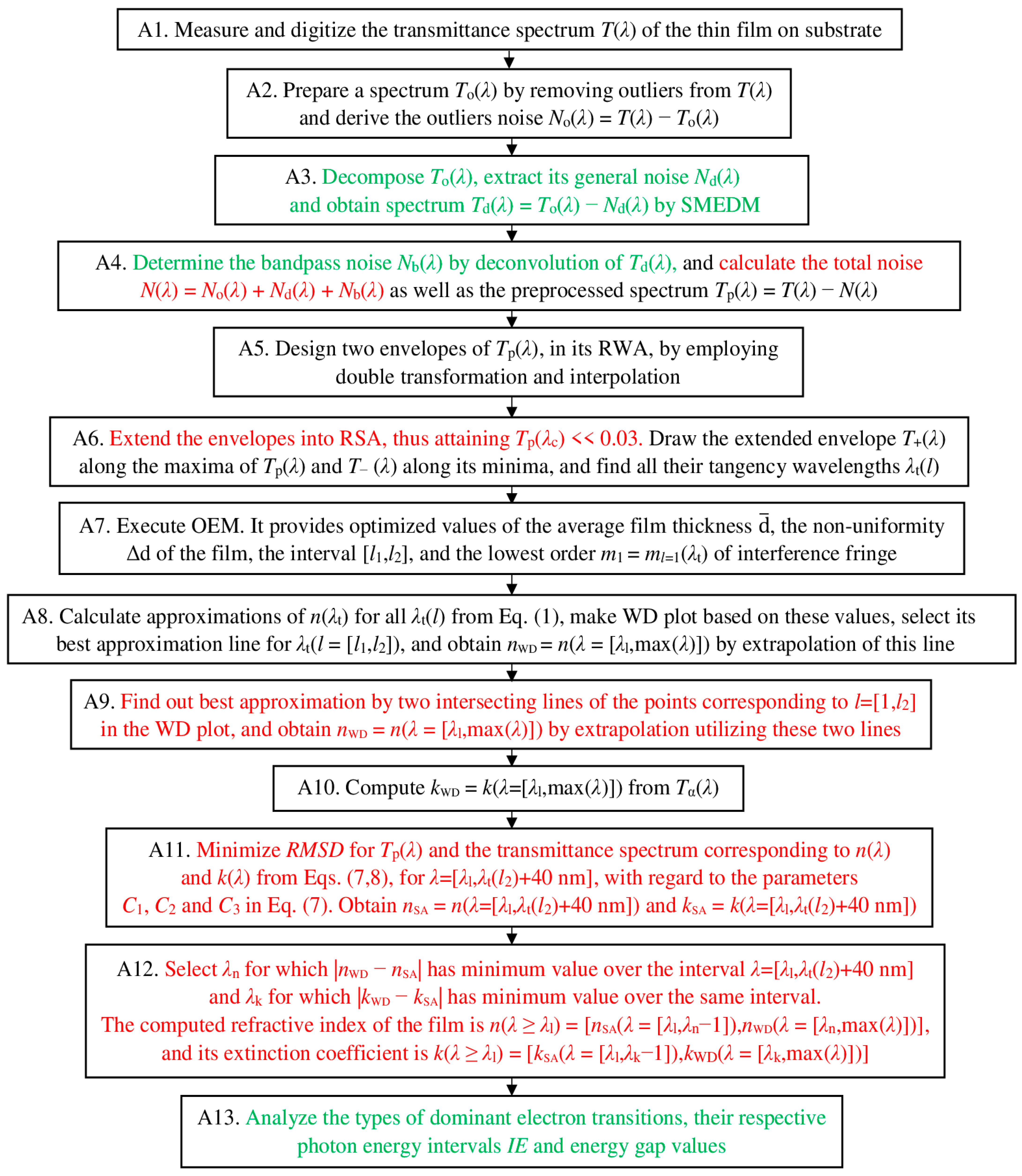
In addition, AEM and OEM are used here for wavelengths λ > λp, where Tp(λp) ≈ 2|N (λp)| and N(λ) is the total noise, because it is not plausible to draw envelopes in a spectral region where the noise dominates the transmittance spectrum. A flow chart of the algorithm of AEM is presented in Figure A1 in Appendix A. The execution of steps A2, A3, and A4 from the AEM algorithm allows analysis of the components of the total noise N(λ) and provides the preprocessed spectrum Tp(λ) to be utilized henceforth.
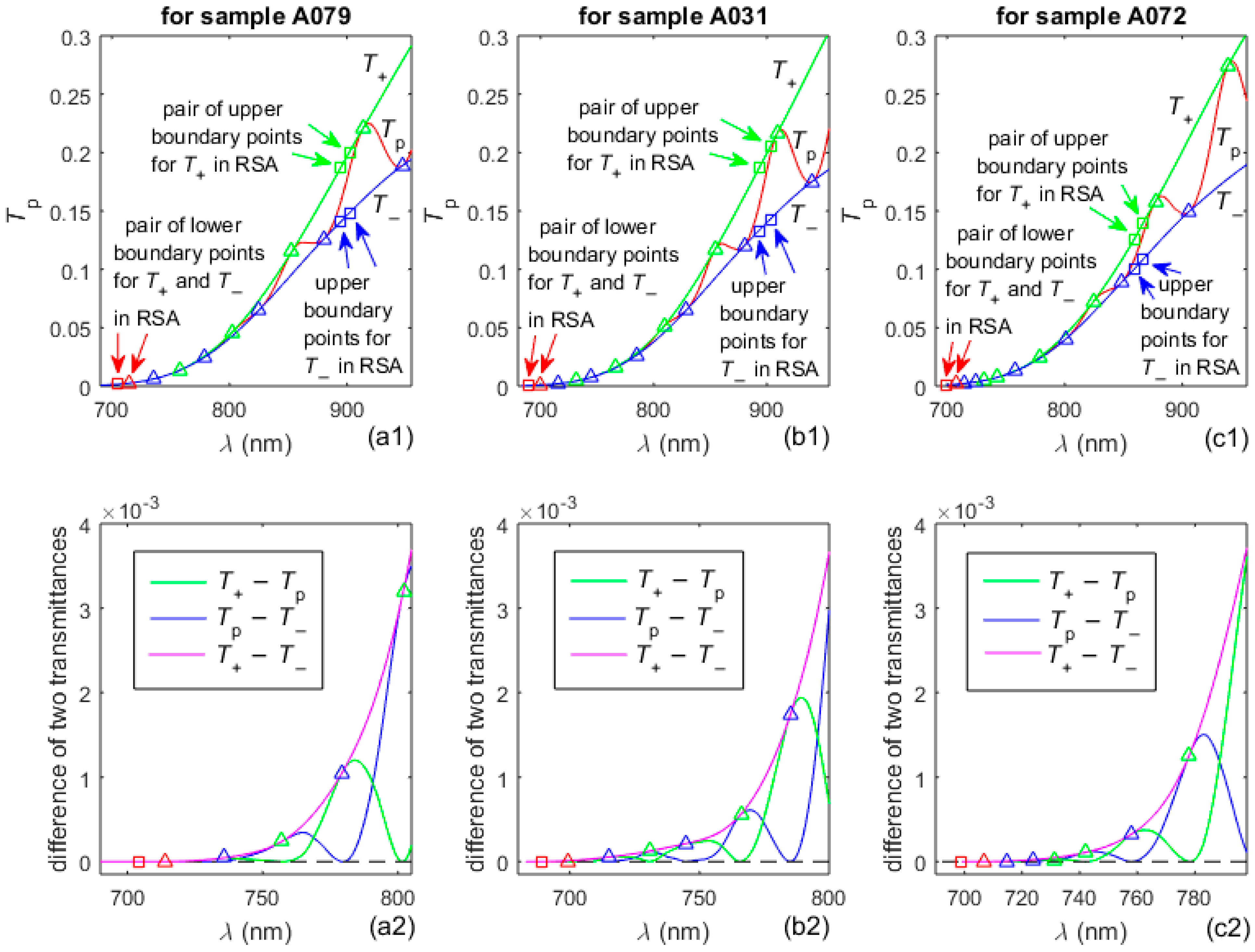
The main problem of drawing T+(λ) and T(λ) with Tc(λ) << 0.3 is that the difference between the envelopes is considerable over a wide RWA and drops super-exponentially for λ < λg, which hampers accurate determination of λt(λ) in the RSA [35]. To resolve this problem, extensions in the RSA are computed, utilizing the iterative approach from [36], for each one of the two envelopes already prepared in the RWA, as mentioned in step A6 from the AEM algorithm. However, the extension to the higher envelope has a pair of upper boundary points, selected from the known higher envelope in the RWA, so that their wavelengths split in three the interval [λt(l),λt(l + 1)] where λt(l) refers to the lowest or second lowest apparent maximum from the higher envelope in the RWA. The extension to the higher envelope also has a pair of lower boundary points selected from Tp(λ), with λh > λp for the lower of these points, and the wavelength distance between this pair of points is the same as for the pair of the upper boundary points. Moreover, the extension to the lower envelope has a pair of upper boundary points with the same wavelengths as those for the pair of upper boundary points in the extension to the higher envelope, and the pair of lower boundary points is identical to these for the extension to the higher envelope. The upper point from the pair of lower boundary points represents the convergence point Tp(λc) for the extended envelopes.
Notably, the two optimized intersecting lines in the WD plot, described in step A9 from the AEM algorithm, correspond to two undamped oscillators influencing Tp(λ) in its RWA.
The AEM utilizes the representation of n(λ) in the RSA by a second-order Cauchy equation:
n λ = C 1 + C 2 λ 2 + C 3 λ 4 ,
where C1, C2 and C3 are fitting parameters. In addition, the following new formula is derived for determination of k(λ) in RSA, by using the equations for Tp(λ), T+(λ) and T(λ) from [29], taking into account the substrate absorption:
k λ = λ W 1 λ 8 π 1 1 4 W 2 λ W 1 λ 2 ,
where
W 1 = τ a , f τ f , s τ s , a 2 x s ρ a , f 2 ρ f , s 2 ρ s , a x s 2 T i ,   W 2 = 1 ρ f , s ρ s , a x s 2 ρ a , f 2 ρ f , s 2 ρ s , a x s 2 ,   T i = 2 T + T T + + T , τ a , f τ f , s τ s , a = 8 ( n + 1 ) n ( n + n s ) 2 + k s 2 n s 2 + k s 2 ( n s + 1 ) 2 + k s 2 ,   x s = 4 π k s λ , ρ a , f = n 1 n + 1 ,   ρ f , s = ( n n s ) 2 + k s 2 ( n + n s ) 2 + k s 2 ,   ρ s , a = ( n s     1 ) 2 + k s 2 ( n s + 1 ) 2 + k s 2 ,
as pointed out in step A11 from the algorithm of the AEM. Since the previously discussed extension of the envelopes T+(λ) and T(λ) increases their accuracy, the extension should also increase the accuracy of k (λ) in the RSA from Equation (9), which implicitly includes Ti(λ) and both envelopes.
Furthermore, step A13 in the algorithm employs the derivatives of log10(αE) vs. E and −d[log10(αE)]/dE vs. E, rather than the very dependencies described in [50]. This leads to the use of smoother curve with flat regions, which can provide more accurate energy intervals IE of dominance of electron transitions with a particular value of q. Thereafter, the tangent to the Tauc function, from the Tauc plot for this value of q, is drawn at E corresponding to the average of the considered derivatives over IE, which should result in more accurate calculation of the respective energy gap. This energy gap is determined as the photon energy at which this tangent, to the Tauc function, crosses the axis E.

3.2. Experimental Features

Three samples are employed in this research, each one of them consisting of rf magnetron sputtered thin a-Si film on 1 mm-thick Corning Glass Eagle XG substrate. Argon gas was used in the sputtering process, while the gas pressure was 0.1 Pa for sample A079, 0.7 Pa for sample A031 and 1.1 Pa for sample A072. Normal incidence transmittance spectra of these samples were measured by a Perkin-Elmer Lambda 1050 UV/visible/NIR double-beam spectrophotometer providing illuminated film area of 10 mm × 3 mm, as 1 nm wavelength step of T(λ) is utilized in the present study. In addition, the following detectors were used in the measurement of such spectra: PbS detector for λ = [1801,2500] nm, InGaAs detector for λ = [861,1800] nm, and PMT detector for λ = [200,860] nm; λ decreased during the measurement [54]. Unlike in [54], though, the measured transmittance spectrum Ts(λ) and reflectance spectrum Rs(λ) of a bare substrate are also used in this study.

3.3. Preprocessing of the Transmittance Spectra T(λ)

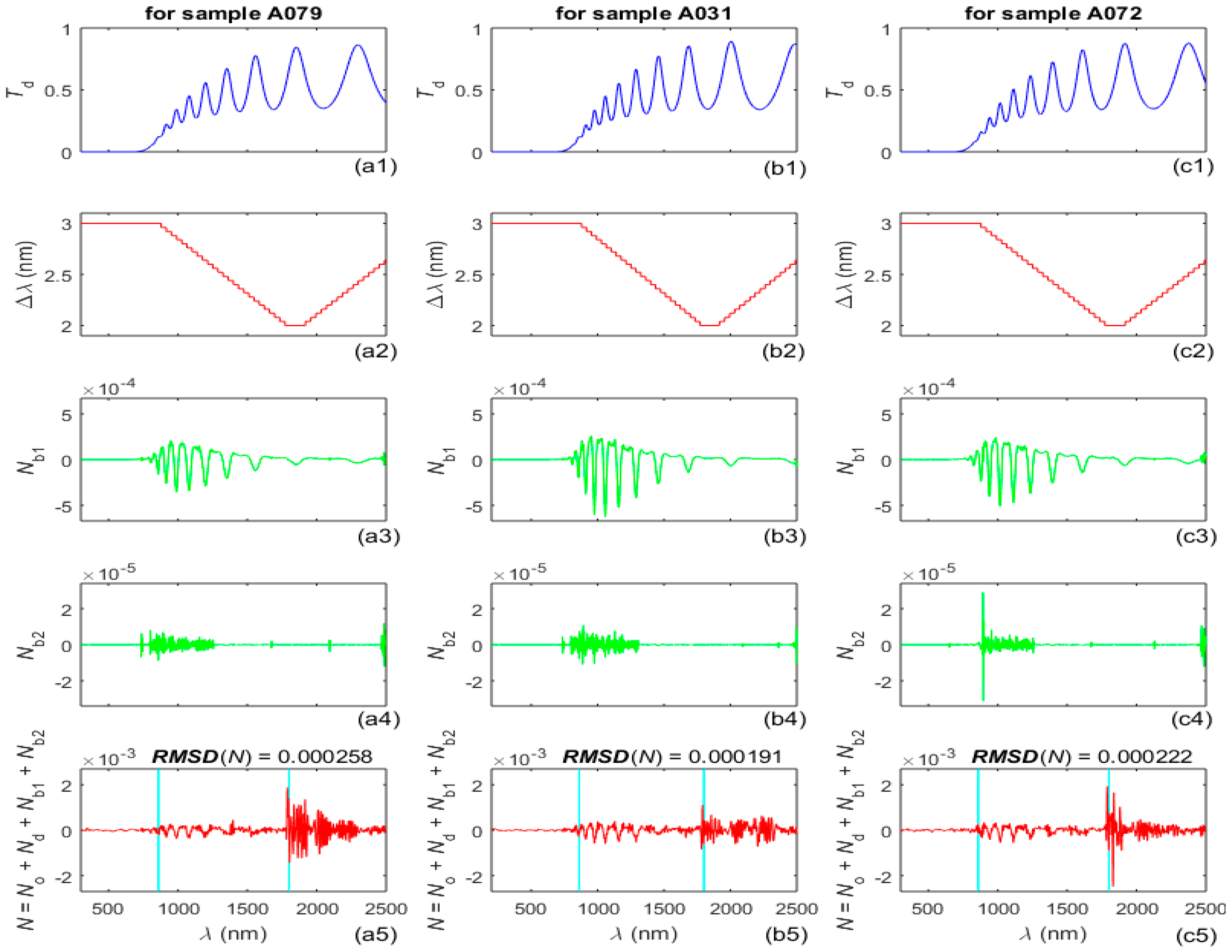
Outliers in T(λ) occur in many kinds of experimental datasets and can be removed, e.g., by the six sigma approach [58,59]. Regarding the general noise, our recent study demonstrated that superior denoising of UV-Vis-NIR spectra T(λ) of thin films is achieved by employing a method, abbreviated as SMEDM, based on complete ensemble empirical mode decomposition with adaptive noise (CEEMDAN) [60]. Also, spectrophotometers and spectroscopic ellipsometers usually contain monochromators with bandpass Δλ(λ), resulting in the presence of bandpass noise [61]. Yet, such monochromators typically have a triangular bandpass function, which allows calculation of the bandpass noise by using a formula from [62].
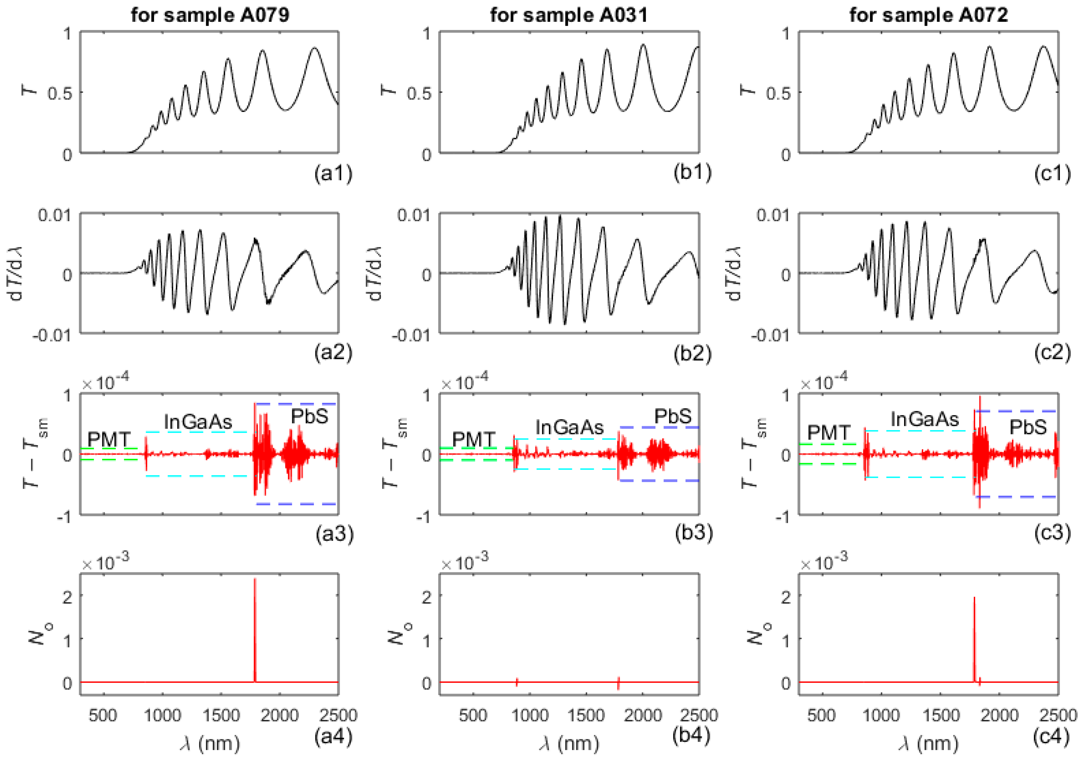
Graphs regarding characterization of the three studied a-Si films, by successive steps from the AEM algorithm in Figure A1, are presented in Figure 1, Figure 2, Figure 3, Figure 4, Figure 5, Figure 6, Figure 7, Figure A2 and Figure A3, where panels for A079 are in the first column, those for A031 are in the second, and those for A072 are in the third. With respect to the visualization of the results, in Figure 1, Figure 2, Figure 6, Figure A2 and Figure A3, the x-axis for each column is identical and labels are provided in the bottom row for clarity. The measured spectra T(λ), as well as results pertaining to the execution of step A2 from the AEM algorithm for determining the outlier noise No(λ) and the spectra To(λ) without outliers, are shown in Figure 1.
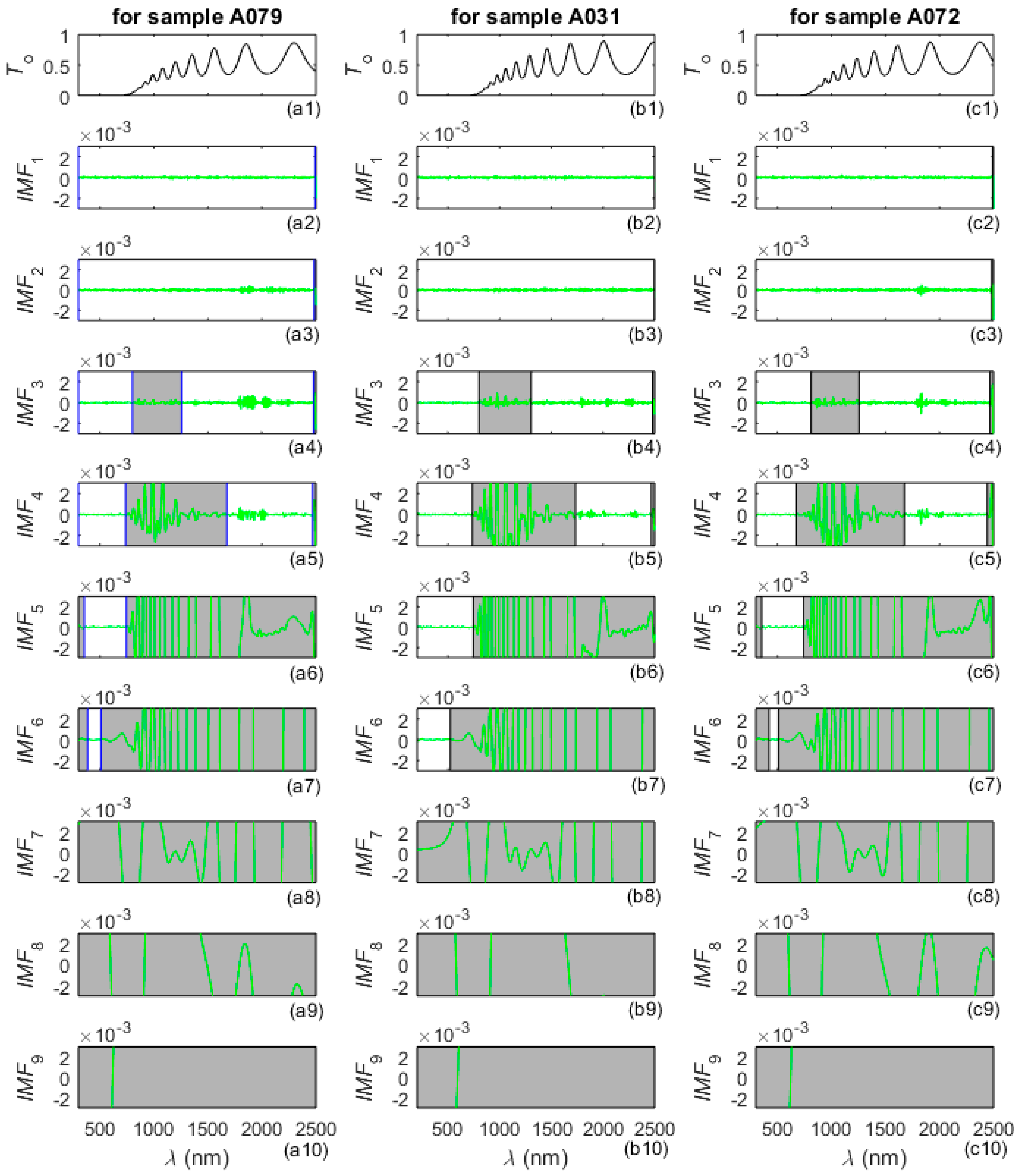
Following the results in [60], the decomposition of To(λ) is performed using CEEMDAN with 3500 realizations of auxiliary white noise and a magnitude of 0.2 adjusting these realizations. The intrinsic mode functions (IMFs) obtained by such decomposition of To(λ), and their spectral ranges with noise features, derived by SMEDM from [60], are illustrated in Figure A2 in Appendix A.
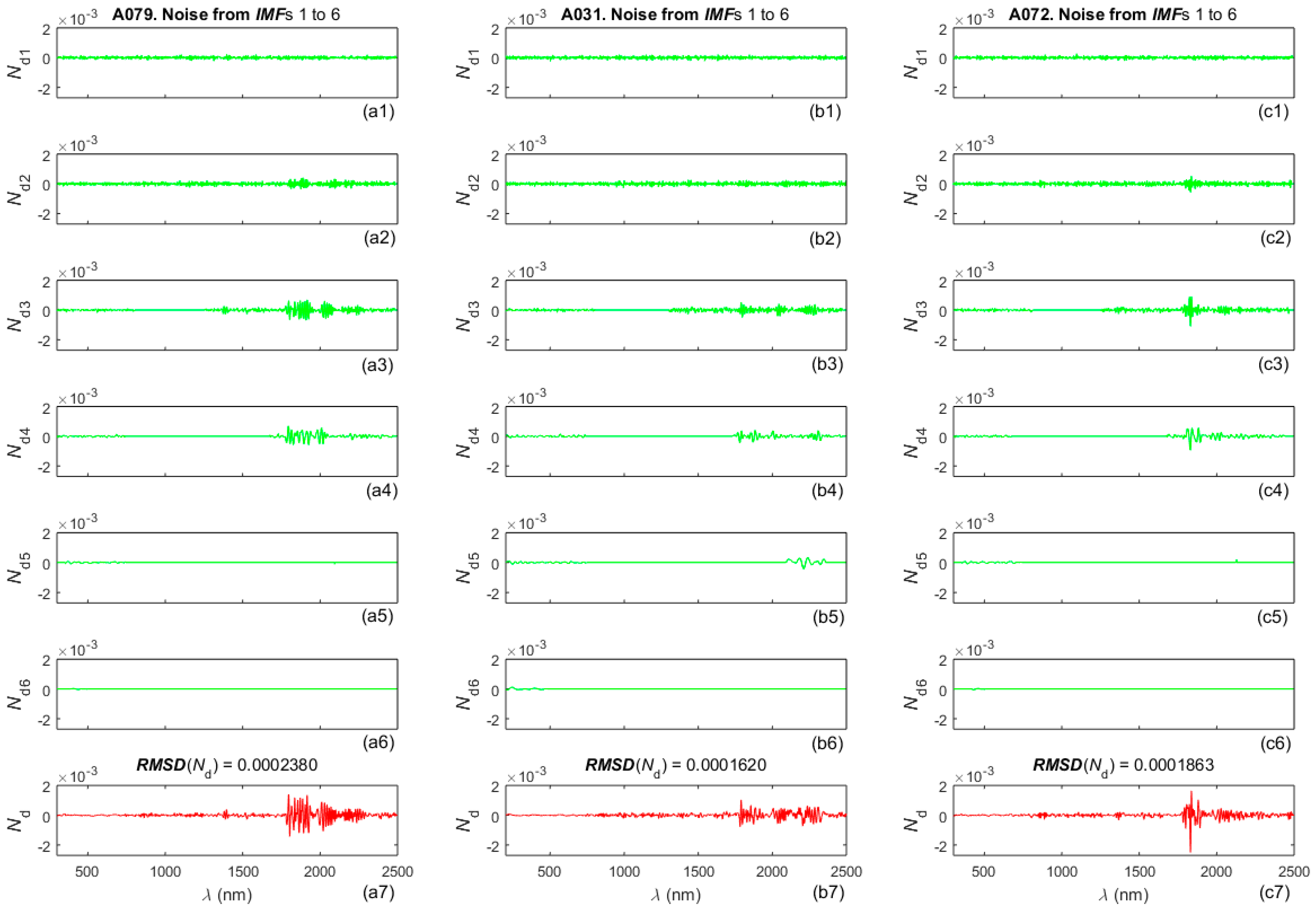
In Figure A3 in Appendix A3, we see the components of the general noise obtained from the IMFs with at least one area of noise features. The general noise Nd(λ) is a sum of these components, as is also shown in Figure A3, where RMSD(Nd) is the root mean square deviation of Nd(λ) over the entire measured spectrum. Actually, the individual IMFs of To(λ) differ for different runs of CEEMDAN; however, Nd(λ) remains virtually constant, as demonstrated in [60].
Graphs illustrating the determination of the bandpass noise Nb(λ) = Nb1(λ) + Nb2(λ) and the total noise N(λ), as described in step A4 from the AEM algorithm, are provided in Figure 2, where RMSD(N) is the root mean square deviation of N(λ) over the measured spectrum. Notably, the calculations of both the outlier noise No(λ) and the bandpass noise Nb(λ) do not employ adjustable parameters. The preprocessed spectrum Tp(λ) = T(λ) − N(λ) is used extensively henceforth, for each one of the samples A079, A031 and A072.
Figure 2. The spectra Td(λ) = To(λ) − Nd(λ) are in the first row of plots, the bandpass Δλ(λ) used in the measurements of T(λ) is in the second row, the first and second components of the bandpass noise (calculated as in [62]) are in the third and fourth rows, and the total noise is in the last row.
Nanomaterials 16 00522 g002

3.4. Computation of Extended Envelopes and Non-Dispersion Parameters of the Spectra and the Films

The two envelopes in the RWA of Tp(λ) are computed as in [36]. The new technique for extending these envelopes down to convergence point Tp(λc) << 0.03 from the RSA, mentioned in step A6 of the AEM algorithm, was described in Section 3.1. Graphs related to the preparation of the extensions to both envelopes into the RSA are shown in Figure 3.
Figure 3. Plots regarding the extensions to both envelopes of Tp(λ) into RSA; the black dashed line represents zero. The boundary points are exhibited by squares except for the convergence point Tp(λc) illustrated by red triangle. The tangency points T+(λt) and T(λt), between Tp(λ) and its extended envelopes, are represented by green and blue triangles, respectively.
Nanomaterials 16 00522 g003
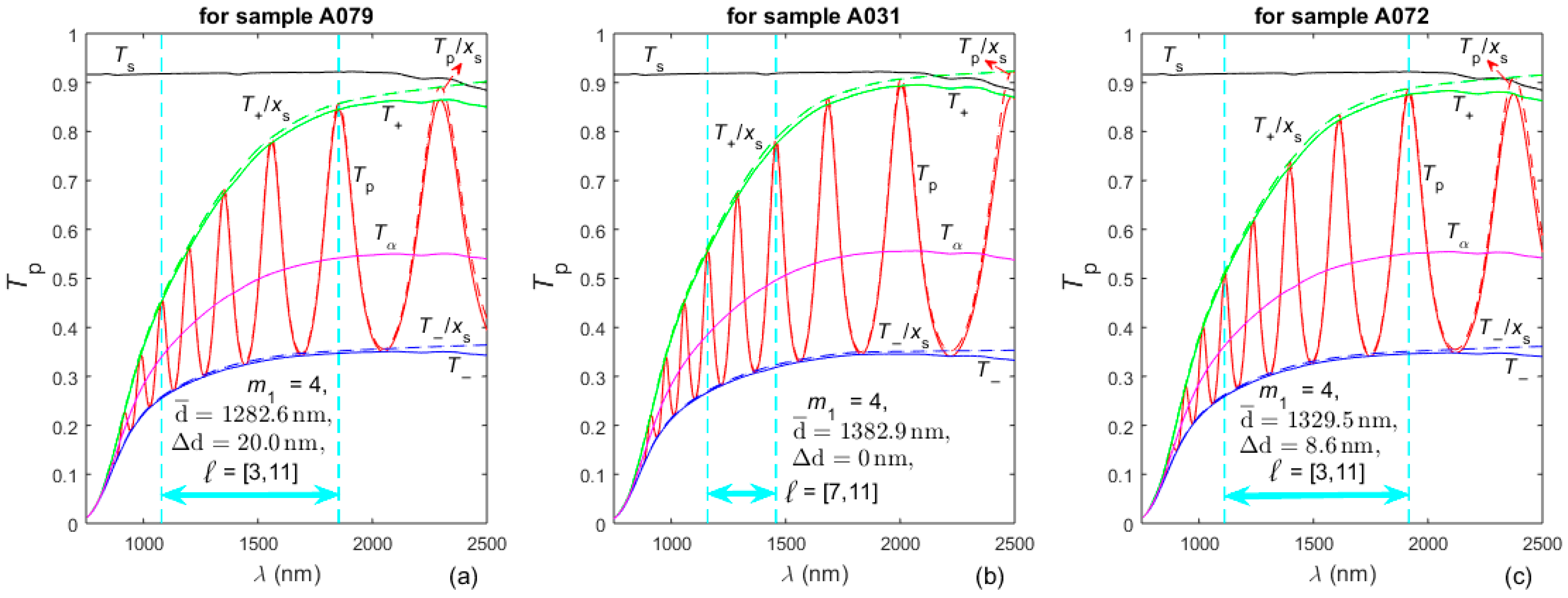
Figure 4. The spectrum Tp/xs and its envelopes T+/xs and T/xs are displayed by dashed lines, while the spectrum Tp(λ) and its envelopes T+ and T are drawn as solid lines. The OEM-computed optimized values of d ¯ , ∆d, m1, and l = [l1,l2] are also included, and the wavelength interval corresponding to these l values is represented by double arrow.
Nanomaterials 16 00522 g004
OEM is performed as described in [42]. Graphs showing the extended envelopes T+(λ) and T(λ) and results from the OEM are presented in Figure 4. As seen from Figure 4, Ts(λ) decreases for λ > 2000 nm. This indicates that there is absorption in the substrate for these wavelengths, i.e., ks(λ) should be taken into account for accurate characterization of the three a-Si films, which was not done in [54]. With respect to this and a comment from Section 1, the curves T+(λ)/xs(λ) and T(λ)/xs(λ) included in the double transformation of Tp(λ) used in the OEM are not distorted for λ > 2000 nm; however, their corresponding envelopes T+(λ) and T(λ) are distorted there. Notably, the results from the OEM indicate that the films A079 and A072 are non-uniform, since their ∆d > 0, although they were considered as being uniform in [54].

3.5. Results Regarding n(λ), k(λ), and fvoids

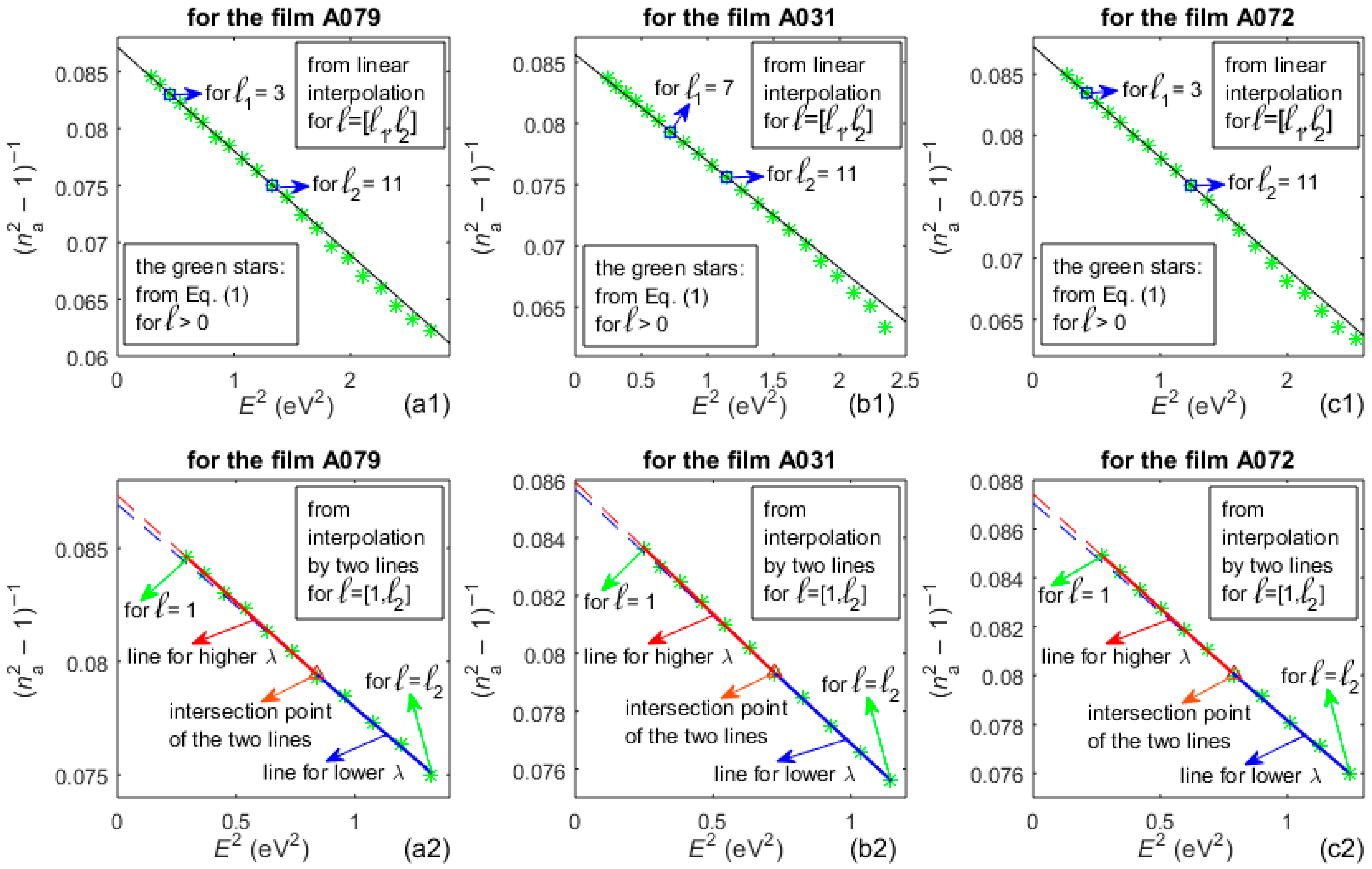
According to the text from Section 1, the essence of step A8 from the AEM algorithm is illustrated by the graphs in the first row in Figure 5, while the graphs in the second row represent step A9 of this algorithm.
Figure 5. WD plots with green stars corresponding to na(λt). The first row from these plots refers to common fitting by one line of the dependence (na2 − 1)−1 vs E2, only for λt(l = [l1,l2]) obtained from OEM. The second row is for fitting by two intersecting lines of (na2 − 1)−1 vs E2, only for λt(l = [1,l2]).
Nanomaterials 16 00522 g005
The dependencies nWD(λ = [λp,max(λ)]) and kWD(λ = [λp,max(λ)]) are calculated from these fitted lines in the WD plot and Tα(λ), respectively, as described in steps A8 to A10 from the AEM algorithm. Next we compute nSA(λ ⊂ RSA) and kSA(λ ⊂ RSA), according to step A11, followed by determination of n(λ = [λp,max(λ)]) and k(λ = [λp,max(λ)]) as explained in step 12.
Furthermore, TLU as well as UDM parametrizations, including d ¯ and ∆d as unknowns, are performed by using Tp(λ). In the TLU parametrizations, we assume the physically plausible boundary condition ε(E → ∞) = 1 for the dielectric function ε, as discussed in [51]. The employed UDM is based on the formalism from [52], and includes one excitonic term of interband transitions since the utilization of one-oscillator DMs has been considered successful for characterization, from T(λ), of other rf magnetron sputtered thin a-Si films [64,65]. In addition, high-energy excitations of valence electrons are excluded from the UDM, because such excitations occur at photon energies E > Eh/4 + 3Eg/4 which are higher than max(E) for our measured spectra. Instead, a pole, representing a high-energy Lorentz oscillator with vanishing broadening, is introduced in the UDM by adding a term Np/(Ep2E2) to ε, as explained in the spectroscopic ellipsometry study [66]. The respectively computed TLU and UDM parameters are exhibited in Table 1.
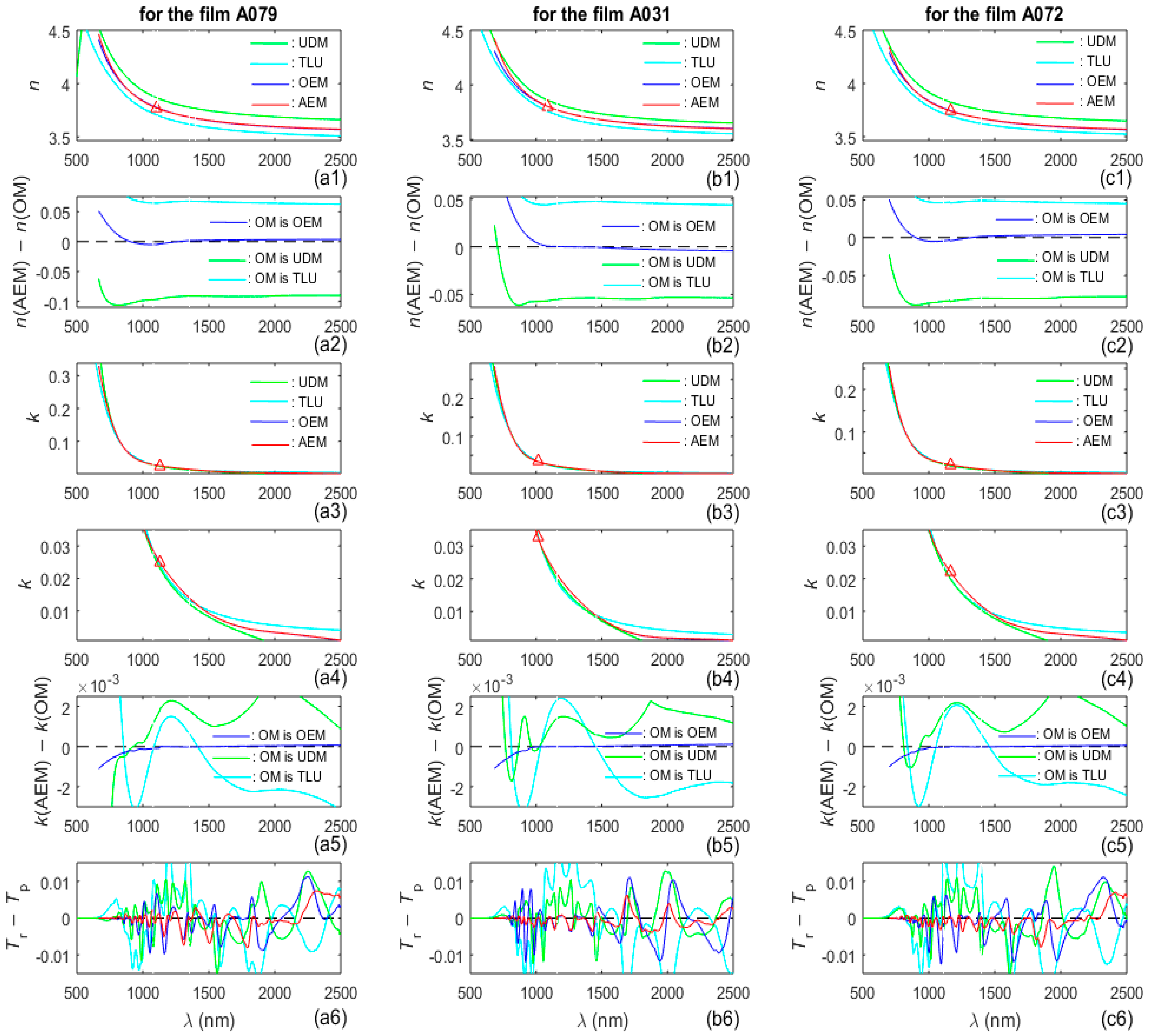
Plots including n(λ) computed by the TLU, UDM, OEM, AEM and their mixed differences, as well as k(λ) computed by the TLU, UDM, OEM, AEM and their mixed differences, are included in Figure 6.
Figure 6. Drawings concerning n(λ) and k(λ) computed by TLU, UDM, OEM, and AEM. In the first row of graphs, the red triangles denote n(λn), while the red triangles in the third and fourth row show k(λk). The plots from the fourth row are magnified images, in RWA, of these from the third row. Each curve with a particular color from the sixth row corresponds to the method represented by a curve with the same color in the first row.
Nanomaterials 16 00522 g006
After completing a particular a-Si film characterization, the respective reconstructed spectrum Tr(λ) can be computed, along with the corresponding FOMs from Equation (5), for different wavelength intervals. Such FOMs, for λ ⊂ [λp,λ(l2)] representing RSA, λ ⊂ [λ(l2),λ(l1)] for intermediate absorption in the film (RIA), and λ > λ(l1) corresponding to the RWA, are included in Table 2.
The volume fractions fvoid of voids in the a-Si films are calculated from Equation (7) by using E0, Ed, and n0 corresponding to the dashed red lines from the plots in the second row of Figure 5, i.e., n(λ) computed by the AEM. The values of these parameters are shown in Table 3.
Table 2. Results regarding the accuracy of characterization of the a-Si films by several characterization methods. The data in the third column are derived from Equation (1).
Film d ¯  (nm), Δd (nm);
Source
RE ( d ¯ ) (%);
Source
MethodFOM
[λl,λ(l2)]
FOM
[λ(l2),λ(l1)]
FOM
[λ > λ(l1)]
FOM
[λl,max(λ)]
A0791299, 0;
EM from [54]
0.850;
EM from [54]
OEM2.804.234.564.20
AEM0.822.903.843.30
1282.6, 20.0;
AEM
0.0652;
AEM
TLU7.1613.07.158.32
UDM3.196.376.005.60
A0311359, 0;
EM from [54]
0.662;
EM from [54]
OEM3.862.016.095.08
AEM1.091.592.331.96
1382.9, 0;
AEM
0.1028;
AEM
TLU8.8115.410.210.9
UDM3.894.825.434.97
A0721310, 0;
EM from [54]
0.992;
EM from [54]
OEM3.893.515.644.99
AEM1.101.743.232.68
1329.5, 8.6;
AEM
0.0504;
AEM
TLU6.9414.58.219.25
UDM3.536.256.215.72
Table 3. Computed data regarding the determination of the volume fractions fvoid (%) of voids, based on the results for n(λ) derived by AEM.
FilmE0Edn0fvoid (%)
A0793.0434.93.536.68
A0313.0735.73.565.65
A0723.0635.03.536.75
Furthermore, Equation (6) is reworked for the cases when a film from a given material contains a second medium, e.g., consisting of volumes containing particular molecules or molecular complexes, instead of gaseous voids. The volume fraction fsm of the second medium is derived similarly to Equation (7), whereby:
f s m     n z 0 2 + 2 n 0 2 n y 0 2 n 0 2 3 n 0 2 n y 0 2 n z 0 2 × 100 ( % ) ,
where nz0 = nz(E → 0) is the static refractive index of the pure second medium. Equation (10) represents a generalization of Equation (7), and it is not used in this paper; however, it is available for future studies.

3.6. Results Related to k(λ) Computed by AEM

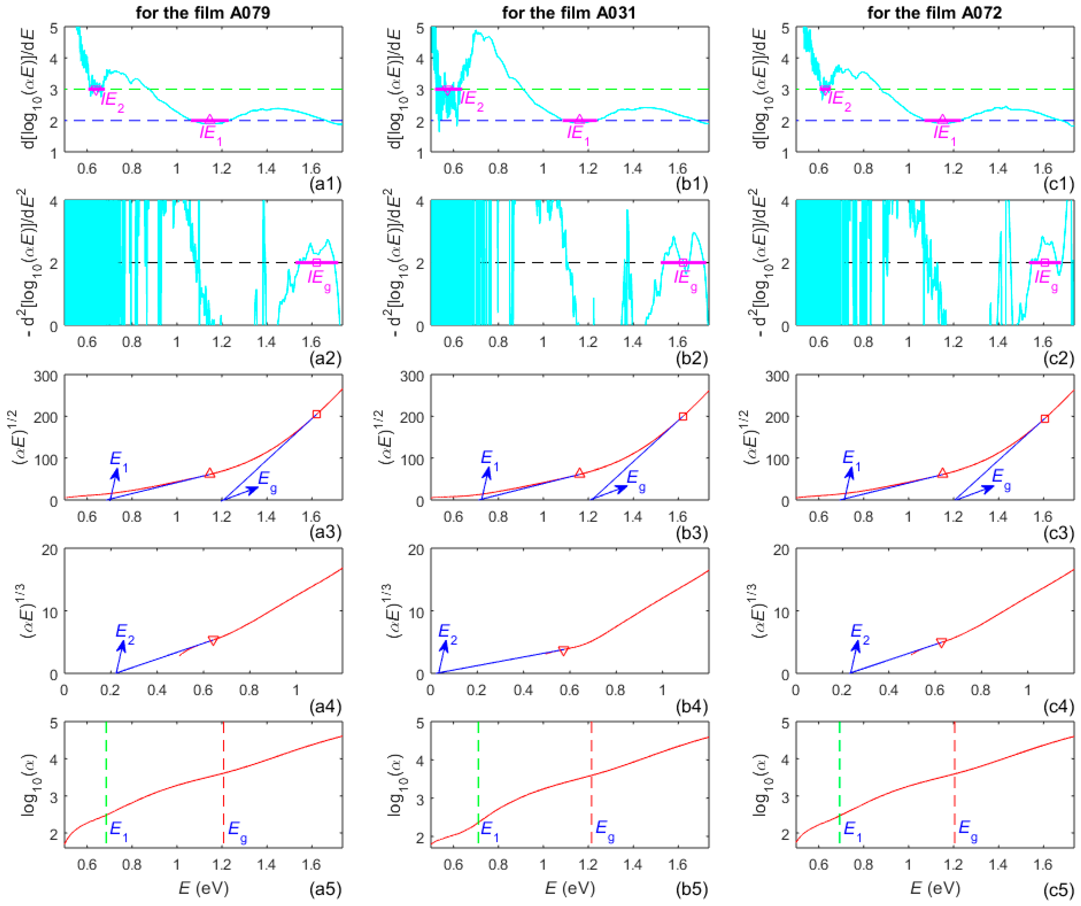
Several dependencies for determination of the dominant electron transitions in the three a-Si films, the energy intervals IE of dominance of these transitions, and their energy gaps, described in Section 1, are included in Figure 7.
The energy gap with largest value, amongst the three energy gaps from the third and fourth row in Figure 7, corresponds to the largest absorption coefficient α(λ). Therefore, it is the bandgap for electron transitions from the valence band to the conduction band, which is commonly designated as Eg. Values of q, as well as their respective energy intervals IE and energy gaps, are calculated from Figure 7, and are presented in Table 4.
Figure 7. Graphs related to Tauc plots and Urbach plots using k(λ) obtained by AEM. The magenta segments from the panels in the first and second row represent IE for different q in Equation (3). Each magenta triangle or square in these panels corresponds to the photon energy E where the tangent is drawn to the respective Tauc function from the third or fourth row.
Nanomaterials 16 00522 g007
Table 4. Values of q, energy intervals IE of dominance of electron transitions with these values of q, and energy gaps E2, E1 and Eg for these transitions.
FilmqIE2 (eV)E2 (eV)qIE1 (eV)E1 (eV)qIEg (eV)Eg (eV)
from Figure 7
Eg (eV)
from [54]
A0793[0.612,0.672]0.2192[1.07,1.22]0.6852[1.53,1.71]1.211.23
A0313[0.525,0.632]0.0212[1.09,1.23]0.7162[1.53,1.72]1.211.24
A0723[0.611,0.647]0.2292[1.08,1.23]0.6932[1.54,1.67]1.211.24

4. Discussion

A comparison between the noise components No(λ), Nd(λ), Nb(λ), and the total noise N(λ), included in Figure 1, Figure 2, Figure A2 and Figure A3, indicate that the detectors are the main source of noise in T(λ) of the a-Si films, as the PbS detector introduces most noise, followed by the InGaAs detector. In addition, it is seen from the graphs in the third and fourth row of Figure 1 that spikes of outlier noise usually occur just below 1800 nm, i.e., after the replacement of the PbS detector by the InGaAs detector. The magnitude of the bandpass noise increases with decreasing distance between adjacent λt, and this magnitude is significantly smaller than those for Nd(λ) and No(λ), as seen in Figure 1, Figure 2 and Figure A3. The plots from the last row of Figure 2 also show that the magnitude of the total noise is largest around 1800 nm, where the PbS detector is replaced by the InGaAs detector, whereby this magnitude does not exceed 2.5 × 10⁻³. Since the primary source of systematic measurement error in T (λ) relevant to this study is the very small stray light error, which is <1.5 × 10⁻⁶ [67], this error is disregarded in this paper.
In the preparation of the extended envelopes of Tp(λ) convergence points Tp(λc) are achieved with the following values: 2.00 × 10⁻³ for A079, 4.47 × 10⁻⁴ for A031, and 1.38 × 10⁻³ for A072. These values do not exceed 2.00 × 10⁻³, indicating that in this study we attained the required drawing of envelopes with Tp(λc) << 0.03.
In EMs, d ¯ is computed first, followed by n(λ), and then k(λ), which means that accurate determination of d ¯ is needed for accurate characterization of thin films by envelope methods. With respect to this, the data from the third column of Table 2 indicate that the average value of RE( d ¯ ) is 0.835% for the characterizations of the three a-Si films studied here, from [54], by the EM of Swanepoel for uniform film on transparent substrate [38]. From the same column in Table 2 we also see that the average value of RE( d ¯ ) is 0.0728% for the characterizations of these films by the AEM proposed here. Therefore, the AEM leads on average to 11.5-times-smaller relative error in the computation of d ¯ for these a-Si films, with respect to the EM from [38]. In addition, the data from the second column in Table 2 show that using the AEM, compared to the EM from [38], results in the following relative differences in the computed d ¯ : −1.26% for A079, 1.76% for A031 and 1.49% for A072. As a comparison, the thickness of the film A031 was measured by a Dektak surface profiler to be 1385 nm, and by SEM to be 1348 nm in [54], while this study provides that d ¯ = 1382.9 nm, as shown in Figure 4b.
As seen from the WD plots in the first row of Figure 5, the vast majority of the green stars in the RSA are positioned below the black line. This is due to the fact that the function (n2 − 1)−1 is inversely proportional to both Ed and the intensity of the strong interband electron transitions, as seen in Equation (2). Similarly, the shallower slope of the blue lines in RIA compared to their respective red lines in the RWA, in the graphs from the second row in Figure 5, indicates a stronger intensity of the electron transitions via tail states than via dangling bond states. This shows that tail states have a higher concentration than dangling bond states in the studied a-Si films.
The fact that most green stars in the RSA in Figure 5 are located below the black line also indicates that n(E) should be larger in the RSA than the value used in the OEM. Indeed, n(AEM) > n(OEM) in the RSA, according to the respective lines from the first row of graphs in Figure 6. In addition, the graphs in the fourth row in Figure 6 illustrate that k(UDM) < 0 in the RWA and k(TLU) is significantly larger than k(AEM) ≈ 0 in the RWA. Since previous studies have shown that k(λ) ≈ 0 in the RWA of a-Si [42,68], the above results indicate that both the UDM and TLU provide inaccurate characterization of the a-Si films in the RWA.
In the text after Equation (5), it is commented that a smaller FOM calculated over some wavelength region corresponds to more accurate thin film characterization over this region. In connection with this, amongst the 48 FOM data, shown in the last four columns in Table 2, there are 12 for each of the four employed characterization methods; whereby these 12 FOM data refer to the three a-Si films and the four spectral regions covering all λ > λl. A comparison in corresponding manner of the four sets of 12 FOM data, for these four methods, shows that utilizing the TLU leads to the largest values for all 12 FOM data, while the AEM provides the smallest values for all 12 FOM data. Moreover, the OEM gives 9 penultimate smallest FOM data and UDM—3 penultimate smallest FOM data. Furthermore, the ratio [FOMav(OEM) − FOMav(AEM)]/FOMav(OEM) ≈ 44.4%, where FOMav is an average over the three films of the respective FOMs from the last column in Table 2, and represents a relative decrement in the error of characterization by the AEM compared to the OEM.
The results from the previous three paragraphs show that the AEM provides the most accurate characterization of the three a-Si films, in each one of the three studied regions from their spectra Tp(λ > λp), and the TLU provides the least accurate characterization of these films in these regions. Therefore, this justifies the use of n(λ) and k(λ), computed by the AEM, as inputs for the preparation of Table 3, Figure 7, and Table 4.
In respect to the above, the AEM results from the second column of Table 2 and the last row from Figure 2 demonstrate the following relationship for the three studied films: the thicker the film, the smaller its non-uniformity ∆d, and the smaller the noise N(λ) in its measured spectrum T(λ).
According to the data from Table 3, the studied a-Si films contain voids, with quite low volume fractions fvoid = [5.65,6.75]%, unlike the conclusion from the less accurate characterization in [54] that these films do not contain voids. In addition, sensitivity analysis shows that fvoid has similar sensitivities to errors in ny0 and n0. Moreover, the relative error in fvoid increases almost linearly with errors in ny0 and n0, and this relative error does not exceed 14.2% when the absolute errors in both parameters remain below 0.01. With regard to this, results from [54] indicated that, in general, a decreasing volume fraction of voids fvoid in magnetron sputtered a-Si films is associated with increases in both the static refractive index n0 and the extinction coefficient k(λ).
Notably, it has been concluded in [64] that the TLU with an Urbach tail formulated by an equivalent of Equation (4), as in [51], provides proper characterization of other magnetron sputtered a-Si films. Additionally, FOM[λl,max(λ)] = [5.55,12.67], with T(λ) included in Equation (5) instead of Tp(λ), was obtained in [64] for the same TLU applied to other a-Si films, which is commensurate with FOM[λl,max(λ)] = [8.32,10.9] for this TLU, which is seen from the last column in Table 2. Since results from the present work already showed that this TLU leads to the least accurate characterizations, employing the Urbach tail expressed by Equation (4) over the entire subgap region is clearly inaccurate for the studied a-Si films. Taking into account the linearity of log10(α) vs. E < Eg from Equation (4), this assumption is supported by the apparent absence of a straight line approximation of this dependence, for all E < Eg, from the graphs in the last row of Figure 7.
Nevertheless, the linear parts of the curves in the graphs in the last row of Figure 7, for E just below Eg, represent the Urbach tail region, where the electron transitions are via tail states. According to Equation (4), the Urbach energy EU can be calculated from the slopes of these linear parts, yielding EU = 288 meV for the film A079, EU = 274 meV for A031, and EU = 277 meV for A072. However, the non-linear parts of the above-mentioned curves, for E below the Urbach tail region, represent the dangling bond region, where the electron transitions occur mainly via dangling bond states.
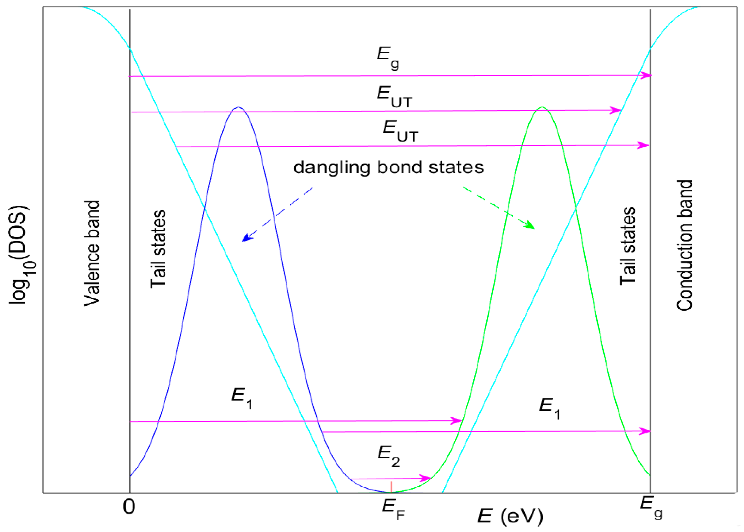
Furthermore, the types of electron transitions featured in T(λ) are determined taking into account Equation (3), the graphs from the first two and last rows of Figure 7, and Table 4. Accordingly, these transitions are: indirect allowed transitions above the bandgap Eg = 1.21 eV, indirect transitions via tail states with energy EUT just below Eg, indirect allowed transitions with energy gap E1 = [0.685,0.693] eV, and indirect forbidden transitions with energy gap E2 = [0.021,0.229] eV. In addition, the energy intervals IE of dominance of these electron transitions contain significantly higher energies compared to the energies of optical phonons in a-Si [68]. The above data can be explained by the drawing regarding the density of states (DOS) depicted in Figure 8.
The representation of the DOS in Figure 8 is consistent with the Mott–Davis model for amorphous materials [12], as well as with the involvement of electronic transitions via both tail states and dangling bonds. In this model, tail states are caused by structural disorder, because the bond angles and bond lengths vary slightly from the ideal crystalline values. This strains the network, pushing some states from the edges of the valence and conduction bands into the band gap. On the other hand, a dangling bond occurs in a semiconductor with predominantly tetrahedrally coordinated atoms, such as a-Si, when an atom has only three neighbors, leaving one electron unbonded. Dangling bonds create deep levels near the center of the band gap, where lower energy states correspond to dangling bonds occupied by single electrons and higher energy states represent dangling bonds occupied by two electrons [12]. Furthermore, the Fermi level EF is fixed between the energies of these two types of dangling bond states, whereas the electronic states below EF are mostly occupied, while those above EF are mostly unoccupied prior to irradiation by a spectrophotometer’s light [14].
Importantly, electronic transitions via both tail states and dangling bond states have not been included in any DM utilized for spectroscopic characterization of a-Si from one measured UV-Vis-NIR spectrum, most likely because the concentration of dangling bond states in a-Si is significantly lower than that of tail states [68,69]. Furthermore, sequential parametrization can achieve a better accuracy of film characterization than simultaneous parametrization, provided it is feasible, due to improved convergence and reduced sparsity-induced instability [70]. Therefore, the successful analysis of transitions via dangling bonds in this study can be associated with the sequential computation of d ¯ , ∆d, n(λ) and k(λ) by AEM, compared to the simultaneous computation of many model parameters by the dispersion model-based TLU and UDM.
In addition, another two magnetron sputtered a-Si films were also parametrized by the UDM, from a quasi-normal incidence reflectance spectrum R(λ) of the sample [71]. The lowest FOMs reported in [71] for these films were 5.18 and 5.46, respectively, which is significantly larger than the FOMs obtained in this paper by the AEM. Yet other magnetron sputtered a-Si films have been parametrized in [72] by reflectance spectroscopic ellipsometry (measuring the change in light’s polarization state) and the Cody–Lorentz dispersion model, thus not providing a FOM corresponding to Equation (5). Importantly, though, it has been assumed in both [71,72] that a single oscillator model describes the behavior of T(λ > λg), which is shown to be insufficiently accurate by the present study.
The FOMs obtained by the AEM and reported in Table 2 are record lows, which indicates that the AEM can be used for improved design in relatively new practical applications of a-Si films. These include high-density memory devices based on spintronics [73,74], next-gen solar power (PV-EC systems for hydrogen) [75], advanced LiDAR for autonomous vehicles [76], silicon photonics for AI/data centers/telecoms (like 6G) [77], and improved battery anodes for EVs [78]. In addition, the AEM can be used to characterize thin films with different chemical compositions, e.g., graphene films similar to those from [79,80], as long as they provide an interference transmittance spectrum T(λ) with at least five extrema, in accordance with results from [41].

5. Conclusions

This paper reports the development of an advanced envelope method (AEM) for accurate characterization a single thin film on a thick substrate using its UV-Vis-NIR transmittance spectrum, T(λ). The AEM includes the following theoretical novelties: improved preprocessing of T(λ), drawing envelopes deeper into RSA, using two lines in the WD plot for the computation of n(λ) in the RWA, and employing both the Cauchy equation and a new formula for determination of n(λ) and k(λ) in the RSA.
It is demonstrated that the AEM provides most accurate characterization of three a-Si films, compared to the OEM, TLU and UDM; the relative decrement of the characterization error by the AEM is ≈44.4%, on average for these three films, compared to the OEM, which shows the second best results. In fact, the FOMs obtained from the AEM characterizations in this study are the lowest recorded compared with all previously published characterizations of magnetron sputtered thin a-Si films. This indicates that the most accurate characterizations of such films are the characterizations by the AEM reported here.
As a result of significantly decreased characterization errors in the AEM, especially for k(λ), four different types of electron transitions are identified in the three a-Si films. The respective energy gaps are calculated, and the DOS is interpreted to be consistent with the Mott–Davis model for amorphous semiconductors. Notably, analysis of electron transitions via dangling bonds and description of intricate DOSs have not been possible in the framework of the EM. Importantly, the AEM results reported here represent the first characterizations of a-Si films that account for electronic transitions via both the tail states and dangling bond states, using only spectroscopic ellipsometry or spectrophotometry in the UV-Vis-NIR region.
Since the studied a-Si films contain voids with the volume fraction fvoid = [5.65, 6.75]%, they represent a nanostructured material with an internal nanoscale surface structure. In addition, fvoid should be proportional to the concentration of dangling bonds in these films, as indicated in [81]. On the other hand, dangling bond states mostly act as non-radiative centers that trap charge and reduce mobility, unlike tail states [69,82]. These factors highlight the importance of the separate analysis of dangling bond states from tail states, as achieved in this research.
In future, the AEM can be used for characterization of thin films with different compositions, and it can also be expanded to include more oscillators in the RWA and RIA. Furthermore, the novel Equation (10) can be used for calculation of the volume fraction fsm of the second medium (e.g., consisting of volumes containing particular molecules or molecular complexes), applicable not only for films, but for any mixture of two media.

Author Contributions

Conceptualization, D.M. and M.B.; methodology, D.M. and E.M.; software, D.M. and R.R.; validation, M.B. and S.F.; formal analysis, D.M. and G.A.; investigation, D.N.; resources, G.A.; data curation, M.B. and S.F.; writing—original draft preparation, D.M. and M.B.; writing—review and editing, E.M.; visualization, D.N.; supervision, G.A.; project administration, R.R.; funding acquisition, G.A. All authors have read and agreed to the published version of the manuscript.

Funding

This research was funded by the European Regional Development Fund within the operational program “Bulgarian national recovery and resilience plan”, procedure for direct provision of grants “Establishing of a network of research higher education institutions in Bulgaria”, under Project BG-RRP-2.004-0005 “Improving the research capacity and quality to achieve international recognition and resilience of TU-Sofia (IDEAS)”.

Data Availability Statement

The original contributions presented in this study are included in the article. Further inquiries can be sent to the corresponding author.

Conflicts of Interest

The authors declare no conflicts of interest. The funders had no role in the design of the study; in the collection, analyses, or interpretation of data; in the writing of the manuscript; or in the decision to publish the results.

Abbreviations

The following abbreviations are used in this manuscript:
CEEMDANcomplete ensemble empirical mode decomposition with adaptive noise
UV-Vis-NIRultraviolet–visible–near-infrared
EMenvelope method
RWAregion of weaker absorption in the film
RIAregion of intermediate absorption in the film
RSAregion of stronger absorption in the film
WD plotWemple–DiDomenico plot
DMdispersion model
TLUTauc–Lorentz–Urbach dispersion model
UDMuniversal dispersion model
OEMoptimizing envelope method
AEMadvanced envelope method
RMSDroot mean square deviation
FOMfigure of merit
RErelative error
DOSdensity of states

Appendix A

Figure A1. Algorithm of AEM for characterization of thin films from their T(λ). The text in green represents elements which have not been published in studies including thin film characterization, while the text in red highlights novelties of this algorithm. Steps A1 and A2 are executed as in [60], step A5— as in [36], steps A7 and A8—as in [42], and a technique from [50] is used at step A13.
Nanomaterials 16 00522 g0a1
Figure A2. The spectra To(λ) and IMFs from their decomposition by CEEMDAN. The areas with bumpy IMFk(λ) are shaded in gray and contain signal features, while those with flattish IMFk(λ) are in white and contain noise features, according to SMEDM [31].
Nanomaterials 16 00522 g0a2
Figure A3. Components Nd1(λ) to Nd6(λ) of the general noise, extracted from their respective IMFs with at least one white area in Figure 3 (following SMEDM [31]), and the general noise Nd(λ) drawn in red.
Nanomaterials 16 00522 g0a3

References

  1. Jun, B.H. Advanced optical materials: From materials to applications. Int. J. Mol. Sci. 2023, 24, 15790. [Google Scholar] [CrossRef]
  2. Al-Amri, A.M. Recent progress in printed photonic devices: A brief review of materials, devices, and applications. Polymers 2023, 15, 3234. [Google Scholar] [CrossRef]
  3. Wang, H.; Chen, L.; Wu, Y.; Li, S.; Zhu, G.; Liao, W.; Zou, Y.; Chu, T.; Fu, Q.; Dong, W. Advancing inorganic electro-optical materials for 5 G communications: From fundamental mechanisms to future perspectives. Light Sci. Appl. 2025, 14, 190. [Google Scholar] [CrossRef]
  4. Andrade, P.H.; Volkringer, C.; Loiseau, T.; Tejeda, A.; Hureau, M.; Moissette, A. Band gap analysis in MOF materials: Distinguishing direct and indirect transitions using UV–vis spectroscopy. Appl. Mater. Today 2024, 37, 102094. [Google Scholar] [CrossRef]
  5. Sahare, S.; Solovan, M.M.; Mostovyi, A.I.; Parkhomenko, H.P.; Schopp, N.; Ziółek, M.; Brus, V.V. Semiconductor Bandgap Measurements: Overview of Optical, Electrical, and Device-Level Techniques. Adv. Opt. Mater. 2025, 13, e01747. [Google Scholar] [CrossRef]
  6. Yoshikawa, A.; Matsunami, H.; Nanishi, Y. Development and Applications of Wide Bandgap Semiconductors. In Wide Bandgap Semiconductors, 1st ed.; Takahashi, K., Yoshikawa, A., Sandhu, A., Eds.; Springer: Berlin/Heidelberg, Germany, 2007; pp. 1–24. [Google Scholar]
  7. Toma, F.T.Z.; Rahman, M.S.; Hussain, K.M.A.; Ahmed, S. Thin film deposition techniques: A comprehensive review. J. Mod Nanotechnol. 2024, 4, 6. [Google Scholar] [CrossRef]
  8. Arun, A.P.; Sreenivasan, N.; Patil, J.H.; Kusanur, R.; Ramachandraiah, H.L.; Ramakrishna, M. Thin Films for Next Generation Technologies: A Comprehensive Review of Fundamentals, Growth, Deposition Strategies, Applications, and Emerging Frontiers. Processes 2025, 13, 3846. [Google Scholar] [CrossRef]
  9. Stenzel, O. Optical Coatings: Material Aspects in Theory and Practice, 1st ed.; Springer: Berlin/Heidelberg, Germany, 2016; pp. 49–93. [Google Scholar]
  10. Politano, G.G.; Versace, C. Spectroscopic ellipsometry: Advancements, applications and future prospects in optical characterization. Spectrosc. J. 2023, 1, 163–181. [Google Scholar] [CrossRef]
  11. Stenzel, O. The Physics of Thin Film Optical Spectra, 1st ed.; Springer: Berlin/Heidelberg, Germany, 2016; pp. 83–107. [Google Scholar]
  12. Davis, E.A.; Mott, N.F. Conduction in non-crystalline systems V. Conductivity, optical absorption and photoconductivity in amorphous semiconductors. Philos. Mag. 1970, 22, 903–922. [Google Scholar] [CrossRef]
  13. Molina-Ruiz, M.; Zhou, R.; Markosyan, A.; Bassiri, R.; Fejer, M.M.; Ananyeva, A.; Tait, S.C.; Vajente, G.; Hellman, F. Revealing the role of hydrogen in reducing optical absorption and mechanical loss in magnetron-sputtered amorphous silicon for gravitational-wave detectors. Phys. Rev. Mater. 2025, 9, 105602. [Google Scholar] [CrossRef]
  14. Baranovski, S. Charge Transport in Disordered Solids, 1st ed.; Wiley: West Sussex, UK, 2006; pp. 97–147. [Google Scholar]
  15. Park, J.; Iftiquar, S.M.; Kim, Y.; Park, S.; Lee, S.; Kim, J.; Yi, J. Spectroscopic ellipsometry analysis of amorphous silicon thin films for Si-nanocrystals. J. Nanosci. Nanotechnol. 2012, 12, 3228–3232. [Google Scholar] [CrossRef]
  16. Mungchamnankit, A.; Limnonthakul, P. The Optical Properties Characterization of Hydrogenated Silicon by Spectroscopic Ellipsometry for Solar Cell Applications. J. Curr. Sci. Technol. 2024, 14, 11. [Google Scholar] [CrossRef]
  17. Ebdah, M.A.; Kordesch, M.E.; Jadwisienczak, W.M.; Ibdah, A. Spectroscopic Ellipsometry and Optimized B-Spline Coefficients of Non-hydrogenated Amorphous Silicon for Amorphous Silicon-Based Semiconductors. J. Electron. Mater. 2025, 54, 5630–5643. [Google Scholar] [CrossRef]
  18. Yang, Y.; Im, H.; Lee, E.; Kang, H.; Seong, J.; Park, Y.; Kang, D.; Han, J.W.; Rho, J. Breaking the optical loss barrier in amorphous silicon across the full visible spectrum via dopant-controlled chemical vapor deposition. Sci. Adv. 2025, 12, eady0344. [Google Scholar] [CrossRef]
  19. Dhruv, S.D.; Sharko, S.A.; Solanki, P.; Vala, M.; Thakker, I.T.; Kataria, B.; Dhruv, D.K. Optical Characterization of Semiconducting Thin Films Using UV-VIS-NIR Spectroscopy: A Review. Solid State Phenom. 2023, 350, 115–124. [Google Scholar] [CrossRef]
  20. Atyia, H.E.; Fouad, S.S.; Pal, S.K.; Srivastava, A.; Mehta, N. Study of optical bandgap and other related optical properties in amorphous thin films of some optical materials of Se-Te-Sn-Ag system. Opt. Laser Technol. 2022, 150, 107985. [Google Scholar] [CrossRef]
  21. Priyadarshini, P.; Das, S.; Naik, R. A review on metal-doped chalcogenide films and their effect on various optoelectronic properties for different applications. RSC Adv. 2022, 12, 9599–9620. [Google Scholar] [CrossRef]
  22. Stenzel, O.; Wilbrandt, S. Theoretical Aspects of Thin Film Optical Spectra: Underlying Models, Model Restrictions and Inadequacies, Algorithms, and Challenges. Appl. Sci. 2025, 15, 2187. [Google Scholar] [CrossRef]
  23. Jena, K.C.; Hore, D.K. A simple transmission-based approach for determining the thickness of transparent films. Am. J. Phys. 2011, 79, 256–260. [Google Scholar] [CrossRef]
  24. Mao, N.; Song, B.; Pan, L.; Liu, X.; Lin, C.; Zhang, P.; Shen, X.; Dai, S. Spectral fitting method for obtaining the refractive index and thickness of chalcogenide films. Opt. Express 2021, 29, 29329–29340. [Google Scholar] [CrossRef]
  25. Aly, K.A. Swanepoel method for estimating the film thickness and complex index of refraction by using only the lower envelope: Special case. Mater. Chem. Phys. 2023, 310, 128458. [Google Scholar] [CrossRef]
  26. Dutta, R.; Tian, S.I.P.; Liu, Z.; Lakshminarayanan, M.; Venkataraj, S.; Cheng, Y.; Bash, D.; Chelappan, V.; Buonassisi, T.; Jayavelu, S. Extracting film thickness and optical constants from spectrophotometric data by evolutionary optimization. PLoS ONE 2022, 17, e0276555. [Google Scholar] [CrossRef] [PubMed]
  27. Vallbona, B.F.; Kajtazi, A.; Shahtahmassebi, G.; Hanley, Q.S. Raw data and noise in spectrophotometry. Anal. Chim. Acta 2025, 1333, 343393. [Google Scholar] [CrossRef] [PubMed]
  28. Globus, T.; Ganguly, G.; Roca i Cabarrocas, P. Optical characterization of hydrogenated silicon thin films using interference technique. J. Appl. Phys. 2000, 88, 1907–1915. [Google Scholar] [CrossRef]
  29. Minkov, D.A.; Angelov, G.V.; Nestorov, R.N.; Marquez, E. Perfecting the dispersion model free characterization of a thin film on a substrate specimen from its normal incidence interference transmittance spectrum. Thin Solid Films 2020, 706, 137984. [Google Scholar] [CrossRef]
  30. Minkov, D.; Swanepoel, R. A comparative study of the use of the matrix approach and the flow graph approach for optical analysis of isotropic stratified planar structures. Proc. SPIE 1995, 2540, 131–138. [Google Scholar]
  31. McClain, M.; Feldman, A.; Kahaner, D.; Ying, X. An algorithm and computer program for the calculation of envelope curves. Comput. Phys. 1991, 5, 45–48. [Google Scholar] [CrossRef]
  32. Richards, B.S.; Lambertrz, A.; Sproul, A.B. Determination of the optical properties of non-uniformly thick non-hydrogenated sputtered silicon thin films on glass. Thin Solid Films 2004, 460, 247–255. [Google Scholar] [CrossRef]
  33. El-Denglawey, A.; Aly, K.A.; Dahshan, A.; Hassanien, A.S. Optical characteristics of thermally evaporated thin a-(Cu2ZnGe)50− xSe50+ x films. ECS J. Solid State Sci. Technol. 2022, 11, 044006. [Google Scholar] [CrossRef]
  34. Minkov, D.; Swanepoel, R. Computer drawing of the envelopes of spectrums with interference. P. Soc. Photo-Opt. Ins. SPIE 1993, 1782, 212–220. [Google Scholar]
  35. Gavrilov, G.; Minkov, D.; Marquez, E.; Ruano, S.M.F. Advanced computer drawing envelopes of transmittance spectra of thin film specimens. Intl. Adv. Res. J. Sci. Eng. Technol. 2016, 3, 163–168. [Google Scholar]
  36. Minkov, D.; Angelov, G.; Nestorov, R.; Nezhdanov, A.; Usanov, D.; Kudryashov, M.; Mashin, A. Optical Characterization of AsxTe100-x Films Grown by Plasma Deposition Based on the Optimizing Envelope Method. Materials 2020, 13, 2981. [Google Scholar] [CrossRef]
  37. Ballester, M.; Marquez, A.P.; Lopez-Tapia, S.; Fernandez, S.; Bass, J.; Minkov, D.; Wuersch, C.; Willomitzer, F.; Marquez, E.; Katsaggelos, A.K. Enhancing the Swanepoel method: Precise envelope detection of thin-film transmission spectra. Opt. Express 2025, 33, 13376–13400. [Google Scholar] [CrossRef]
  38. Swanepoel, R. Determination of the thickness and optical constants of amorphous silicon. J. Phys. E Sci. Instrum. 1983, 16, 1214–1222. [Google Scholar] [CrossRef]
  39. Swanepoel, R. Determination of surface roughness and optical constants of inhomogeneous amorphous silicon films. J. Phys. E Sci. Instrum. 1984, 17, 896–903. [Google Scholar] [CrossRef]
  40. González-Leal, J.M.; Prieto-Alcón, R.; Angel, J.A.; Minkov, D.A.; Márquez, E. Influence of substrate absorption on the optical and geometrical characterization of thin dielectric films. Appl. Optics 2002, 34, 7300–7308. [Google Scholar] [CrossRef] [PubMed]
  41. Minkov, D.A.; Gavrilov, G.M.; Angelov, G.V.; Moreno, J.M.D.; Vazquez, C.G.; Ruano, S.M.F.; Marquez, E. Optimisation of the envelope method for characterisation of optical thin film on substrate specimens from their normal incidence transmittance spectrum. Thin Solid Films 2018, 645, 370–378. [Google Scholar] [CrossRef]
  42. Minkov, D.; Marquez, E.; Angelov, G.; Gavrilov, G.; Ruano, S.; Saugar, E. Further Increasing the Accuracy of Characterization of a Thin Dielectric or Semiconductor Film on a Substrate from Its Interference Transmittance Spectrum. Materials 2021, 14, 4681. [Google Scholar] [CrossRef]
  43. Wemple, S.H.; DiDomenico, M. Behavior of the electronic dielectric constant in covalent and ionic materials. Phys. Rev. B 1971, 3, 1338–1351. [Google Scholar] [CrossRef]
  44. Wemple, S.H.; DiDomenico, M. Refractive-index behavior of amorphous semiconductors and glasses. Phys. Rev. B 1973, 7, 3767–3777. [Google Scholar] [CrossRef]
  45. Kompa, A.; Devi, B.L.; Chaitra, U. Determination of optical constants of vacuum annealed ZnO thin films using Wemple Di Domenico model, Sellmier’s model and Miller’s generalized rules. Mater. Chem. Phys. 2023, 299, 127507. [Google Scholar] [CrossRef]
  46. Fouad, S.S.; Barádacs, E.; Nabil, M.; Sharma, A.; Mehta, N.; Erdélyi, Z. Linearization and characterization of the Wemple–DiDomenico model of ZnO/Ni/ZnO tri-layer thin films prepared by ALD and DC magnetron sputtering. J. Alloy. Compd. 2024, 920, 174348. [Google Scholar] [CrossRef]
  47. El-Metwally, E.G.; Atyia, H.E.; Ismail, A.M. Impact of Se and Te addition on optical characteristics of ternary GeInSb chalcogenide films as promising materials for optoelectronic applications. Phys. Scr. 2022, 97, 085816. [Google Scholar] [CrossRef]
  48. Tauc, J. Optical properties and electronic structure of amorphous Ge and Si. Mater. Res. Bull. 1968, 3, 37–46. [Google Scholar] [CrossRef]
  49. Klein, J.; Kampermann, L.; Mockenhaupt, B.; Behrens, M.; Strunk, J.; Bacher, G. Limitations of the Tauc plot method. Adv. Funct. Mater. 2023, 33, 2304523. [Google Scholar] [CrossRef]
  50. Haryński, L.; Olejnik, A.; Grochowska, K.; Siuzdak, K. A facile method for Tauc exponent and corresponding electronic transitions determination in semiconductors directly from UV–Vis spectroscopy data. Opt. Mater. 2022, 127, 112205. [Google Scholar] [CrossRef]
  51. Foldyna, M.; Postava, K.; Bouchal, J.; Pitora, J.; Yamaguchi, T. Model dielectric function of amorphous materials including Urbach tail. Proc. SPIE 2003, 5445, 301–305. [Google Scholar]
  52. Franta, D.; Necas, D.; Ohlidal, I.; Gigliac, A. Dispersion model for optical thin films applicable in wide spectral range. Proc. SPIE 2015, 9628, 96281U. [Google Scholar]
  53. Bruggeman, D.A.G. Berechnung verschiedener physikalischer Konstanten von heterogenen Substanzen. I. Dielektrizitätskontanten und Leitfähigkeiten der Mischkörper aus isotropen Substanzen. Ann. Phys. 1935, 416, 636–664. [Google Scholar] [CrossRef]
  54. Márquez, E.; Saugar, E.; Díaz, J.M.; García-Vázquez, N.C.; Fernández-Ruano, S.M.; Blanco, E.; Ruiz-Pérez, J.J.; Minkov, D.A. The influence of Ar pressure on the structure and optical properties of non-hydrogenated a-Si thin films grown by rf magnetron sputtering onto room temperature glass substrates. J. Non-Cryst. Solids 2019, 517, 32–43. [Google Scholar] [CrossRef]
  55. Shen, H.; Shen, W.Z. Perspectives in the characteristics and applications of Tauc-Lorentz dielectric function model. Surf. Coat. Technol. 2005, 43, 503–507. [Google Scholar]
  56. Lakhonchai, A.; Chingsungnoen, A.; Poolcharuansin, P.; Pasaja, N.; Bunnak, P.; Suwanno, M. Comparison of the structural and optic al properties of amorphous silicon thin films prepared by direct current, bipolar pulse, and high-power impulse magnetron sputtering methods. Thin Solid Films 2022, 747, 139140. [Google Scholar] [CrossRef]
  57. Borowski, P.; Myśliwiec, J. Recent advances in magnetron sputtering: From fundamentals to industrial applications. Coatings 2025, 15, 922. [Google Scholar] [CrossRef]
  58. Čampulová, M.; Veselik, P.; Michalek, J. Control chart and Six sigma based algorithms for identification of outliers in experimental data, with an application to particulate matter PM10. Atmos. Pollut. Res. 2017, 8, 700–708. [Google Scholar] [CrossRef]
  59. Afzal, S.; Afzal, A.; Amin, M.; Saleem, S.; Ali, N.; Sajid, M. A novel approach for outlier detection in multivariate data. Math. Probl. Eng. 2021, 1, 1899225. [Google Scholar] [CrossRef]
  60. Minkov, D.; Angelov, G.; Nikolov, D.; Rusev, R.; Marquez, E.; Fernandez, S. Method for superior denoising of UV/Vis/NIR transmittance spectra of thin films. Opt. Express 2024, 19, 33758–33777. [Google Scholar] [CrossRef]
  61. Eichstädt, S.; Schmähling, F.; Wübbeler, G.; Anhalt, K.; Bünger, L.; Krüger, U.; Elster, C. Comparison of the Richardson–Lucy method and a classical approach for spectrometer bandpass correction. Metrologia 2013, 50, 107–118. [Google Scholar] [CrossRef]
  62. Woolliams, E.R.; Cox, M.G.; Harris, P.M.; Pegrum, H.M. Correcting for Bandwidth Effects in Monochromator Measurements; National Physical Laboratory: Teddington, UK, 2005; Available online: https://eprintspublications.npl.co.uk/3481/1/001260.pdf (accessed on 20 March 2026).
  63. Niedźwiecki, M.J.; Ciołek, M.; Gańcza, A.; Kaczmarek, P. Application of regularized Savitzky–Golay filters to identification of time-varying systems. Automatica 2021, 133, 109865. [Google Scholar] [CrossRef]
  64. Márquez, E.; Ruiz Pérez, J.J.; Ballester, M.; Pilar, M.; Blanco, E.; Minkov, D.; Fernández, S.M.; Saugar, E. Optical Characterization of H-Free a-Si Layers Grown by rf-Magnetron Sputtering by Inverse Synthesis Using Matlab: Tauc–Lorentz–Urbach Parameterization. Coatings 2021, 11, 1324. [Google Scholar] [CrossRef]
  65. Ballester, M.; Márquez, A.P.; García-Vázquez, C.; Díaz, J.M.; Blanco, E.; Minkov, D. Energy-band-structure calculation by below-band-gap spectrophotometry in thin layers of non-crystalline semiconductors: A case study of unhydrogenated a-Si. J. Non-Cryst. Solids 2022, 594, 12803. [Google Scholar] [CrossRef]
  66. Li, J.; Kocherga, M.; Park, S.; Lata, M.; McLamb, M.; Boreman, G.; Schmedake, T.A.; Hofmann, T. Optical dielectric function of Si (2, 6-bis (benzimidazol-2′-yl) pyridine)_2 determined by spectroscopic ellipsometry. Opt. Mater. Express 2019, 9, 3469–3475. [Google Scholar] [CrossRef]
  67. PerkinElmer. LAMBDA 1050+ Interactive Brochure. Available online: https://www.perkinelmer.com/library/bro-lambda-1050-plus-interactive-brochure.html (accessed on 17 March 2026).
  68. Marquez, E.; Ballester, M.; Garcia, M.; Cintado, M.; Marquez, A.P.; Ruiz, J.J.; Fernandez, S.M.; Blanco, E.; Willomitzer, F.; Katsaggelos, A.K. Complex dielectric function of h-free a-si films: Photovoltaic light absorber. Mater. Lett. 2023, 345, 134485. [Google Scholar] [CrossRef]
  69. Luo, Y.; Flewitt, A.J. Understanding localized states in the band tails of amorphous semiconductors exemplified by a-Si: H from the perspective of excess delocalized charges. Phys. Rev. B 2024, 109, 104203. [Google Scholar] [CrossRef]
  70. Fan, H.; Liu, X.; Gu, W.; Wang, L.; Wang, L. Multi-Level Progressive Parameter Optimization Method for the Complex Process Industry. Processes 2025, 13, 1993. [Google Scholar] [CrossRef]
  71. Minkov, D.; Angelov, G.; Marquez, E.; Radonov, R.; Rusev, R.; Nikolov, D.; Fernandez, S. Increasing the Accuracy of the Characterization of a Thin Semiconductor or Dielectric Film on a Substrate from Only One Quasi-Normal Incidence UV/Vis/NIR Reflectance Spectrum of the Sample. Nanomaterials 2023, 13, 2407. [Google Scholar] [CrossRef]
  72. Marquez, E.; Blanco, E.; García-Vázquez, C.; Díaz, J.M.; Saugar, E. Spectroscopic ellipsometry study of non-hydrogenated fully amorphous silicon films deposited by room-temperature radio-frequency magnetron sputtering on glass: Influence of the argon pressure. J. Non-Cryst. Solids 2020, 547, 12035. [Google Scholar] [CrossRef]
  73. Tadić, M.; Panjan, M.; Čekada, M.; Jagličić, Z.; Pregelj, M.; Spreitzer, M.; Panjan, P. Perpendicular magnetic anisotropy at room-temperature in sputtered a-Si/Ni/a-Si layered structure with thick Ni (nickel) layers. Ceram. Int. 2023, 49, 32068–32077. [Google Scholar] [CrossRef]
  74. Tadić, M.; Panjan, M.; Kovač, J.; Čekada, M.; Panjan, P. Nickel films deposited between amorphous silicon layers: Effects of annealing, Ni/Si interface and magnetic properties. Appl. Surf. Sci. 2025, 686, 162122. [Google Scholar] [CrossRef]
  75. Song, H.; Luo, S.; Huang, H.; Deng, B.; Ye, J. Solar-driven hydrogen production: Recent advances, challenges, and future perspectives. ACS Energy Lett. 2022, 7, 1043–1065. [Google Scholar] [CrossRef]
  76. Hu, M.; Pang, Y.; Gao, L. Advances in silicon-based integrated LiDAR. Sensors 2023, 23, 5920. [Google Scholar] [CrossRef]
  77. Asakawa, K.; Sugimoto, Y.; Nakamura, S. Silicon photonics for telecom and data-com applications. Opto-Electron. Adv. 2020, 3, 200011-1. [Google Scholar] [CrossRef]
  78. Chai, L.; Wang, X.; Bi, C.; Su, B.; Zhang, C.; Li, X.; Xue, W. Lifetime optimization of amorphous silicon thin-film anodes for lithium-ion batteries. ACS Appl. Energy Mater. 2023, 6, 8388–8396. [Google Scholar] [CrossRef]
  79. Politano, G.G. Optical properties of Graphene Nanoplatelets on amorphous Germanium substrates. Molecules 2024, 29, 4089. [Google Scholar] [CrossRef] [PubMed]
  80. Yoo, S.Y.; Park, H.B.; Kim, H.W. Micron-Thick Graphene Oxide Films for the Selective Permeation of CO2. ACS Appl. Nano Mater. 2023, 6, 14895–14901. [Google Scholar] [CrossRef]
  81. Morrow, J.D.; Ugwumadu, C.; Drabold, D.A.; Elliott, S.R.; Goodwin, A.L.; Deringer, V.L. Understanding Defects in Amorphous Silicon with Million-Atom Simulations and Machine Learning. Angew. Chem. Int. Ed. Engl. 2024, 136, e202403842. [Google Scholar] [CrossRef]
  82. Luo, Y.; Flewitt, A.J.J. Revisiting Band Tails and Localized States in Amorphous semiconductors. In Proceedings of the Electrochemical Society Meeting Abstracts, Honolulu, HI, USA, 6–11 October 2024. MA2024-02 2383. [Google Scholar]
Figure 1. Plots related to the removal of outliers from T(λ) and calculation of the outlier noise No(λ). The plots in the third row use Tsm(λ) representing T(λ) smoothed by the Savitzky–Golay filter [63], as well as the six sigma limits of T(λ) − Tsm(λ) over the three spectral ranges covered by the respective detectors.
Nanomaterials 16 00522 g001
Figure 8. Sketch of DOS and the energy gaps E1, E2, and Eg for the studied a-Si thin films.
Nanomaterials 16 00522 g008
Table 1. Computed data from TLU and UDM parametrizations of the three a-Si films. The TLU parameters are designated by the same symbols as in [51], including A0 = 1, and the UDM parameters are denoted as their corresponding parameters from [52]. Each parametrization is considered complete once all its parameters stop changing to the fourth significant digit, within 300 steps of minimizing the figure of merit.
FilmDM Utilized in the Parametrization and its Computed Parameters
A079TLU with ε(E → ∞) = 1 as in [51]
A (eV)E0 (eV)C (eV)Eg (eV)Ec (eV) d ¯ (nm)Δd (nm)
101.7 ± 2.1%3.442 ± 1.7%1.628 ± 2.4%1.064 ± 0.5%1.585 ± 1.2%1306 ± 0.6%14.77 ± 3.2%
UDM from [52] with one excitonic term and a pole
NvcEg (eV)Eh (eV)A1Ec (eV)Bc (eV)
151.7 ± 1.4%1.254 ± 0.2% 98.37 ± 3.2%0.762 ± 2.1%2.319 ± 3.0%0.432 ± 3.1%
NutEu (eV)NpEp (eV) d ¯ (nm)Δd (nm)
50.20 ± 0.4%0.2155 ± 0.3%132.31 ± 2.3%4.198 ± 1.1%1250.8 ± 0.5%26.75 ± 2.6%
A031TLU with ε(E → ∞) = 1 as in [51]
A (eV)E0 (eV)C (eV)Eg (eV)Ec (eV) d ¯ (nm)Δd (nm)
96.67 ± 1.8%3.487 ± 2.0%1.433 ± 2.9%1.009 ± 0.3%1.491 ± 1.4%1400 ± 0.4%0
UDM from [52] with one excitonic term and a pole
NvcEg (eV)Eh (eV)A1Ec (eV)Bc (eV)
201.2 ± 2.1%1.324 ± 0.4%13.85 ± 4.1%0.555 ± 3.2%2.725 ± 2.7%0.285 ± 3.7%
NutEu (eV)NpEp (eV) d ¯ (nm)Δd (nm)
6.143 ± 0.9%0.2210 ± 0.5%256.33 ± 3.9%8.888 ± 2.3%1362.8 ± 0.4%15.08 ± 5.1%
A072TLU with ε(E → ∞) = 1 as in [51]
A (eV)E0 (eV)C (eV)Eg (eV)Ec (eV) d ¯ (nm)Δd (nm)
100.0 ± 1.9%3.457 ± 2.2%1.564 ± 3.2%1.046 ± 0.6%1.547 ± 2.8%1347 ± 0.9%0
UDM from [52] with one excitonic term and a pole
NvcEg (eV)Eh (eV)A1Ec (eV)Bc (eV)
295.6 ± 2.4%1.258 ± 0.6%198.0 ± 3.8%2.004 ± 2.9%2.820 ± 3.3%0.605 ± 3.2%
NutEu (eV)NpEp (eV) d ¯ (nm)Δd (nm)
103.8 ± 1.2%0.2153 ± 0.7%97.46 ± 4.2%5.296 ± 1.7%1300.5 ± 0.6%19.39 ± 4.8%
The data for TLU are in blue, and those for UDM are in green.
Disclaimer/Publisher’s Note: The statements, opinions and data contained in all publications are solely those of the individual author(s) and contributor(s) and not of MDPI and/or the editor(s). MDPI and/or the editor(s) disclaim responsibility for any injury to people or property resulting from any ideas, methods, instructions or products referred to in the content.