Article

Reduction of Interface State Density in 4H-SiC MOS Capacitors Modified by ALD-Deposited Interlayers

1
Institute of Wide Bandgap Semiconductors and Future Lighting, Academy for Engineering & Technology, Fudan University, Shanghai 200433, China
2
Shanghai Research Center for Silicon Carbide Power Devices Engineering & Technology, Fudan University, Shanghai 200433, China
3
Institute of Wide Bandgap Semiconductor Materials and Devices, Research Institute of Fudan University in Ningbo, Ningbo 315327, China
*
Author to whom correspondence should be addressed.
Nanomaterials 2025, 15(7), 555; https://doi.org/10.3390/nano15070555
Submission received: 27 February 2025 / Revised: 27 March 2025 / Accepted: 2 April 2025 / Published: 5 April 2025
(This article belongs to the Section Nanoelectronics, Nanosensors and Devices)

Abstract

:
This study proposed an innovative method for growing gate oxide on silicon carbide (SiC), where silicon oxide (SiO2) was fabricated on a deposited Al2O3 layer, achieving high quality gate oxide. A thin Al2O3 passivation layer was deposited via atomic layer deposition (ALD), followed by Si deposition and reoxidation to fabricate a MOS structure. The effects of different ALD growth cycles on the interface chemical composition, trap density, breakdown characteristics, and bias stress stability of the MOS capacitors were systematically investigated. X-ray photoelectron spectroscopy (XPS) analyses revealed that an ALD Al2O3 passivation layer with 10 growth cycles effectively suppresses the formation of the proportion of Si-OxCy bonds. Additionally, the SiO2/Al2O3/SiC gate stack with 10 ALD growth cycles exhibited optimal electrical properties, including a minimum interface state density (Dit) value of 3 × 1011 cm−2 eV−1 and a breakdown field (Ebd) of 10.9 MV/cm. We also systematically analyzed the bias stress stability of the capacitors at room temperature and elevated temperatures. Analysis of flat-band voltage (ΔVfb) and midgap voltage (ΔVmg) hysteresis after high-temperature positive and negative bias stress demonstrated that incorporating a thin Al2O3 layer at the interface is the key factor in enhancing the stability of Vfb and midgap voltage Vmg.

Graphical Abstract

1. Introduction

Due to its high breakdown electric field and thermal conductivity, SiC has emerged as one of the most promising wide-bandgap semiconductors in power electronics [1,2,3]. However, despite the high bulk electron mobility of 4H-SiC MOSFETs, their performance remains constrained by defects at the SiO2/SiC interface, particularly carbon-related defects resulting from the oxidation of SiC [4,5,6]. Consequently, the gate oxide performance of SiC MOSFETs remains suboptimal, with field effect mobility significantly lower than the theoretical potential of SiC material, notable threshold voltage instability, and high interface trap densities. These limitations stem primarily from poor MOS interface quality, where interfacial carbon clusters, silicon and carbon vacancies, and oxide charges significantly impede carrier transport [7,8,9]. While commercial SiC MOSFETs operating at 1.2–1.7 kV have been realized, further improvements in interface quality are essential to fully exploit SiC’s high voltage capability for future 3.3–6.5 kV devices.
To enhance the channel mobility of SiC MOSFETs, various passivation techniques have been employed over the past few decades. Post-oxidation annealing (POA) processes using nitrogen, phosphorus, and other elements have elevated channel mobility [10,11,12,13,14,15,16,17]. One strategy involves initially depositing a layer of Si, followed by low-temperature oxidation to construct a theoretically carbon-cluster-free SiC/SiO2 interface, and subsequently annealing to obtain a high-quality SiO2 thin film [18]. However, research on this method remains limited. Some studies have indicated that the final oxidation process may lead to the formation of a SiO2/Si/SiC structure, exhibiting poor CV characteristics, thereby necessitating further investigation [19].
Introducing high dielectric constant (high-k) materials is a potential solution [20,21,22]. Nevertheless, electrical tests of high-k/SiC MOS devices exhibit significant frequency dispersion [23,24,25]. Several studies have attempted to use Al2O3/SiO2/SiC gate stacks to reduce interface defects, achieving some success, but their CV curves remain suboptimal, with considerable hysteresis and frequency dispersion [26,27].
Theoretical calculations have shown that carbon defects readily form and stabilize at the SiO2/SiC interface [11], while experimental studies have found that inhibiting the oxidation of the SiC surface can effectively reduce the Dit [12]. Therefore, suppressing the oxidation of the SiC substrate during device fabrication is crucial for minimizing interfacial carbon defects and enhancing interface quality [28]. The dense Al2O3 film effectively inhibits the diffusion of oxygen atoms, particularly gaseous oxygen, thereby preventing oxidation of the underlying SiC [29]. In addition, Jinyu et al. proposed that Al2O3 can serve as a passivation layer to improve the interface performance of ErSmO/InP MOS devices, further supporting the strategy of reducing interface defects [30]. Currently, most research involves depositing Al2O3 onto ultra-thin thermally oxidized SiO2 [27,31], but no studies have explored the formation SiO2 through thermal oxidation on ultra-thin deposited Al2O3.
In light of these findings, we propose a novel gate oxide fabrication process: first, a thin layer of Al2O3 was deposited using ALD to protect the SiC surface with its exceptional density. Subsequently, Si was deposited and re-oxidized. Leveraging this thin Al2O3 layer, we achieved a high-quality gate oxide layer without the need for annealing. Using this method, we successfully improved the interface properties of SiC MOS capacitors and enhanced the stability of the gate flat-band voltage. The electrical performance of the SiC MOS capacitors was assessed through measurements such as IV characteristics, HF-QS CV, and CV tests under positive and negative bias stress. Additionally, AFM was employed to study the morphology of the SiO2 surface, and XPS was utilized to analyze the chemical bonding at the SiC/SiO2 interface, revealing the effectiveness of our process from a microscopic perspective.

2. Experimental Methods

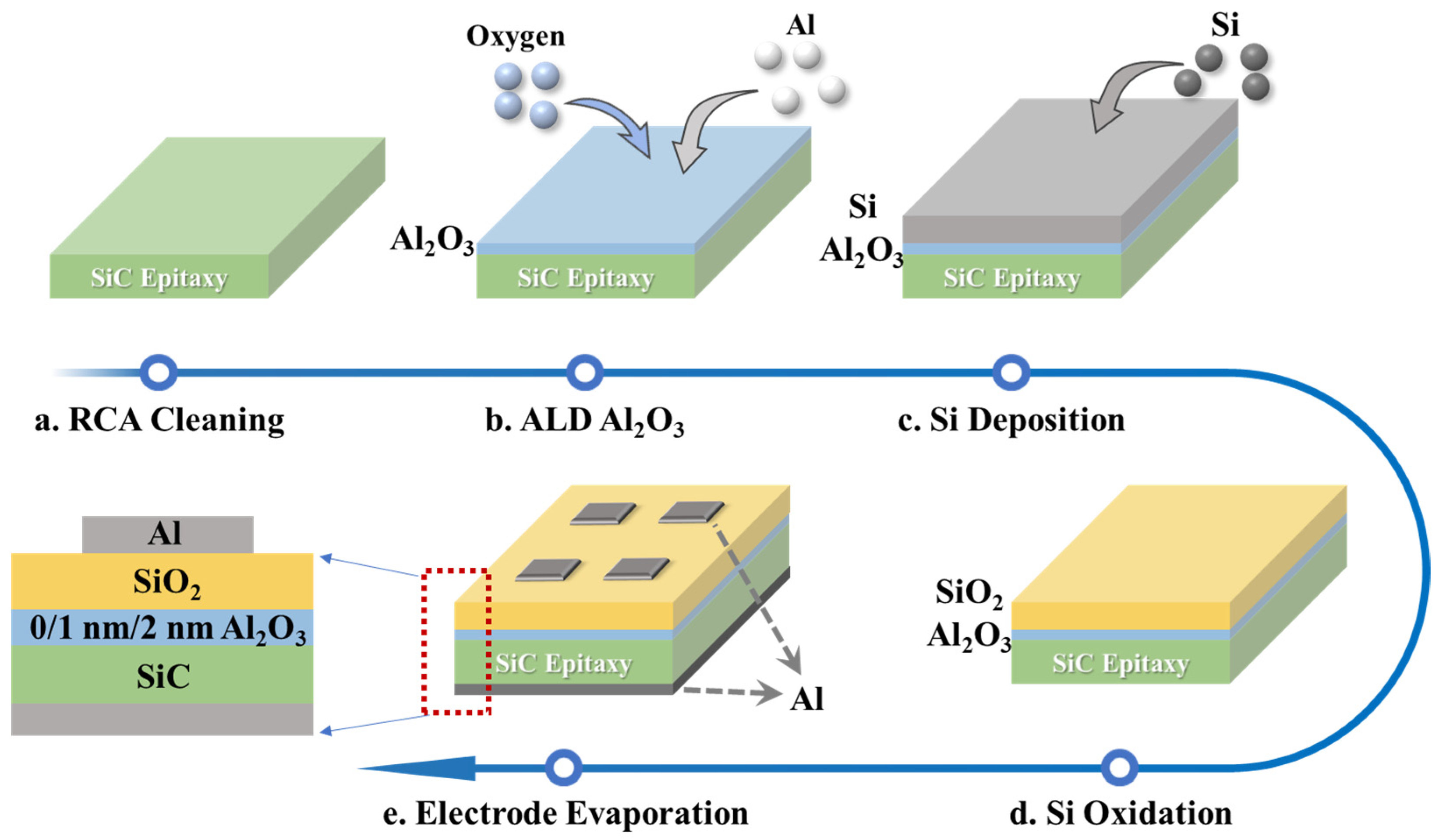
2.1. Fabrication of SiC MOS Capacitors

The substrates were n-type 4H-SiC (0001). The epitaxial layer had a doping concentration equal to 1 × 1016 cm−3 and a thickness of 5 μm. As shown in Figure 1, the experimental procedure was as follows:
(a)
The SiC epitaxial wafers were subjected to RCA cleaning to remove surface impurities, ensuring that the wafer surface was clean for the smooth progression of subsequent processes.
(b)
Al2O3 was deposited on the epitaxial wafer surface using ALD technology with 10 and 20 cycles, while a sample without Al2O3 deposition was prepared as a control group.
(c)
A 20 nm thick Si layer was grown on the prepared three groups of samples in a conventional plasma-enhanced chemical vapor deposition (PECVD) system. The Si film was deposited using SiH4 gas highly diluted with H4. The PECVD system operated at a radio frequency of 13.56 MHz, a substrate temperature of 250 °C, and an r.f. power of 50 W.
(d)
The samples underwent wet oxidation at 1100 °C for 2 h, during which the PECVD-grown silicon films were fully oxidized into SiO2 layers, with consistent silicon growth and thermal oxidation conditions maintained across all samples to ensure experimental uniformity. The samples were classified as follows: SiO2/SiC-A sample without Al2O3 deposition; SiO2/1 nm-Al2O3/SiC-A sample with 10 cycles of Al2O3 passivation layers; SiO2/2 nm-Al2O3/SiC-A sample with 20 cycles of Al2O3 passivation layers.
(e)
After coating a layer of photoresist on the front side of the sample, hydrofluoric acid was used to remove the excess SiO2 from the back side of the samples. The photoresist was then removed, and square electrodes, 200 μm in width and 200 nm in thickness, were deposited on the front side using electron beam evaporation. Additionally, a 200 μm thick aluminum electrode was also deposited on the back side of the sample.

2.2. Characterization

The samples’ surface roughness (Rq) and morphology were examined using a Bruker BRK0003 atomic force microscope (AFM) over areas of the sample measuring 5 × 5 μm2. Multiple measurements (n = 10) were performed on different areas of each sample, and the most reliable roughness values were determined through statistical analysis for data presentation. The surface chemical states were analyzed using an Escalab 250Xi XPS system from Thermo Scientific equipped with a monochromatic Al-Kα X-ray source at 1486.6 eV and a power of 150 W. Before the XPS analysis, the SiO2 film on the SiC epitaxy was etched to a thickness of approximately 5 nm using a 1% HF buffered solution.
The electrical properties of the SiC/SiO2 capacitors were characterized using a TS2000-HP probe station and a Keithley 4200A-S semiconductor analyzer. The insulation and breakdown characteristics of the oxide layer were evaluated by recording the current–voltage (IV) curves at room temperature. The Dit was extracted using the high–low frequency method within an energy range 0.2–0.6 eV below the conduction band edge. The CV curves were measured at 300 K using high-frequency (1 MHz) and quasi-static methods. The voltage stabilities were evaluated utilizing Vfb hysteresis after alternate positive bias stress (PBS) and negative bias stress (NBS) at different temperatures (300, 350, 400, and 450 K). The CV curves were swept from +20 to −20 V after the PBS (+2.5 MV cm−1) for 600 s. Following the same procedure, the CV curves were swept from −20 to +20 V after the NBS (−2.5 MV cm−1) for 600 s. The Vfb/midgap voltage (Vmg) hysteresis was obtained from the shift between Vfb and Vmg after PBS and NBS.

3. Results and Discussion

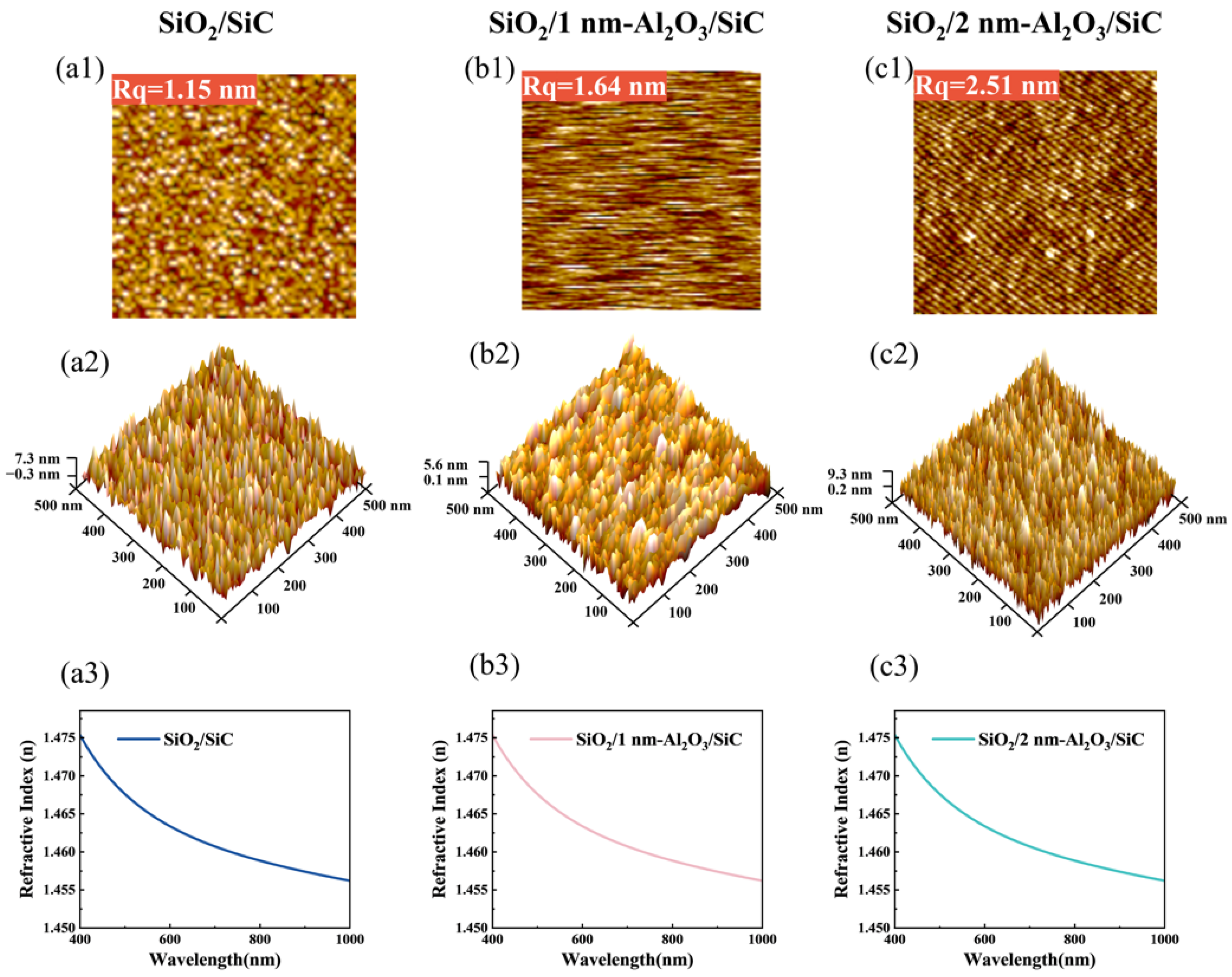
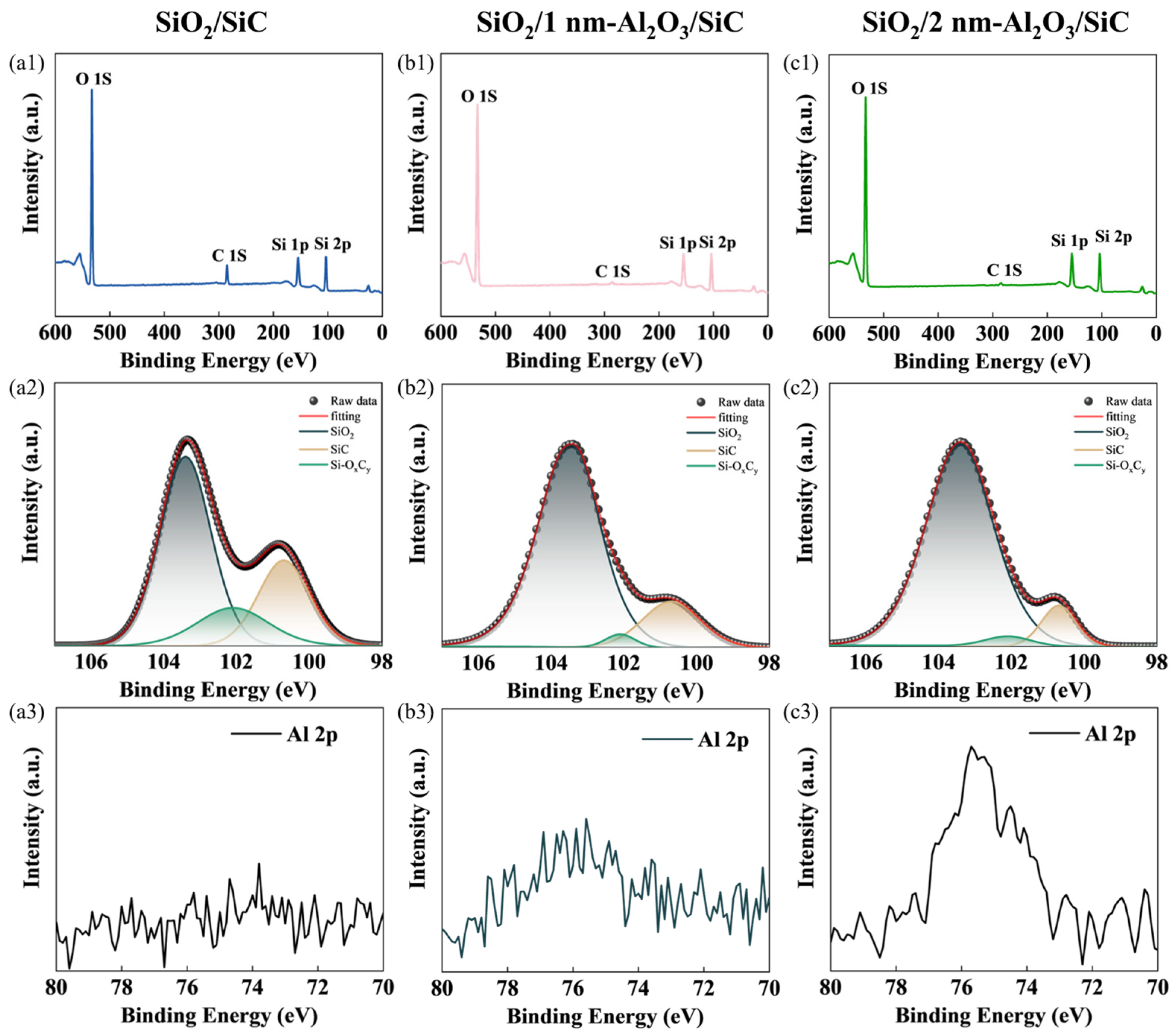
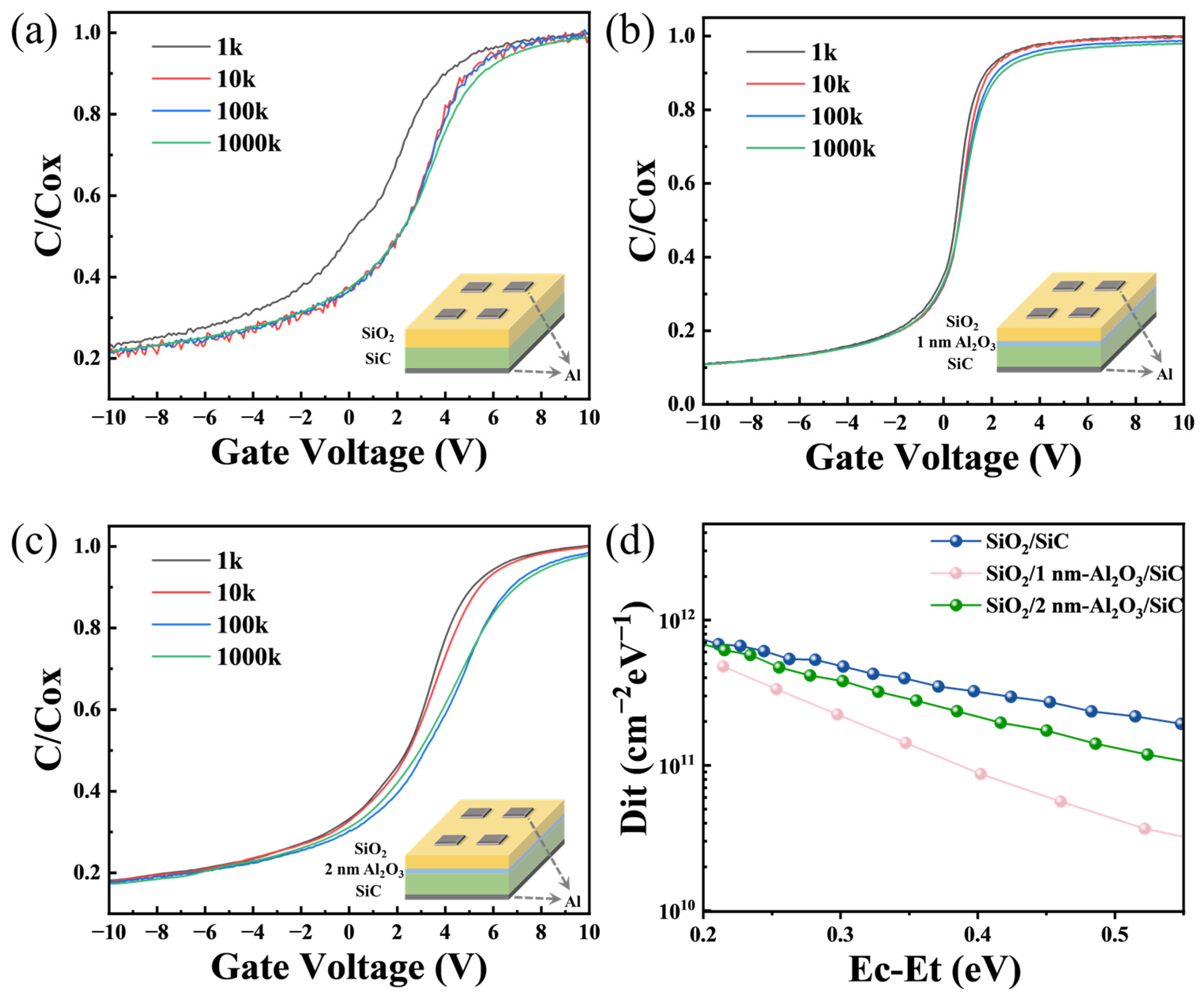
3.1. Interfacial Qualities and Characteristics of the SiO2 Films

The surface roughness of the MOS capacitor was characterized using AFM with a scanning area of 5 × 5 μm2. The AFM topographic image was shown in Figure 2, and the root mean square roughness values of the gate dielectric surface were calculated to be 1.15 nm, 1.64 nm, and 2.51 nm, respectively. When the passivation cycle reaches 10 times, the surface roughness of the SiO2 layer slightly increases to 1.64 nm compared to the control sample. It is noteworthy that the surface roughness increases significantly to 2.51 nm as the passivation interlayer thickens. This increase in roughness can be attributed to the additional ALD process step, which introduces more interfaces and potentially creates more surface irregularities during the fabrication process. However, this increase in surface roughness does not negatively impact the passivation effectiveness of the Al2O3 interlayer, as evidenced by our subsequent electrical measurements, which demonstrate that the samples with an Al2O3 passivation layer exhibit lower interface defect density and wider barrier height.
XPS was used to analyze the chemical bonds at the SiO2/SiC interface. The C 1s peak, attributed to adventitious carbon, is typically fixed at approximately 284.8 eV upon calibration of the measurements using a charge neutralizer.
Figure 3 compares the XPS results of the SiC/SiO2 interface with different Al2O3 passivation layers. Two weak Al 2p peaks were detected in both Figure 3(b3,c3) compared to Figure 3(a3). The peak in SiO2/1 nm-Al2O3/SiC with 10 ALD growth cycles in Figure 3(b3) is slightly weaker, while the peak in SiO2/2 nm-Al2O3/SiC with 20 ALD growth cycles in Figure 3(c3) is slightly stronger.
In the Si 2p spectrum, the binding energies are 100.7, 101.7, and 103.1 eV, corresponding to Si–C, Si–OxCy, and Si–O bonds, respectively [32,33,34]. The Si 2p spectrum shows a decrease in the SiOxCy components after the passivation layer was added, as shown in Figure 3(b2,c2). These observations indicate that it is unrealistic to prevent oxidation of the SiC substrate solely by temperature control, as low-temperature oxidation may still introduce some issues to the interface properties. However, an appropriate Al2O3 passivation cycle can effectively suppress defect formation.
As shown in Figure 4, to study the effect of different passivation growth cycles on the capacitance parameters of SiC/SiO2 capacitors, the CV characteristics were measured in the frequency range from 1 kHz to 1 MHz. The experiment revealed that each sample exhibited varying degrees of frequency dispersion. Adding 10 cycles of Al2O3 passivation layer helps to suppress the generation of interface defects, allowing most carriers to accumulate effectively on the semiconductor surface, thereby improving the dielectric performance of the SiC MOS capacitors. When the passivation cycle reaches 20c, SiO2/2 nm-Al2O3/SiC exhibits significant frequency dispersion. To quantitatively analyze the impact of different passivation layer thicknesses on the SiO2/SiC interface characteristics, we extracted the values of Dit for each sample, as shown in Figure 4d. The results indicate that around EcEt ≈ 0.3 eV, the Dit values for the three samples are approximately: 5 × 10¹¹, 2 × 10¹¹, and 4 × 1011 cm−2 eV−1, respectively. Compared to the structure without a passivation layer, the Dit at various energy levels is reduced after adding the Al2O3 passivation layer, especially around the trap energy level of approximately 0.6 eV, where a more significant reduction in Dit is observed. This demonstrates that the addition of the passivation layer effectively reduces the interface state density, thereby improving the quality of the interface, with the SiO2/1 nm-Al2O3/SiC structure exhibiting lower Dit values than the SiO2/SiC structure; moreover, compared to the previously reported Al2O3/SiC structures [35], our composite structure also achieves a significant reduction in Dit values, further confirming the effectiveness of this passivation approach.
However, in the MOS structure with the Al2O3 passivation layer, the Dit value for SiO2/2 nm-Al2O3/SiC configuration is obser ved to be higher than that for the SiO2/1 nm-Al2O3/SiC configuration. This deterioration in interface quality with increasing Al2O3 thickness (from 1 nm to 2 nm) can be attributed to the underlying mechanisms governing interface formation. As reported by Boan et al. [26], when gate materials are directly deposited on SiC using ALD techniques, the resulting interface typically exhibits significantly higher Dit values compared to thermally grown oxides. Their research revealed that Al2O3/SiC interfaces formed through direct deposition generally exhibit poor interface quality. To address this issue, researchers have developed two main approaches: (1) Applying post-deposition annealing treatments to improve the electrical properties of the ALD-deposited dielectric layer and its interface with SiC [36,37]; (2) Adopting a multilayer structure where SiC is first thermally oxidized to form a SiO2 layer before depositing high-K materials (such as HfO2/Al2O3) on top, creating a high-K material/thermally oxidized SiO2/SiC stack that significantly reduces interface trap densities [27,38]. Based on these findings, we propose that as the Al2O3 layer thickness increases from 1 nm to 2 nm, its functional role shifts from primarily acting as a passivation layer to resembling a directly ALD-deposited gate oxide in direct contact with SiC. At 1 nm thickness, the Al2O3 layer effectively passivates interface traps while preserving the advantageous properties of the underlying thermally grown SiO2/SiC interface. However, at 2 nm thickness, the Al2O3 layer begins to dominate the interface characteristics, leading to properties that closely resemble those of direct ALD-deposited Al2O3/SiC structures, which inherently exhibit higher Dit values. This thickness-dependent transition in interface behavior accounts for the observed increase in Dit values despite the increased physical thickness of the passivation layer. Consequently, the careful optimization of the Al2O3 passivation layer thickness is crucial to prevent the Al2O3 layer from transitioning from a passivation effect to a layered structure.
To study the effect of the Al2O3 passivation layer on the insulating properties of the SiO2 film, we performed IV measurements. The current density–electric field (JE) curves of the SiC MOS capacitors were shown in Figure 5. Compared to the SiO2/SiC sample, the SiO2/1 nm-Al2O3/SiC and SiO2/2 nm-Al2O3/SiC exhibit lower leakage currents, with the Ebd increasing to 10.9 MV/cm, 9.94 MV/cm, respectively. All three samples show typical Fowler–Nordheim (FN) tunneling characteristics. The expression for FN tunneling is as follows [39]:
J = q 3 E 2 16 π 2 φ o x exp 4 2 m T * φ B 3 / 2 3 q E
where q is the elementary charge, m T * is the effective mass of the electrons in the SiO2 film, and is the reduced Planck constant. By calculating the JE data for the three samples, the results are shown in Table 1. We calculated the effective electron barrier heights for SiO2/SiC, SiO2/1 nm-Al2O3/SiC, and SiO2/2 nm-Al2O3/SiC, which are 2.15 eV, 2.51 eV, and 2.37 eV, respectively. Therefore, it can be concluded that the passivation layer effectively prevents the diffusion of harmful chemical species during the oxidation process of SiC, as previously reported in previous studies [29]. This helps improve the insulating properties of the SiO2 film and contributes to a more stable and improved interface structure. This also explains why the conduction band offset of SiO2/1 nm-Al2O3/SiC is closer to the theoretical value.

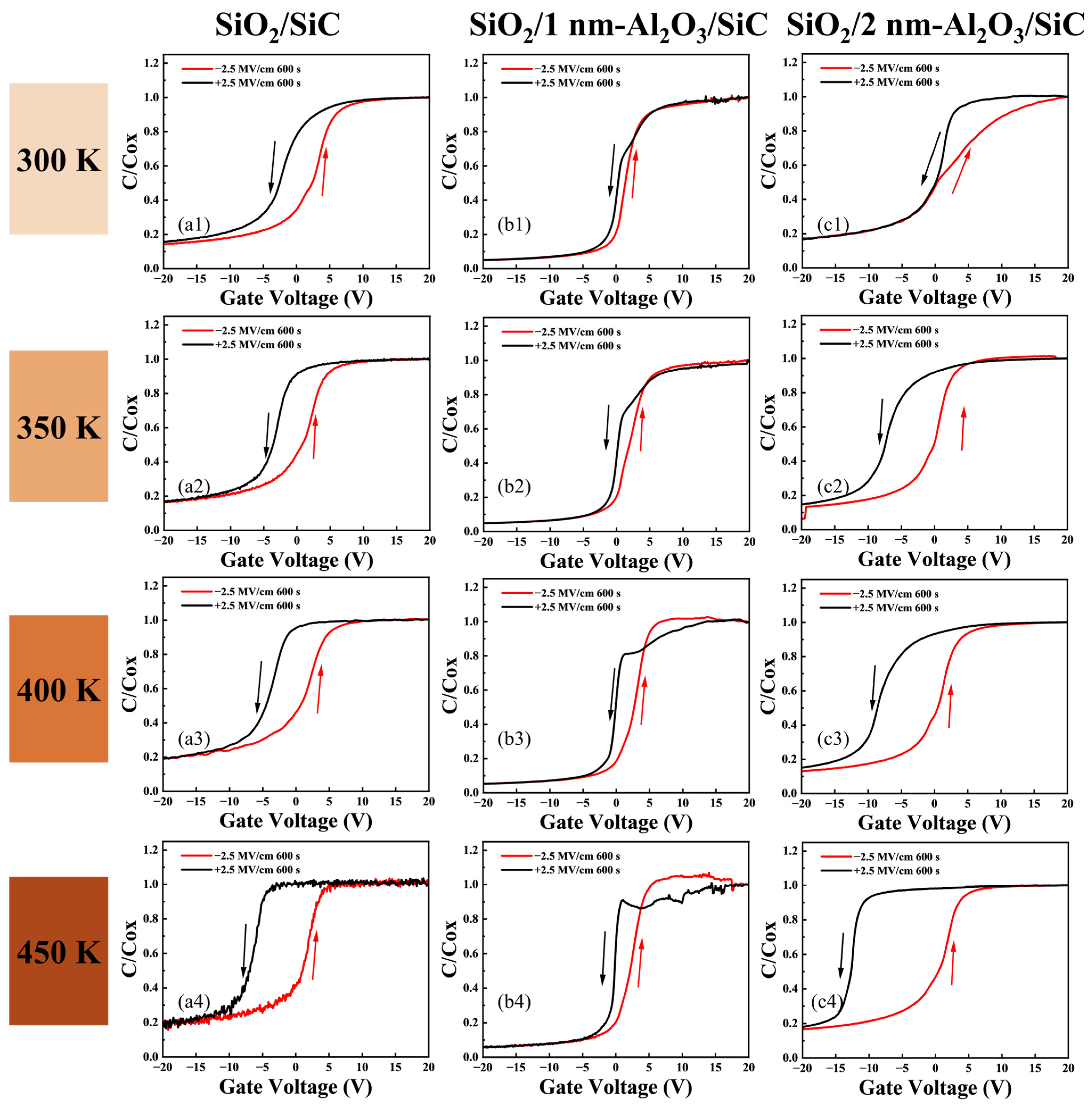
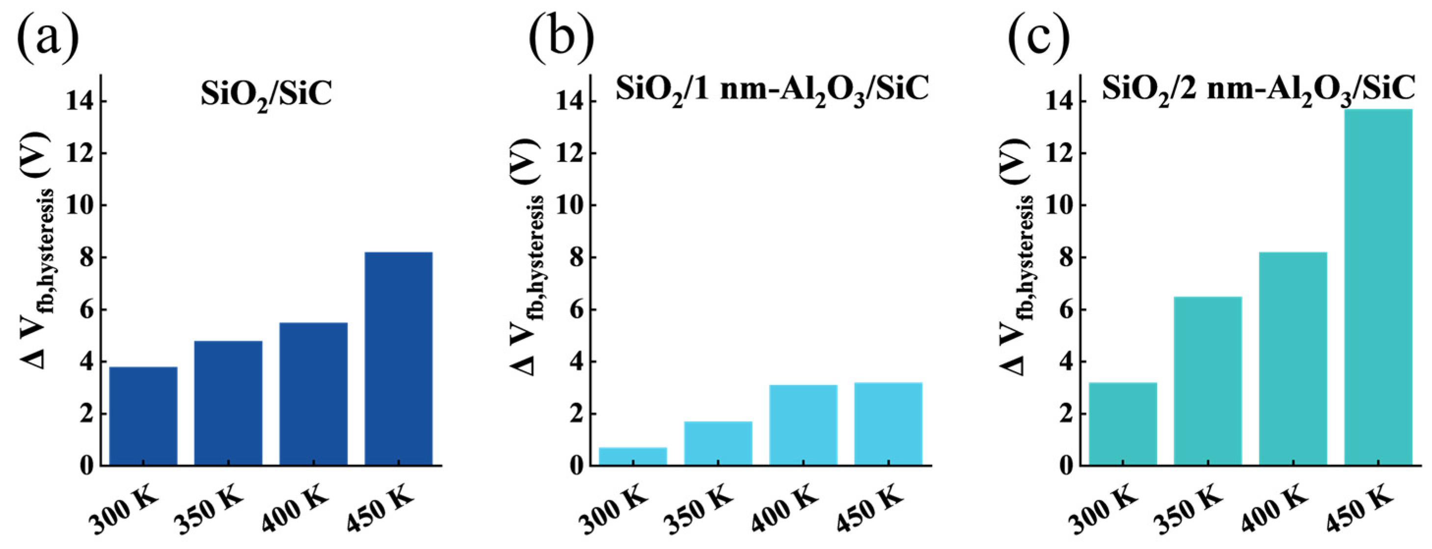
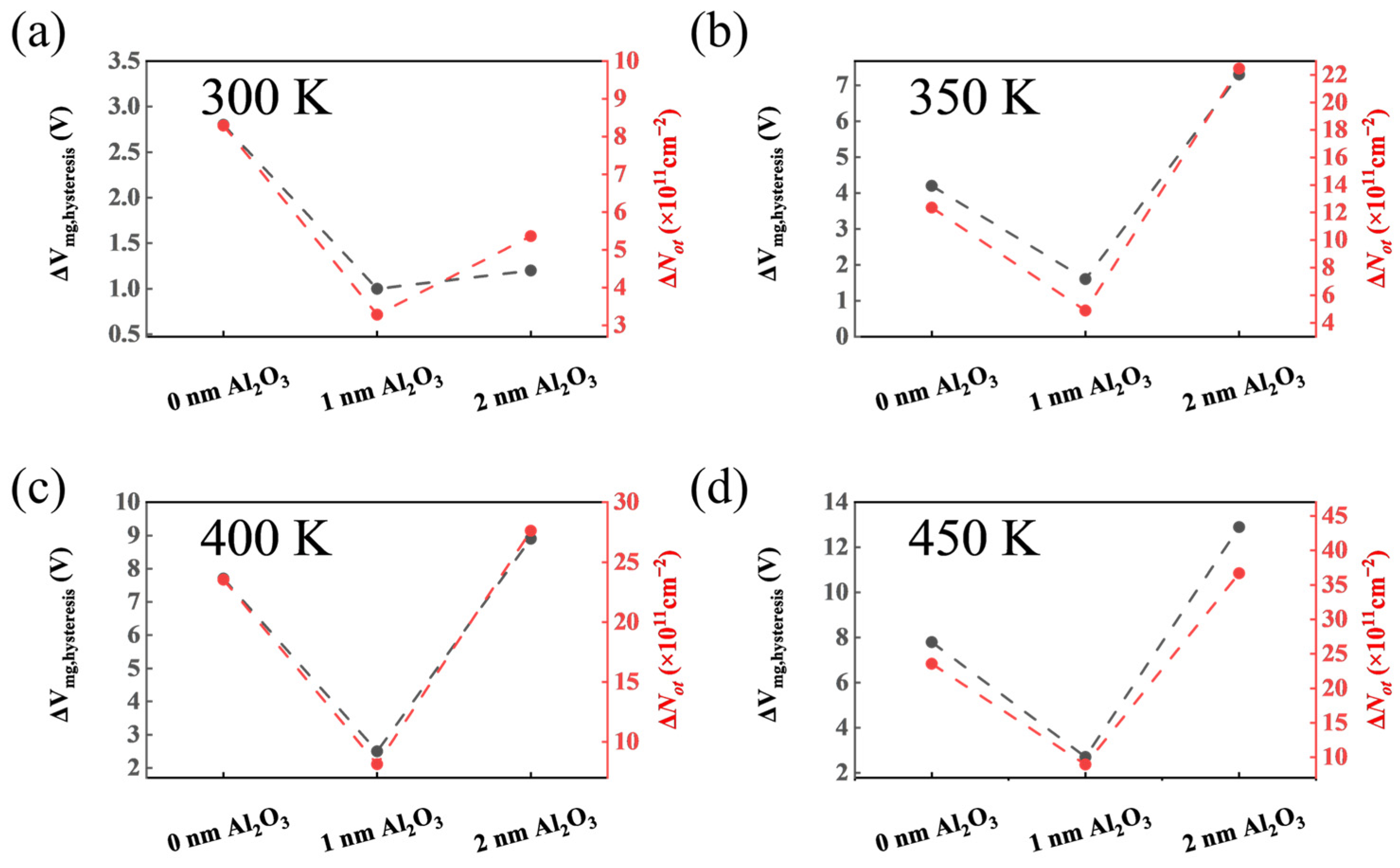
3.2. Thermal Stability of SiC MOS Capacitors

In SiC MOS devices, the main sources of instability are typically considered to be the SiC/SiO2 interface and its near interface charge trapping, as well as the mobile ions in the gate oxide [40,41]. As shown in Figure 6, all the high-frequency (HF) CV curves exhibit a counterclockwise hysteresis, indicating that the impact of trap charge trapping on the CV drift in the samples is smaller than the effect of mobile ions [33].
We also studied the changes in ΔVfb and ΔVmg hysteresis under alternating PBTS and NBTS at temperatures of 300 K, 350 K, 400 K, and 450 K for samples with passivation layer thicknesses. As shown in Figure 7 and Figure 8, ΔVfb and ΔVmg were extracted using midgap capacitance and flat-band capacitance as reference points. It was observed that in all three samples, the HF CV curve hysteresis of SiO2/1 nm-Al2O3/SiC was relatively small at different temperatures, which demonstrates that the Al2O3 passivation layer with ten cycles reduces the traps near the interface, thereby improving the stability of BTS. Combined with the Dit results, it can be inferred that the 10c Al2O3 layer effectively prevents low-temperature oxidation of SiC and reduces interface traps, thereby improving the interface quality and the Vfb stability of the SiC MOS capacitors. As the passivation cycle reaches 20c, the ΔVfb and ΔVmg of SiO2/2 nm-Al2O3/SiC significantly increase. This increased hysteresis behavior indicates that the excessive Al2O3 passivation layer induces additional activated traps under high-temperature stress.

4. Conclusions

In this study, a SiO2/4H-SiC gate dielectric with low interface state density and high stability was successfully fabricated. A novel process was employed, in which an ultra-thin passivation layer of Al2O3 was deposited on the SiC surface using ALD. The Al2O3 layer protected the SiC surface by preventing the diffusion of harmful chemical species during the oxidation process. Si was then deposited atop the Al2O3 layer and re-oxidized to form a high-quality gate oxide layer. We systematically investigated the influence of the Al2O3 passivation layer on interface properties and optimized the fabrication method. Compared to samples without the Al2O3 passivation layer, the SiO2/1 nm-Al2O3/SiC MOS capacitor demonstrated a significant reduction in Dit. Long-term high-temperature stability was assessed via flat-band voltage bias stress tests, revealing that the Al2O3 layer effectively suppressed the formation of near interface oxide traps and enhanced the stability of the oxide layer. This method offers a novel avenue for overcoming the performance bottlenecks of SiC MOSFETs.

Author Contributions

Methodology, Z.W.; Software, Z.W.; Data curation, Z.W. and Y.S.; Formal analysis, Z.W., Y.G. and C.D.; Writing—original draft, Z.W.; Validation, Z.B.; Investigation, Z.B., Y.G., Q.H., L.G. and Q.Z.; Project administration, Q.Z. and H.M.; Supervision, Q.Z. and H.M.; Resources, Q.Z.; Writing—review and editing, Q.Z. and H.M.; Conceptualization, H.M.; Funding acquisition, H.M. All authors have read and agreed to the published version of the manuscript.

Funding

This research is supported by the National Natural Science Foundation of China (Nos. 11804055, 11875204, and U1932167), Science and Technology Innovation Plan of Shanghai Science and Technology Commission (Nos. 21DZ1100800, 23ZR1405300, 20501110700, and 20501110702).

Data Availability Statement

The data that support the findings of this study are available from the corresponding author, Hong-Ping Ma, upon reasonable request.

Conflicts of Interest

The authors declare that they have no known competing financial interests or personal relationships that could have appeared to influence the work reported in this paper.

References

  1. Baliga, B.J. Silicon carbide power devices: Progress and future outlook. IEEE J. Emerg. Sel. Top. Power Electron. 2023, 11, 2400–2411. [Google Scholar]
  2. Liu, G.; Tuttle, B.R.; Dhar, S. Silicon carbide: A unique platform for metal-oxide-semiconductor physics. Appl. Phys. Rev. 2015, 2, 021307. [Google Scholar] [CrossRef]
  3. Millan, J.; Godignon, P.; Perpiñà, X.; Pérez-Tomás, A.; Rebollo, J. A survey of wide bandgap power semiconductor devices. IEEE Trans. Power Electron. 2013, 29, 2155–2163. [Google Scholar]
  4. Lipkin, L.; Palmour, J. Improved oxidation procedures for reduced SiO2/SiC defects. J. Electron. Mater. 1996, 25, 909–915. [Google Scholar]
  5. Roy, J.; Chandra, S.; Das, S.; Maitra, S. Oxidation behaviour of silicon carbide—A review. Rev. Adv. Mater. Sci. 2014, 38, 29–39. [Google Scholar]
  6. Wang, Y.; Ding, Y.; Yin, Y. Reliability of wide band gap power electronic semiconductor and packaging: A review. Energies 2022, 15, 6670. [Google Scholar] [CrossRef]
  7. Cabello, M.; Soler, V.; Rius, G.; Montserrat, J.; Rebollo, J.; Godignon, P. Advanced processing for mobility improvement in 4H-SiC MOSFETs: A review. Mater. Sci. Semicond. Process. 2018, 78, 22–31. [Google Scholar]
  8. Pande, P.; Haasmann, D.; Han, J.; Moghadam, H.A.; Tanner, P.; Dimitrijev, S. Electrical characterization of SiC MOS capacitors: A critical review. Microelectron. Reliab. 2020, 112, 113790. [Google Scholar] [CrossRef]
  9. Buffolo, M.; Favero, D.; Marcuzzi, A.; De Santi, C.; Meneghesso, G.; Zanoni, E.; Meneghini, M. Review and outlook on GaN and SiC power devices: Industrial state-of-the-art, applications, and perspectives. IEEE Trans. Electron Devices 2024, 71, 1344–1355. [Google Scholar]
  10. Zhang, Q.; You, N.; Liu, P.; Wang, J.; Xu, Y.; Wang, S. Study of defects distribution in SiO2/SiC with plasma oxidation and post oxidation annealing. Appl. Surf. Sci. 2023, 610, 155500. [Google Scholar]
  11. Zhang, Q.; You, N.; Wang, J.; Xu, Y.; Zhang, K.; Wang, S. Effect of Temperature-Dependent Low Oxygen Partial Pressure Annealing on SiC MOS. Nanomaterials 2024, 14, 192. [Google Scholar] [CrossRef] [PubMed]
  12. Sharma, Y.; Ahyi, A.; Issacs-Smith, T.; Shen, X.; Pantelides, S.; Zhu, X.; Feldman, L.; Rozen, J.; Williams, J. Phosphorous passivation of the SiO2/4H–SiC interface Solid-State. Electronics 2012, 68, 103–107. [Google Scholar]
  13. Okamoto, D.; Sometani, M.; Harada, S.; Kosugi, R.; Yonezawa, Y.; Yano, H. Improved channel mobility in 4H-SiC MOSFETs by boron passivation. IEEE Electron Device Lett. 2014, 35, 1176–1178. [Google Scholar] [CrossRef]
  14. Wang, R.; Noguchi, M.; Watanabe, H.; Kita, K. Dependence of the incorporated boron concentration near SiO2/4H–SiC interface on trap passivation reduction. AIP Adv. 2024, 14, 075304. [Google Scholar] [CrossRef]
  15. Okamoto, D.; Sometani, M.; Harada, S.; Kosugi, R.; Yonezawa, Y.; Yano, H. Effect of boron incorporation on slow interface traps in SiO2/4H-SiC structures. Appl. Phys. A 2017, 123, 133. [Google Scholar] [CrossRef]
  16. Zheng, Y.; Isaacs-Smith, T.; Ahyi, A.; Dhar, S. 4H-SiC MOSFETs with borosilicate glass gate dielectric and antimony counter-doping. IEEE Electron Device Lett. 2017, 38, 1433–1436. [Google Scholar] [CrossRef]
  17. Jia, Y.; Lv, H.; Tang, X.; Han, C.; Song, Q.; Zhang, Y.; Zhang, Y.; Dimitrijev, S.; Han, J. Growth and characterization of nitrogen-phosphorus hybrid passivated gate oxide film on N-type 4H-SiC epilayer. J. Cryst. Growth 2019, 507, 98–102. [Google Scholar] [CrossRef]
  18. Kobayashi, T.; Okuda, T.; Tachiki, K.; Ito, K.; Matsushita, Y.-I.; Kimoto, T. Design and formation of SiC (0001)/SiO2 interfaces via Si deposition followed by low-temperature oxidation and high-temperature nitridation. Appl. Phys. Express 2020, 13, 091003. [Google Scholar] [CrossRef]
  19. Li, Y.; Zhao, S.; Wei, M.; Jiao, J.; Yan, G.; Liu, X. Preparation and oxidation characteristics of Si layers grown on 4H–SiC substrates. Vacuum 2024, 227, 113418. [Google Scholar] [CrossRef]
  20. Nigro, R.L.; Fiorenza, P.; Greco, G.; Schilirò, E.; Roccaforte, F. Structural and insulating behaviour of high-permittivity binary oxide thin films for silicon carbide and gallium nitride electronic devices. Materials 2022, 15, 830. [Google Scholar] [CrossRef]
  21. Siddiqui, A.; Khosa, R.Y.; Usman, M. High-k dielectrics for 4H-silicon carbide: Present status and future perspectives. J. Mater. Chem. C 2021, 9, 5055–5081. [Google Scholar] [CrossRef]
  22. Wirths, S.; Arango, Y.; Mihaila, A.; Bellini, M.; Romano, G.; Alfieri, G.; Belanche, M.; Knoll, L.; Bianda, E.; Mengotti, E. Vertical power SiC MOSFETs with high-k gate dielectrics and superior threshold voltage stability. In Proceedings of the 2020 32nd International Symposium on Power Semiconductor Devices and ICs (ISPSD), IEEE, Vienna, Austria, 13–18 September 2020; pp. 226–229. [Google Scholar]
  23. Chang, P.; Hwu, J. Electrical characterization of 4H-SiC metal–oxide–semiconductor structure with Al2O3 stacking layers as dielectric. Appl. Phys. A 2018, 124, 87. [Google Scholar] [CrossRef]
  24. Khosa, R.Y.; Thorsteinsson, E.; Winters, M.; Rorsman, N.; Karhu, R.; Hassan, J.; Sveinbjörnsson, E. Electrical characterization of amorphous Al2O3 dielectric films on n-type 4H-SiC. Aip Adv. 2018, 8, 025304. [Google Scholar]
  25. Shukla, M.; Dutta, G.; Mannam, R.; DasGupta, N. Electrical properties of reactive-ion-sputtered Al2O3 on 4H-SiC. Thin Solid Film. 2016, 607, 1–6. [Google Scholar]
  26. Qin, B.; Liu, S.; You, N.; Liu, J.; Li, X.; Wang, S.; Li, X. Lowering of interface state density between deposited gate oxide and SiC substrate via controlling substrate oxidation. Vacuum 2024, 222, 112999. [Google Scholar]
  27. Schilirò, E.; Fiorenza, P.; Di Franco, S.; Bongiorno, C.; Saggio, M.; Roccaforte, F.; Nigro, R.L. Effect of SiO2 interlayer on the properties of Al2O3 thin films grown by plasma enhanced atomic layer deposition on 4H-SiC substrates. Phys. Status Solidi (a) 2017, 214, 1600365. [Google Scholar] [CrossRef]
  28. Chen, X.; Ge, L.; Cheong, K.Y.; Han, J.; Phan, H.-P.; Xu, M. Performance improvement of silicon carbide gate oxide interface by pre-oxidation. Appl. Surf. Sci. 2025, 688, 162359. [Google Scholar]
  29. Corrêa, S.A.; Marmitt, G.G.; Bom, N.M.; Da Rosa, A.; Stedile, F.C.; Radtke, C.; Soares, G.V.; Baumvol, I.J.R.; Krug, C.; Gobbi, A.L. Enhancement in interface robustness regarding thermal oxidation in nanostructured Al2O3 deposited on 4H-SiC. Appl. Phys. Lett. 2009, 95, 051916. [Google Scholar]
  30. Lu, J.; He, G.; Wang, W.; Jiang, S.; Wu, Q.; Fang, Z. Interface chemistry and defect state optimization of the ErSmO/InP heterojunction modified by ALD-driven Al2O3 interlayers. ACS Appl. Electron. Mater. 2023, 5, 935–947. [Google Scholar] [CrossRef]
  31. Shao, Z.; Xu, H.; Wang, H.; Ren, N.; Sheng, K. Saturation thickness of stacked SiO2 in atomic-layer-deposited Al2O3 gate on 4H-SiC. Chin. Phys. B 2023, 32, 087106. [Google Scholar]
  32. Yin, Z.; Wei, S.; Bai, J.; Xie, W.; Qin, F.; Wang, D. SiC/SiO2 interface properties formed by low-temperature ozone re-oxidation annealing. Ceram. Int. 2022, 48, 10874–10884. [Google Scholar]
  33. Wei, S.; Bai, J.; Xie, W.; Su, Y.; Qin, F.; Wang, D. Reliability and stability improvement of MOS capacitors via nitrogen–hydrogen mixed plasma pretreatment for SiC surfaces. ACS Appl. Mater. Interfaces 2023, 15, 18537–18549. [Google Scholar] [PubMed]
  34. Yang, C.; Yin, Z.; Zhang, F.; Su, Y.; Qin, F.; Wang, D. Synergistic passivation effects of nitrogen plasma and oxygen plasma on improving the interface quality and bias temperature instability of 4H-SiC MOS capacitors. Appl. Surf. Sci. 2020, 513, 145837. [Google Scholar]
  35. Guo, Y.-D.; Wang, A.-F.; Huang, Q.-M.; Wang, Z.-Y.; Ma, H.-P.; Zhang, Q. Performance Comparison of Al2O3 Gate Dielectric Grown on 4H-SiC Substrates via Thermal and Plasma-Enhanced Atomic Layer Deposition Methods. ECS J. Solid State Sci. Technol. 2025, 14, 023005. [Google Scholar]
  36. Lee, E.; Kim, T.H.; Lee, S.W.; Kim, J.H.; Kim, J.; Jeong, T.G.; Ahn, J.-H.; Cho, B. Improved electrical performance of a sol–gel IGZO transistor with high-k Al2O3 gate dielectric achieved by post annealing. Nano Converg. 2019, 6, 24. [Google Scholar]
  37. Nunomura, S.; Ota, H.; Irisawa, T.; Endo, K.; Morita, Y. Defect generation and recovery in high-k HfO2/SiO2/Si stack fabrication. Appl. Phys. Express 2023, 16, 061004. [Google Scholar]
  38. Kim, C.; Moon, J.H.; Yim, J.H.; Lee, D.H.; Lee, J.H.; Lee, H.H.; Kim, H.J. Comparison of thermal and atomic-layer-deposited oxides on 4H-SiC after post-oxidation-annealing in nitric oxide. Appl. Phys. Lett. 2012, 100, 082112. [Google Scholar]
  39. Chanana, R.K. Determination of hole effective mass in SiO2 and SiC conduction band offset using Fowler–Nordheim tunneling characteristics across metal-oxide-semiconductor structures after applying oxide field corrections. J. Appl. Phys. 2011, 109, 104508. [Google Scholar]
  40. Wang, Z.; Lin, Z.; Li, J.; Liu, W. Low-pressure oxidation for improving interface properties and voltage instability of SiO2/4H-SiC MOS capacitor. Appl. Surf. Sci. 2025, 681, 161604. [Google Scholar] [CrossRef]
  41. Chanthaphan, A.; Hosoi, T.; Mitani, S.; Nakano, Y.; Nakamura, T.; Shimura, T.; Watanabe, H. Investigation of unusual mobile ion effects in thermally grown SiO2 on 4H-SiC (0001) at high temperatures. Appl. Phys. Lett. 2012, 100, 252103. [Google Scholar]
Figure 1. Fabrication process flow of the SiC MOS capacitors.
Nanomaterials 15 00555 g001
Figure 2. Both 2D and 3D AFM images within the area of 5 × 5 μm2 for (a1,a2) SiO2/SiC, (b1,b2) SiO2/1 nm-Al2O3/SiC, and (c1,c2) SiO2/2 nm-Al2O3/SiC. SE results for (a3) SiO2/SiC, (b3) SiO2/1 nm-Al2O3/SiC, and (c3) SiO2/2 nm-Al2O3/SiC.
Nanomaterials 15 00555 g002
Figure 3. Acquired XPS survey spectrum for (a1) SiO2/SiC; (b1) SiO2/1 nm-Al2O3/SiC and (c1) SiO2/2 nm-Al2O3/SiC. Deconvolution of the Si 2p core levels for (a2) SiO2/SiC; (b2) SiO2/1 nm-Al2O3/SiC and (c2) SiO2/2 nm-Al2O3/SiC. Obtained XPS spectra of the Al 2p core levels for (a3) SiO2/SiC; (b3) SiO2/1 nm-Al2O3/SiC and (c3) SiO2/2 nm-Al2O3/SiC.
Nanomaterials 15 00555 g003
Figure 4. (a) Obtained CV curves for the SiO2/SiC at different test frequencies; (b) Obtained CV curves for the SiO2/1 nm-Al2O3/SiC at different test frequencies; (c) Obtained CV curves for the SiO2/2 nm-Al2O3/SiC at different test frequencies; (d) Distribution of Dit vs. energy level for SiO2/SiC, SiO2/1 nm-Al2O3/SiC, and SiO2/2 nm-Al2O3/SiC.
Nanomaterials 15 00555 g004
Figure 5. Room temperature JE curves for SiC MOS capacitors based on samples with different Al2O3 growth cycles.
Nanomaterials 15 00555 g005
Figure 6. High-frequency CV curves for SiC MOS capacitors after alternate PBS (2.5 MV cm−1, 600 s) and NBS (−2.5 MV cm−1, 600 s) for different samples at various temperatures, including SiO2/SiC at (a1) 300 K; (a2) 350 K; (a3) 400 K and (a4) 450 K; SiO2/1 nm-Al2O3/SiC at (b1) 300 K; (b2) 350 K; (b3) 400 K and (b4) 450 K and SiO2/2 nm-Al2O3/SiC at (c1) 300 K; (c2) 350 K; (c3) 400 K and (c4) 450 K.
Nanomaterials 15 00555 g006
Figure 7. Vfb hysteresis in the high-frequency CV curves for SiC MOS capacitors after alternate PBS (2.5 MV cm−1, 600 s) and NBS (−2.5 MV cm−1, 600 s) at temperatures ranging from 300 to 450 K for samples (a) SiO2/SiC; (b) SiO2/1 nm-Al2O3/SiC, and (c) SiO2/2 nm-Al2O3/SiC.
Nanomaterials 15 00555 g007
Figure 8. ΔVmg hysteresis in the high-frequency CV curves and areal density of ΔNot in the SiC MOS capacitors after alternate PBS (2.5 MV cm−1, 600 s) and NBS (−2.5 MV cm−1, 600 s) at (a) 300 K; (b) 350 K; (c) 400 K and (d) 450 K.
Nanomaterials 15 00555 g008
Table 1. Comparison of barrier height and breakdown field for the three 4H-SiC MOS structures.
Theoretical [28]SiO2/SiCSiO2/1 nm-Al2O3/SiCSiO2/2 nm-Al2O3/SiC
φB (eV) @25 °C2.72.152.512.37
Ebd (MV cm−1)109.6410.99.94
Disclaimer/Publisher’s Note: The statements, opinions and data contained in all publications are solely those of the individual author(s) and contributor(s) and not of MDPI and/or the editor(s). MDPI and/or the editor(s) disclaim responsibility for any injury to people or property resulting from any ideas, methods, instructions or products referred to in the content.

