
Versatile Approach of Silicon Nanofabrication without Resists: Helium Ion-Bombardment Enhanced Etching


Abstract
1. Introduction
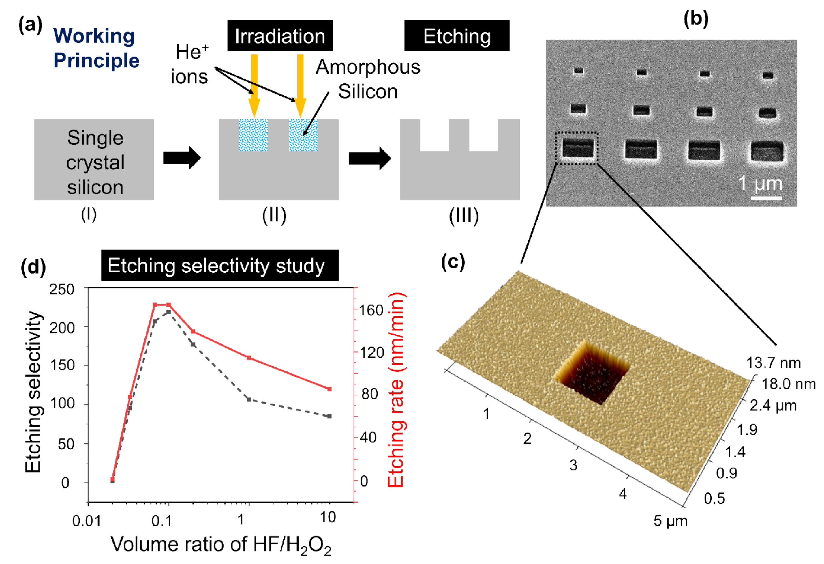
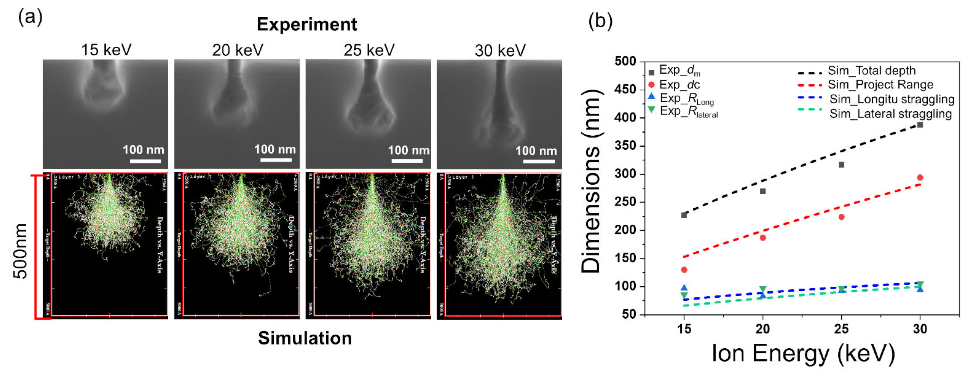
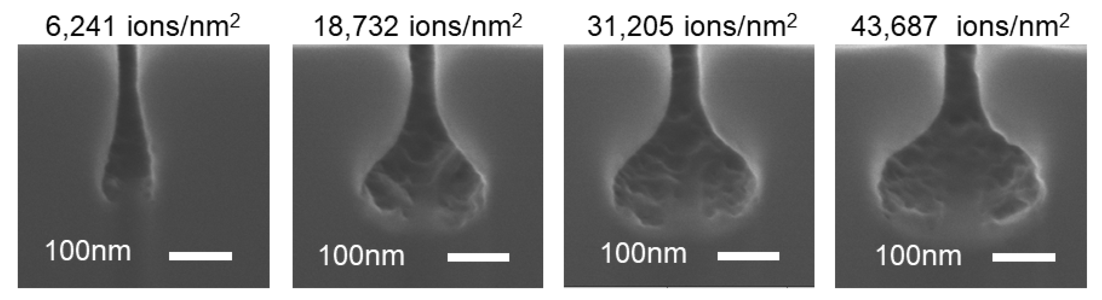
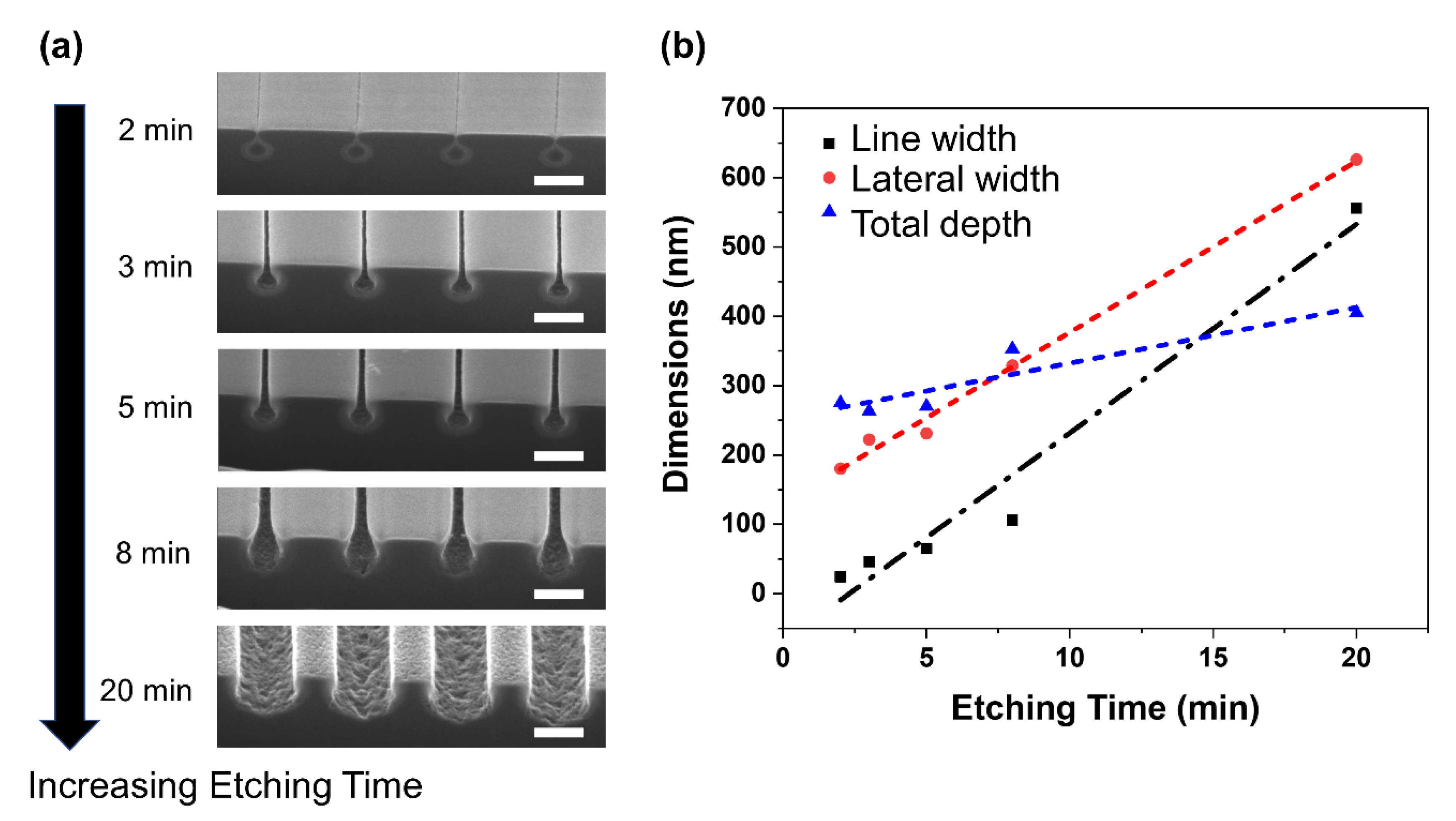
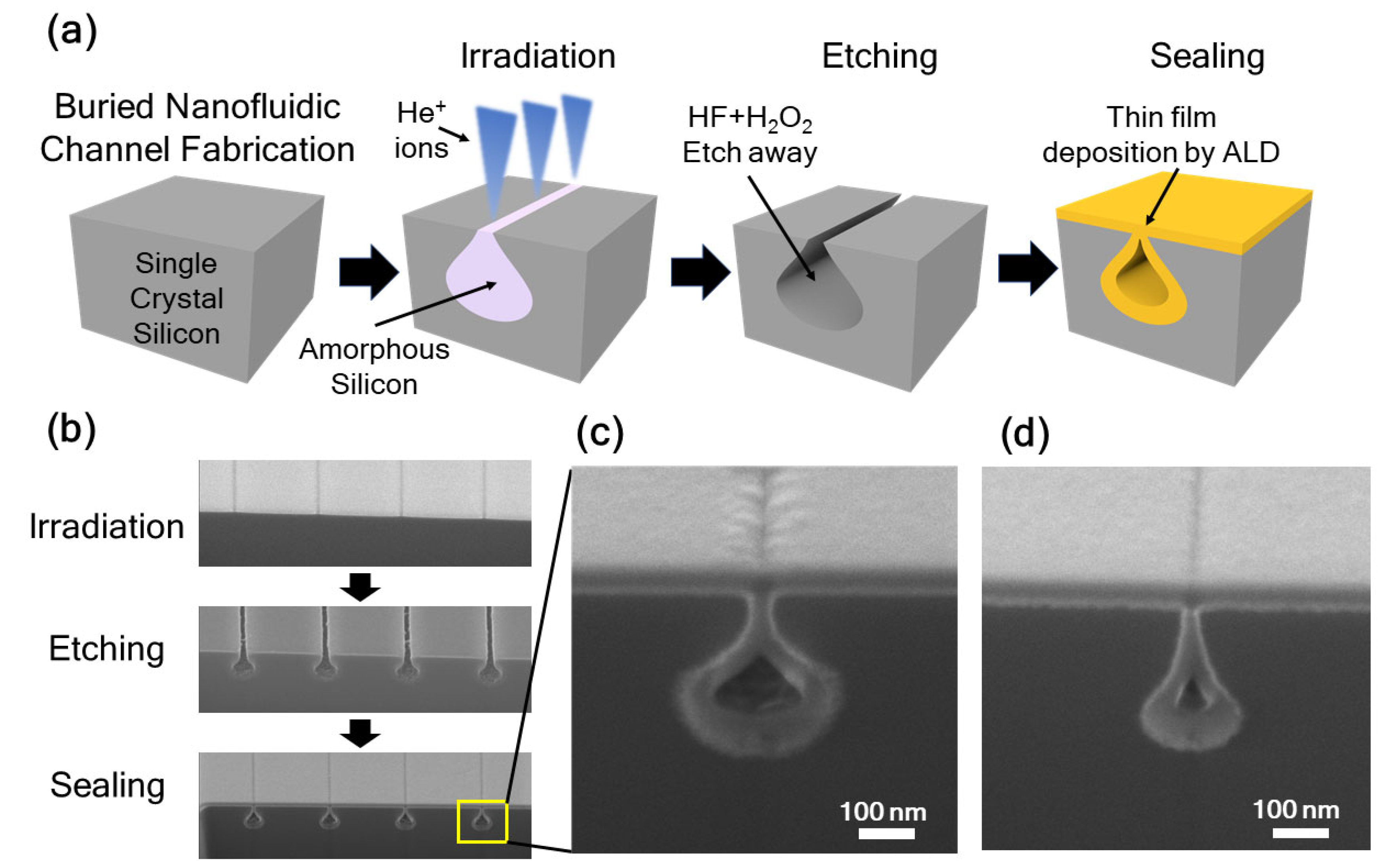
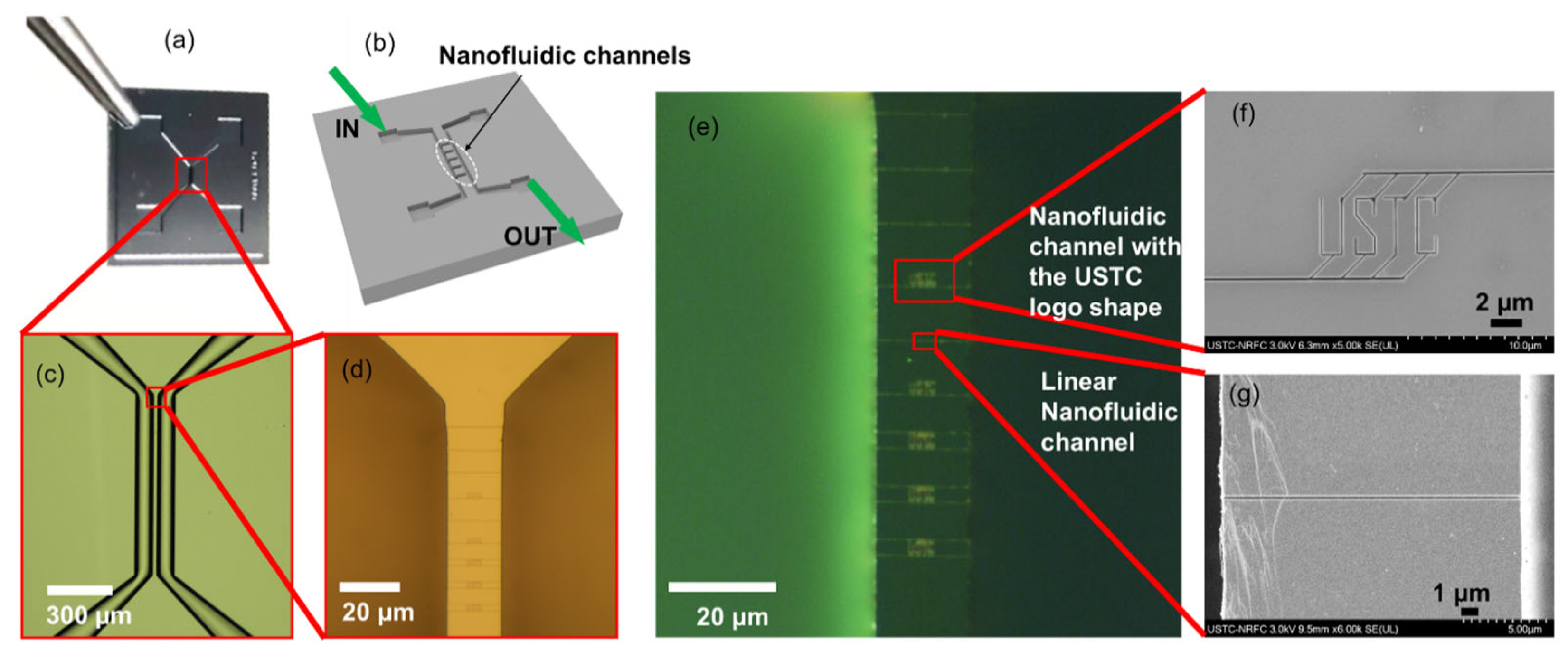
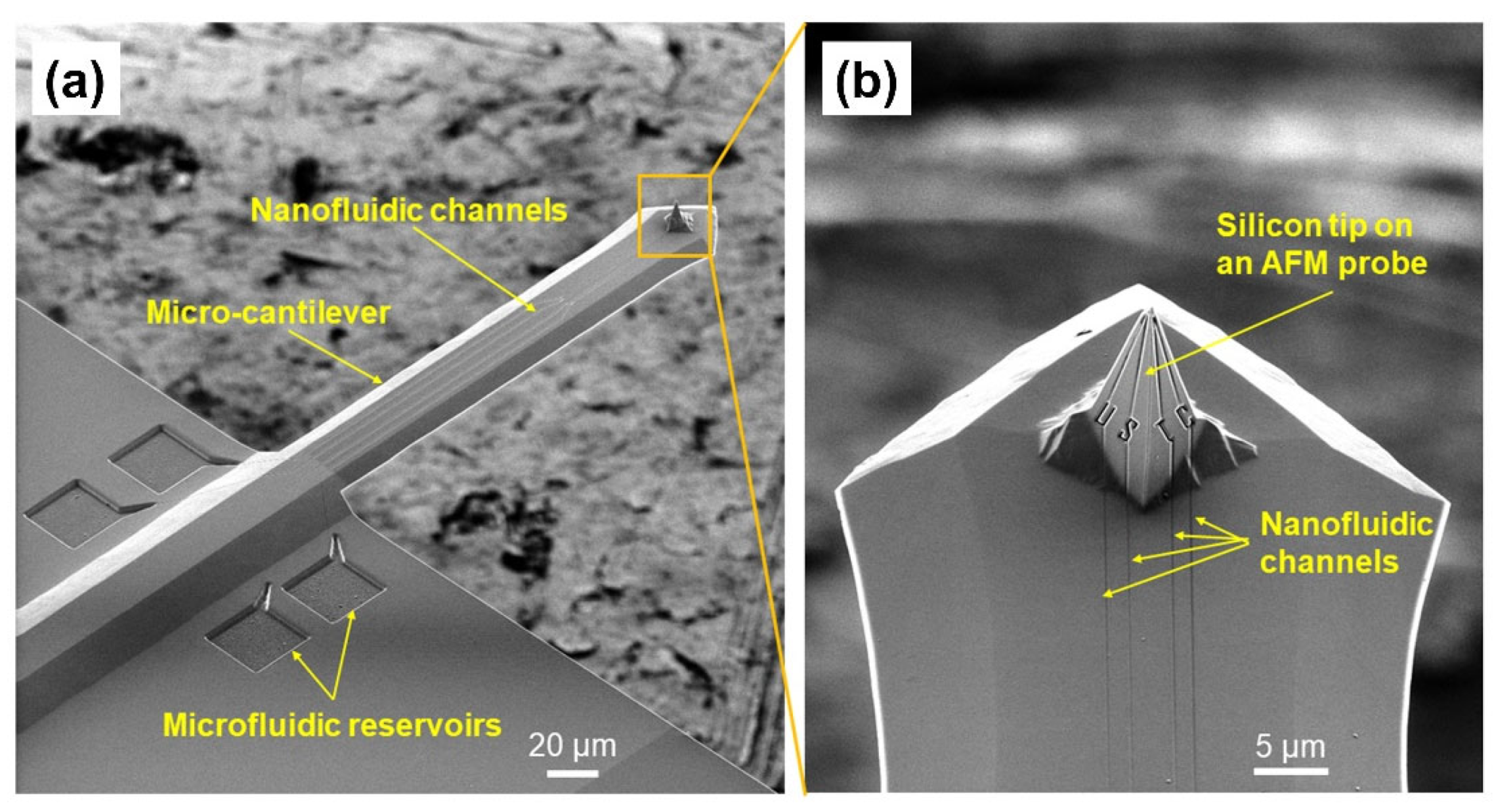
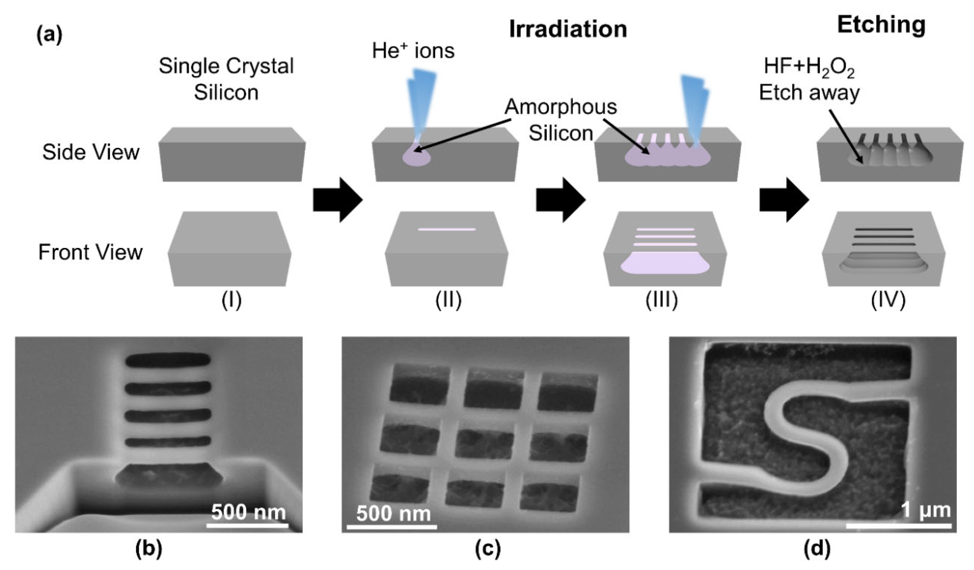
2. Results
3. Discussion
4. Conclusions
5. Experimental Section
Supplementary Materials
Author Contributions
Funding
Institutional Review Board Statement
Informed Consent Statement
Data Availability Statement
Acknowledgments
Conflicts of Interest
References
- Zhao, Y.; Saleh, A.A.E.; van de Haar, M.A.; Baum, B.; Briggs, J.A.; Lay, A.; Reyes-Becerra, O.A.; Dionne, J.A. Nanoscopic control and quantification of enantioselective optical forces. Nat. Nanotechnol. 2017, 12, 1055–1059. [Google Scholar] [CrossRef] [PubMed]
- Murphy, M.P.; Kim, S.; Sitti, M. Enhanced Adhesion by Gecko-Inspired Hierarchical Fibrillar Adhesives. ACS Appl. Mater. Interfaces 2009, 1, 849–855. [Google Scholar] [CrossRef]
- Gu, L.L.; Poddar, S.; Lin, Y.J.; Long, Z.H.; Zhang, D.Q.; Zhang, Q.P.; Shu, L.; Qiu, X.; Kam, M.; Javey, A.; et al. A biomimetic eye with a hemispherical perovskite nanowire array retina. Nature 2020, 581, 278–282. [Google Scholar] [CrossRef] [PubMed]
- Johnson, T.W.; Lapin, Z.J.; Beams, R.; Lindquist, N.C.; Rodrigo, S.G.; Novotny, L.; Oh, S.H. Highly Reproducible Near-Field Optical Imaging with Sub-20-nm Resolution Based on Template-Stripped Gold Pyramids. ACS Nano 2012, 6, 9168–9174. [Google Scholar] [CrossRef] [PubMed]
- Bleszynski-Jayich, A.C.; Shanks, W.E.; Peaudecerf, B.; Ginossar, E.; von Oppen, F.; Glazman, L.; Harris, J.G.E. Persistent Currents in Normal Metal Rings. Science 2009, 326, 272–275. [Google Scholar] [CrossRef] [PubMed]
- Linden, J.; Thanner, C.; Schaaf, B.; Wolff, S.; Lagel, B.; Oesterschulze, E. Spray coating of PMMA for pattern transfer via electron beam lithography on surfaces with high topography. Microelectron. Eng. 2011, 88, 2030–2032. [Google Scholar] [CrossRef]
- Peterson, I.R. Langmuir-Blodgett Electron-Beam Resists. IEE Proc.-I 1983, 130, 252–255. [Google Scholar] [CrossRef]
- Zhang, J.; Con, C.; Cui, B. Electron Beam Lithography on Irregular Surfaces Using an Evaporated Resist. ACS Nano 2014, 8, 3483–3489. [Google Scholar] [CrossRef]
- Yeom, J.; Shannon, M.A. Detachment Lithography of Photosensitive Polymers: A Route to Fabricating Three-Dimensional Structures. Adv. Funct. Mater. 2010, 20, 289–295. [Google Scholar] [CrossRef]
- Ward, B.W.; Notte, J.A.; Economou, N.P. Helium ion microscope: A new tool for nanoscale microscopy and metrology. J. Vac. Sci. Technol. B 2006, 24, 2871–2874. [Google Scholar] [CrossRef]
- He, S.X.; Tian, R.; Wu, W.; Li, W.D.; Wang, D.Q. Helium-ion-beam nanofabrication: Extreme processes and applications. Int. J. Extreme Manuf. 2021, 3, 012001. [Google Scholar] [CrossRef]
- Lemme, M.C.; Bell, D.C.; Williams, J.R.; Stern, L.A.; Baugher, B.W.H.; Jarillo-Herrero, P.; Marcus, C.M. Etching of Graphene Devices with a Helium Ion Beam. ACS Nano 2009, 3, 2674–2676. [Google Scholar] [CrossRef] [PubMed]
- Abbas, A.N.; Liu, G.; Liu, B.L.; Zhang, L.Y.; Liu, H.; Ohlberg, D.; Wu, W.; Zhou, C.W. Patterning, Characterization, and Chemical Sensing Applications of Graphene Nanoribbon Arrays Down to 5 nm Using Helium Ion Beam Lithography. ACS Nano 2014, 8, 1538–1546. [Google Scholar] [CrossRef] [PubMed]
- Chen, Y.Q.; Hu, Y.Q.; Zhao, J.Y.; Deng, Y.S.; Wang, Z.L.; Cheng, X.; Lei, D.Y.; Deng, Y.B.; Duan, H.G. Topology Optimization-Based Inverse Design of Plasmonic Nanodimer with Maximum Near-Field Enhancement. Adv. Funct. Mater. 2020, 30, 2000642. [Google Scholar] [CrossRef]
- Wang, Y.; Abb, M.; Boden, S.A.; Aizpurua, J.; de Groot, C.H.; Muskens, O.L. Ultrafast Nonlinear Control of Progressively Loaded, Single Plasmonic Nanoantennas Fabricated Using Helium Ion Milling. Nano Lett. 2013, 13, 5647–5653. [Google Scholar] [CrossRef]
- Scholder, O.; Jefimovs, K.; Shorubalko, I.; Hafner, C.; Sennhauser, U.; Bona, G.L. Helium focused ion beam fabricated plasmonic antennas with sub-5 nm gaps. Nanotechnology 2013, 24, 395301. [Google Scholar] [CrossRef] [PubMed]
- Yang, J.J.; Ferranti, D.C.; Stern, L.A.; Sanford, C.A.; Huang, J.; Ren, Z.; Qin, L.C.; Hall, A.R. Rapid and precise scanning helium ion microscope milling of solid-state nanopores for biomolecule detection. Nanotechnology 2011, 22, 285310. [Google Scholar] [CrossRef]
- Emmrich, D.; Beyer, A.; Nadzeyka, A.; Bauerdick, S.; Meyer, J.C.; Kotakoski, J.; Golzhauser, A. Nanopore fabrication and characterization by helium ion microscopy. Appl. Phys. Lett. 2016, 108, 163103. [Google Scholar] [CrossRef]
- Livengood, R.H.; Greenzweig, Y.; Liang, T.; Grumski, M. Helium ion microscope invasiveness and imaging study for semiconductor applications. J. Vac. Sci. Technol. B 2007, 25, 2547–2552. [Google Scholar] [CrossRef]
- Allen, F.I. A review of defect engineering, ion implantation, and nanofabrication using the helium ion microscope. Beilstein J. Nanotechnol. 2021, 12, 633–664. [Google Scholar] [CrossRef]
- Li, W.D.; Wu, W.; Williams, R.S. Combined helium ion beam and nanoimprint lithography attains 4 nm half-pitch dense patterns. J. Vac. Sci. Technol. B 2012, 30, 06F304. [Google Scholar] [CrossRef]
- Jadwiszczak, J.; Keane, D.; Maguire, P.; Cullen, C.P.; Zhou, Y.B.; Song, H.D.; Downing, C.; Fox, D.; McEvoy, N.; Zhu, R.; et al. MoS2 Memtransistors Fabricated by Localized Helium Ion Beam Irradiation. ACS Nano 2019, 13, 14262–14273. [Google Scholar] [CrossRef] [PubMed]
- Fox, D.S.; Zhou, Y.B.; Maguire, P.; O’Neill, A.; O’Coileain, C.; Gatensby, R.; Glushenkov, A.M.; Tao, T.; Duesberg, G.S.; Shvets, I.V.; et al. Nanopatterning and Electrical Tuning of MoS2 Layers with a Subnanometer Helium Ion Beam. Nano Lett. 2015, 15, 5307–5313. [Google Scholar] [CrossRef]
- Nanda, G.; Goswami, S.; Watanabe, K.; Taniguchi, T.; Alkemade, P.F.A. Defect Control and n-Doping of Encapsulated Graphene by Helium-Ion-Beam Irradiation. Nano Lett. 2015, 15, 4006–4012. [Google Scholar] [CrossRef]
- Wen, X.; Mao, R.; Hu, H. 3-D Nanofabrication of Silicon and Nanostructure Fine-Tuning via Helium Ion Implantation. Adv. Mater. Interfaces 2022, 9, 2101643. [Google Scholar] [CrossRef]
- Livengood, R.; Tan, S.; Greenzweig, Y.; Notte, J.; McVey, S. Subsurface damage from helium ions as a function of dose, beam energy, and dose rate. J. Vac. Sci. Technol. B 2009, 27, 3244–3249. [Google Scholar] [CrossRef]
- Kim, C.S.; Hobbs, R.G.; Agarwal, A.; Yang, Y.; Manfrinato, V.R.; Short, M.P.; Li, J.; Berggren, K.K. Focused-helium-ion-beam blow forming of nanostructures: Radiation damage and nanofabrication. Nanotechnology 2020, 31, 045302. [Google Scholar] [CrossRef]
- Gianola, U.F. Damage to Silicon Produced by Bombardment with Helium Ions. J. Appl. Phys. 1957, 28, 868–873. [Google Scholar] [CrossRef]
- Gibbons, J.F.; Hechtl, E.O.; Tsurushima, T. Ion-Bombardment-Enhanced Etching of Silicon. Appl. Phys. Lett. 1969, 15, 117. [Google Scholar] [CrossRef]
- Kawasegi, N.; Morita, N.; Yamada, S.; Takano, N.; Oyama, T.; Ashida, K.; Taniguchi, J.; Miyamoto, I. Three-Dimensional Nanofabrication Utilizing Selective Etching of Silicon Induced by Focused Ion Beam Irradiation. JSME Int. J. Ser. C Mech. Syst. Mach. Elem. Manuf. 2006, 49, 583–589. [Google Scholar] [CrossRef][Green Version]
- Petrov, Y.V.; Grigoryev, E.A.; Sharov, T.V.; Baraban, A.P. Effect of helium ion beam treatment on wet etching of silicon dioxide. Nucl. Instrum. Methods Phys. Res. Sect. B Beam Interact. Mater. At. 2018, 418, 94–100. [Google Scholar] [CrossRef]
- Petrov, Y.V.; Sharov, T.V.; Baraban, A.P.; Vyvenko, O.F. Effect of helium ion beam treatment on the etching rate of silicon nitride. Nucl. Instrum Meth. B 2015, 349, 90–95. [Google Scholar] [CrossRef]
- Devine, R.A.B. Macroscopic and Microscopic Effects of Radiation in Amorphous SiO2. Nucl. Instrum Meth. B 1994, 91, 378–390. [Google Scholar] [CrossRef]
- Yonehara, T.; Sakaguchi, K.; Sato, N. Epitaxial Layer Transfer by Bond and Etch Back of Porous Si. Appl. Phys. Lett. 1994, 64, 2108–2110. [Google Scholar] [CrossRef]
- Ziegler, J.F.; Ziegler, M.D.; Biersack, J.P. SRIM—The stopping and range of ions in matter (2010). Nucl. Instrum Meth. B 2010, 268, 1818–1823. [Google Scholar] [CrossRef]
- Tan, S.D.; Klein, K.; Shima, D.; Livengood, R.; Mutunga, E.; Vladar, A. Mechanism and applications of helium transmission milling in thin membranes. J. Vac. Sci. Technol. B 2014, 32, 06FA01. [Google Scholar] [CrossRef]
- Nam, S.-W.; Lee, M.-H.; Lee, S.-H.; Lee, D.-J.; Rossnagel, S.M.; Kim, K.-B. Sub-10-nm Nanochannels by Self-Sealing and Self-Limiting Atomic Layer Deposition. Nano Lett. 2010, 10, 3324–3329. [Google Scholar] [CrossRef]
- Kim, C.-J.; Kim, J.Y.; Sridharan, B. Comparative evaluation of drying techniques for surface micromachining. Sens. Actuators A Phys. 1998, 64, 17–26. [Google Scholar] [CrossRef]
- Piner, R.D.; Zhu, J.; Xu, F.; Hong, S.; Mirkin, C.A. “Dip-Pen” Nanolithography. Science 1999, 283, 661–663. [Google Scholar] [CrossRef]
- Kim, K.-H.; Moldovan, N.; Espinosa, H.D. A Nanofountain Probe with Sub-100 nm Molecular Writing Resolution. Small 2005, 1, 632–635. [Google Scholar] [CrossRef]
- Lee, J.; Shen, W.; Payer, K.; Burg, T.P.; Manalis, S.R. Toward Attogram Mass Measurements in Solution with Suspended Nanochannel Resonators. Nano Lett. 2010, 10, 2537–2542. [Google Scholar] [CrossRef]
- Cermak, N.; Olcum, S.; Delgado, F.F.; Wasserman, S.C.; Payer, K.R.; Murakami, M.A.; Knudsen, S.M.; Kimmerling, R.J.; Stevens, M.M.; Kikuchi, Y.; et al. High-throughput measurement of single-cell growth rates using serial microfluidic mass sensor arrays. Nat. Biotechnol. 2016, 34, 1052–1059. [Google Scholar] [CrossRef]
- Craighead, H.G. Nanoelectromechanical systems. Science 2000, 290, 1532–1535. [Google Scholar] [CrossRef]
- Yang, Y.T.; Ekinci, K.L.; Huang, X.M.H.; Schiavone, L.M.; Roukes, M.L.; Zorman, C.A.; Mehregany, M. Monocrystalline silicon carbide nanoelectromechanical systems. Appl. Phys. Lett. 2001, 78, 162–164. [Google Scholar] [CrossRef]
- Michaels, J.A.; Janavicius, L.; Wu, X.H.; Chan, C.; Huang, H.C.; Namiki, S.; Kim, M.; Sievers, D.; Li, X.L. Producing Silicon Carbide Micro and Nanostructures by Plasma-Free Metal-Assisted Chemical Etching. Adv. Funct. Mater. 2021, 31, 2103298. [Google Scholar] [CrossRef]
- Liu, Y.-H.; Sun, Y.-J.; Zhao, G.-J.; Liao, L.-M.; Wang, T.; Chen, Z.-Z. Crystal structure induced residue formation on 4H-SiC by reactive ion etching. AIP Adv. 2016, 6, 065219. [Google Scholar] [CrossRef]
- Beheim, G.M.; Evans, L.J. Control of trenching and surface roughness in deep reactive ion etched 4H and 6H SiC. Mater. Res. Soc. Symp. Proc. 2005, 911, 1015. [Google Scholar] [CrossRef]
- Jayawardena, A.; Ahyi, A.C.; Liu, G.; Shaw, R.G.; Dhar, S. Isotropic Oxidation by Plasma Oxidation and Investigation of RIE Induced Effects for Development of 4H-SiC Trench MOSFETs. Mater. Sci. Forum 2018, 924, 444–448. [Google Scholar] [CrossRef]
- Fischer, A.C.; Belova, L.M.; Rikers, Y.G.M.; Malm, B.G.; Radamson, H.H.; Kolahdouz, M.; Gylfason, K.B.; Stemme, G.; Niklaus, F. 3D Free-Form Patterning of Silicon by Ion Implantation, Silicon Deposition, and Selective Silicon Etching. Adv. Funct. Mater. 2012, 22, 4004–4008. [Google Scholar] [CrossRef]
- Liu, Y.; Chow, C.W.; Cheung, W.Y.; Tsang, H.K. In-line channel power monitor based on helium ion implantation in silicon-on-insulator waveguides. IEEE Photonics Technol. Lett. 2006, 18, 1882–1884. [Google Scholar] [CrossRef]


Publisher’s Note: MDPI stays neutral with regard to jurisdictional claims in published maps and institutional affiliations. |
© 2022 by the authors. Licensee MDPI, Basel, Switzerland. This article is an open access article distributed under the terms and conditions of the Creative Commons Attribution (CC BY) license (https://creativecommons.org/licenses/by/4.0/).
Share and Cite
Wen, X.; Zhang, L.; Tian, F.; Xu, Y.; Hu, H. Versatile Approach of Silicon Nanofabrication without Resists: Helium Ion-Bombardment Enhanced Etching. Nanomaterials 2022, 12, 3269. https://doi.org/10.3390/nano12193269
Wen X, Zhang L, Tian F, Xu Y, Hu H. Versatile Approach of Silicon Nanofabrication without Resists: Helium Ion-Bombardment Enhanced Etching. Nanomaterials. 2022; 12(19):3269. https://doi.org/10.3390/nano12193269
Chicago/Turabian StyleWen, Xiaolei, Lansheng Zhang, Feng Tian, Yang Xu, and Huan Hu. 2022. "Versatile Approach of Silicon Nanofabrication without Resists: Helium Ion-Bombardment Enhanced Etching" Nanomaterials 12, no. 19: 3269. https://doi.org/10.3390/nano12193269
APA StyleWen, X., Zhang, L., Tian, F., Xu, Y., & Hu, H. (2022). Versatile Approach of Silicon Nanofabrication without Resists: Helium Ion-Bombardment Enhanced Etching. Nanomaterials, 12(19), 3269. https://doi.org/10.3390/nano12193269