
Solution Processed Zn1−x−ySmxCuyO Nanorod Arrays for Dye Sensitized Solar Cells

 , ,
, ,  ,
,  , and
, and
Abstract
1. Introduction
2. Experimental Details
2.1. Chemicals
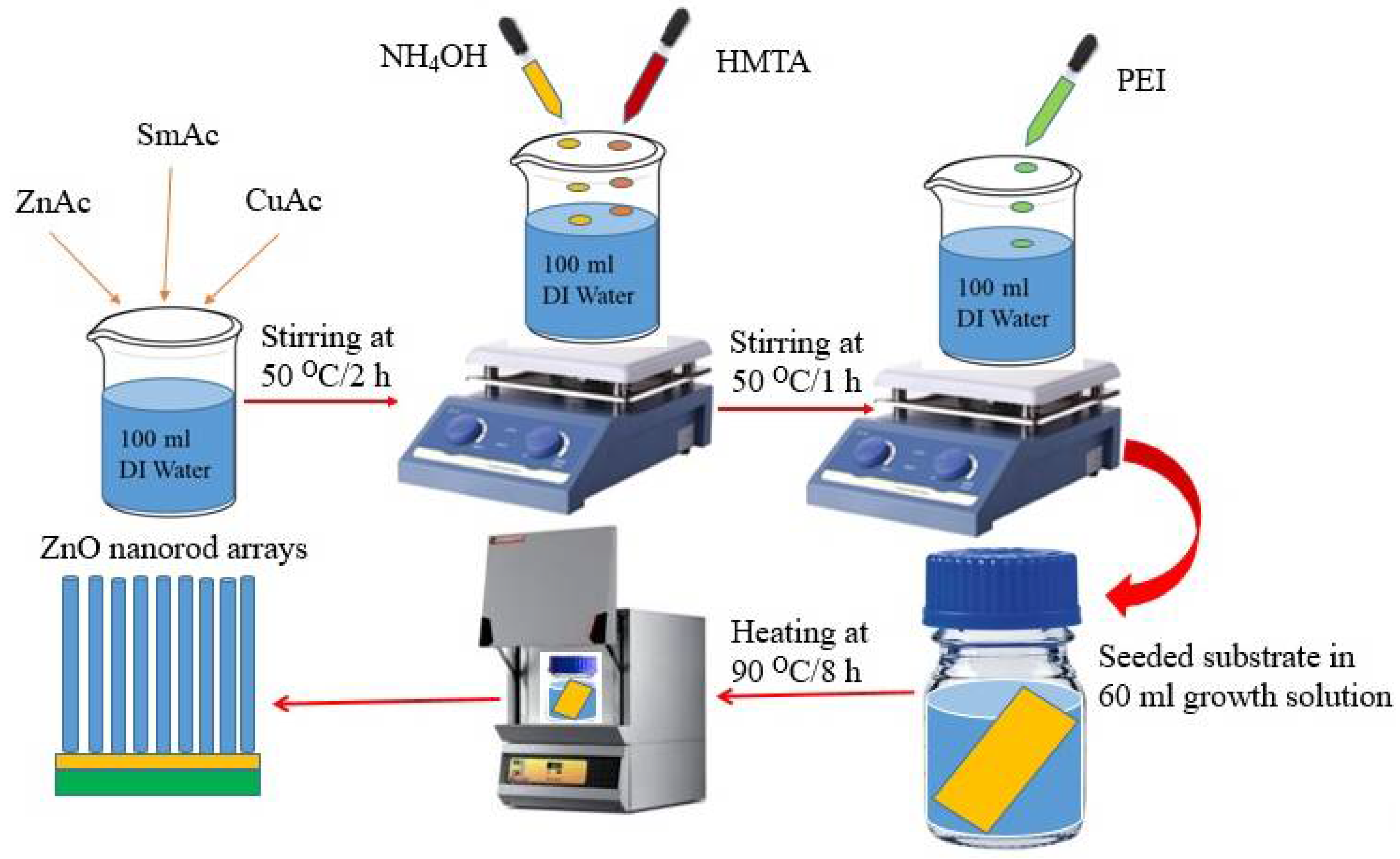
2.2. Methods
2.2.1. Spin Coating of Seed Layer
2.2.2. Nanorod Arrays Growth
2.3. Dye-Sensitized Solar Cell Fabrication
2.4. Characterization and Measurements
3. Results and Discussion
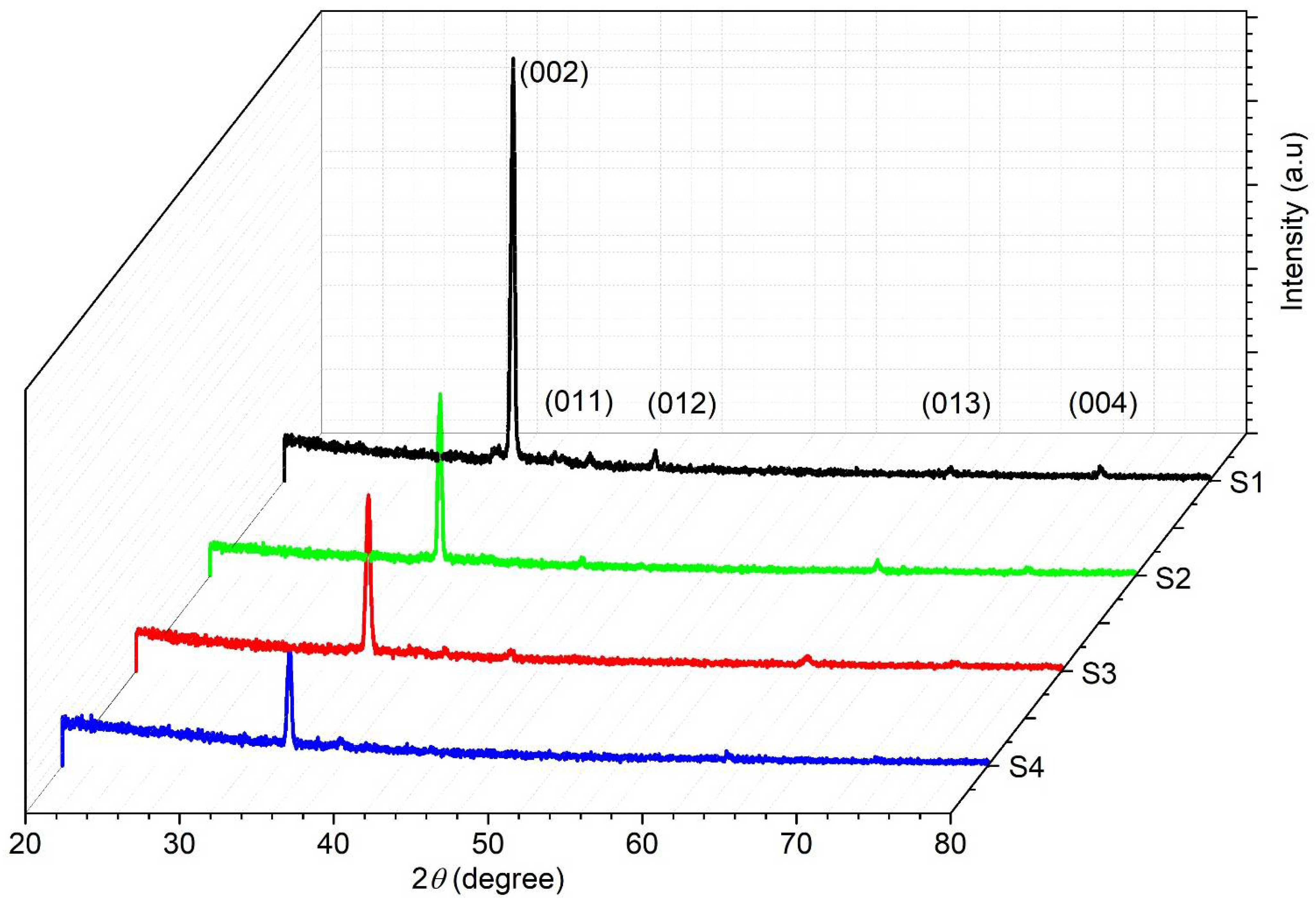
3.1. Crystal Structure of Nanorod Arrays
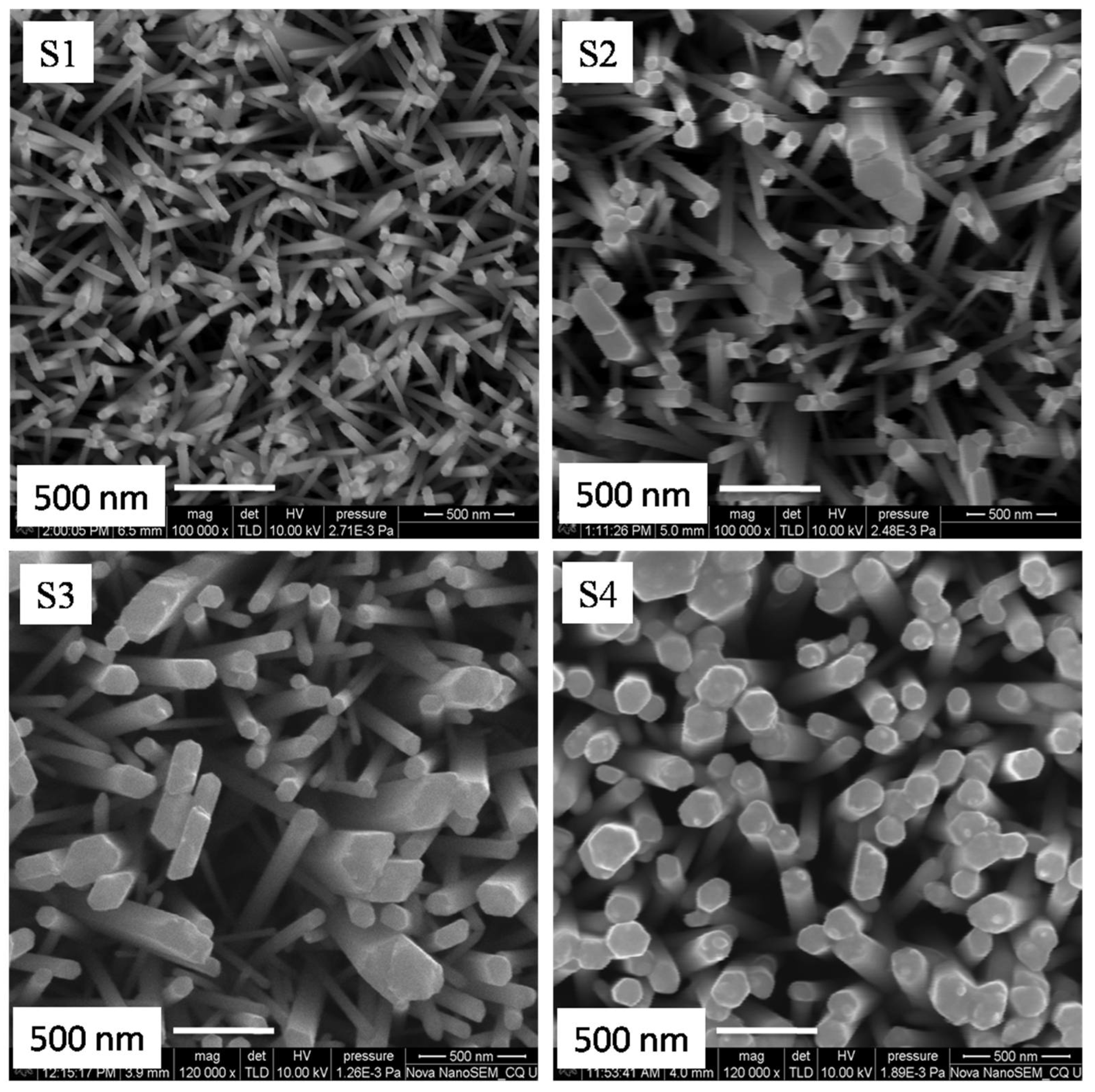
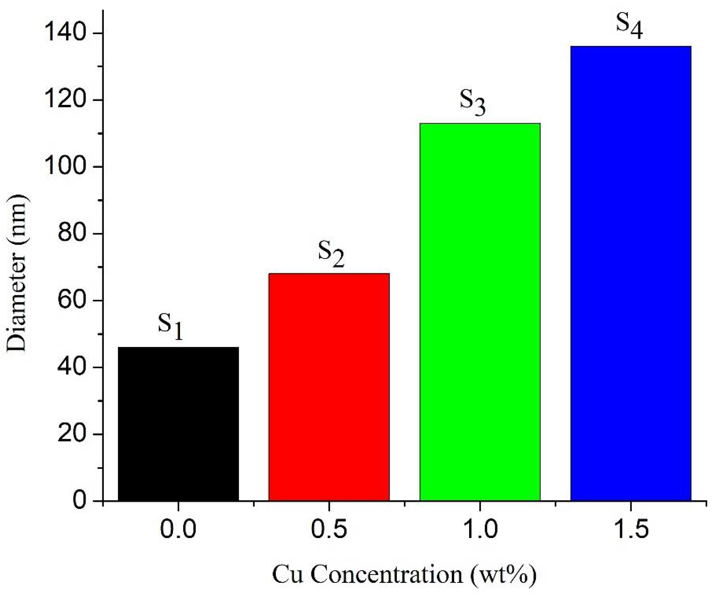
3.2. Surface Morphology of Nanorod Arrays
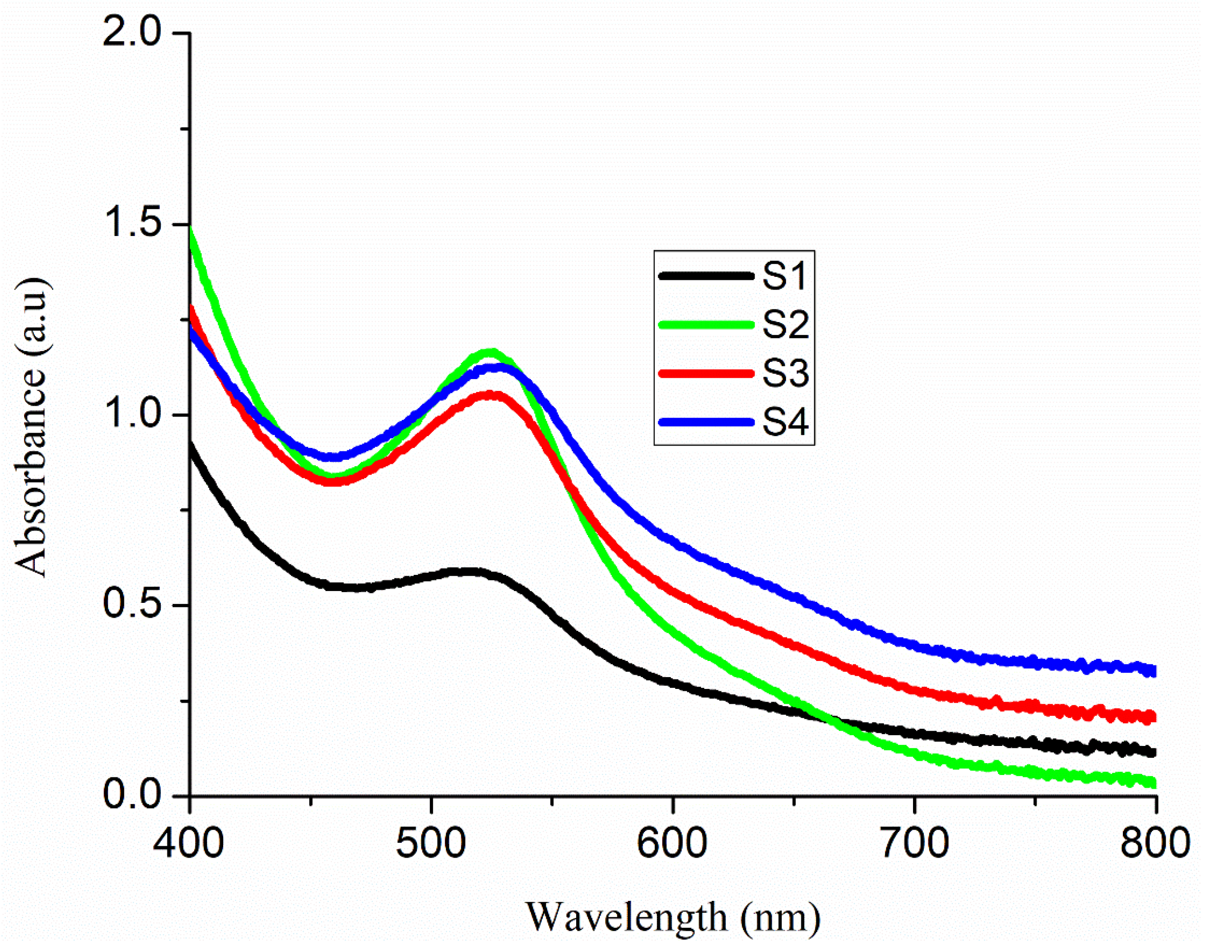
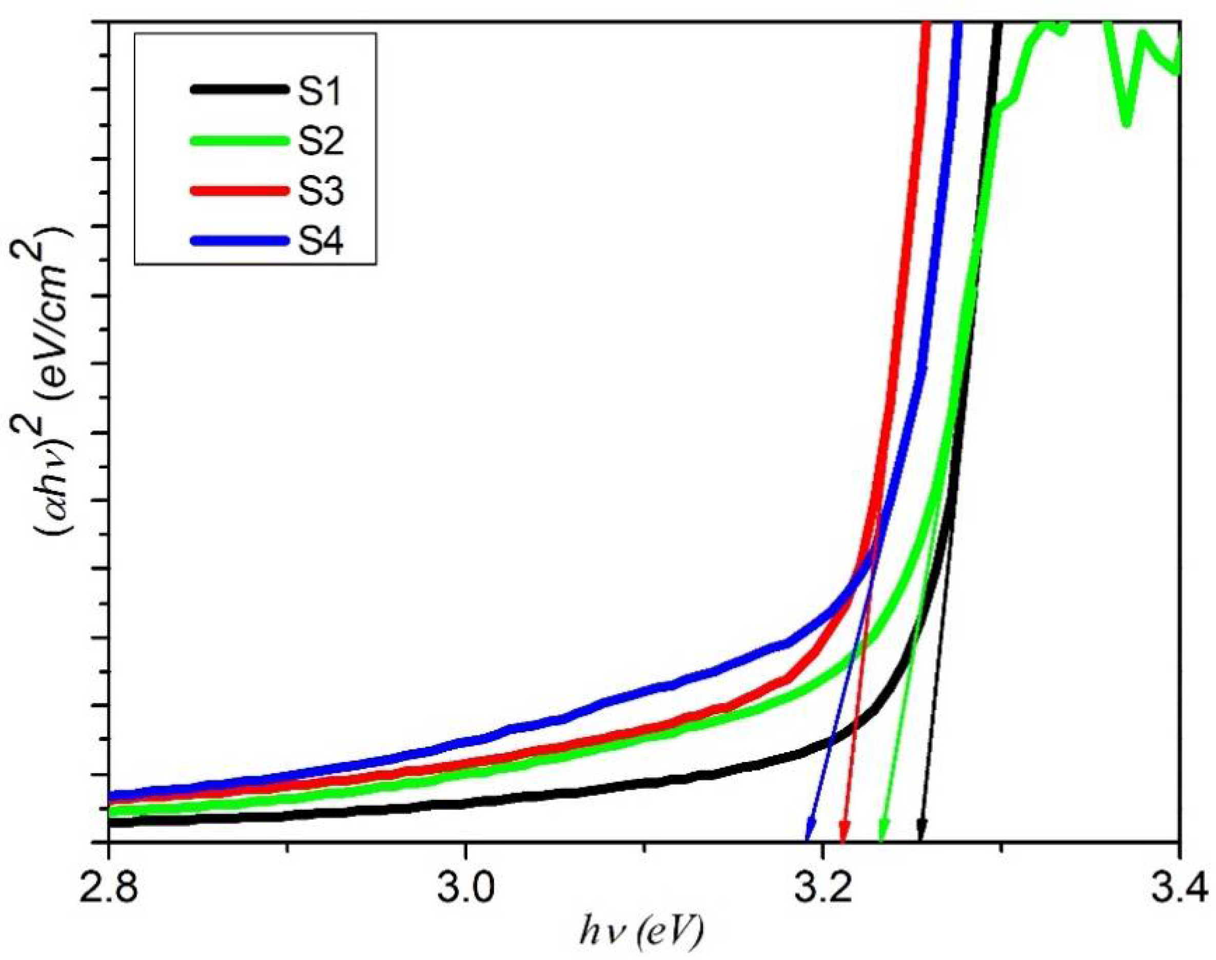
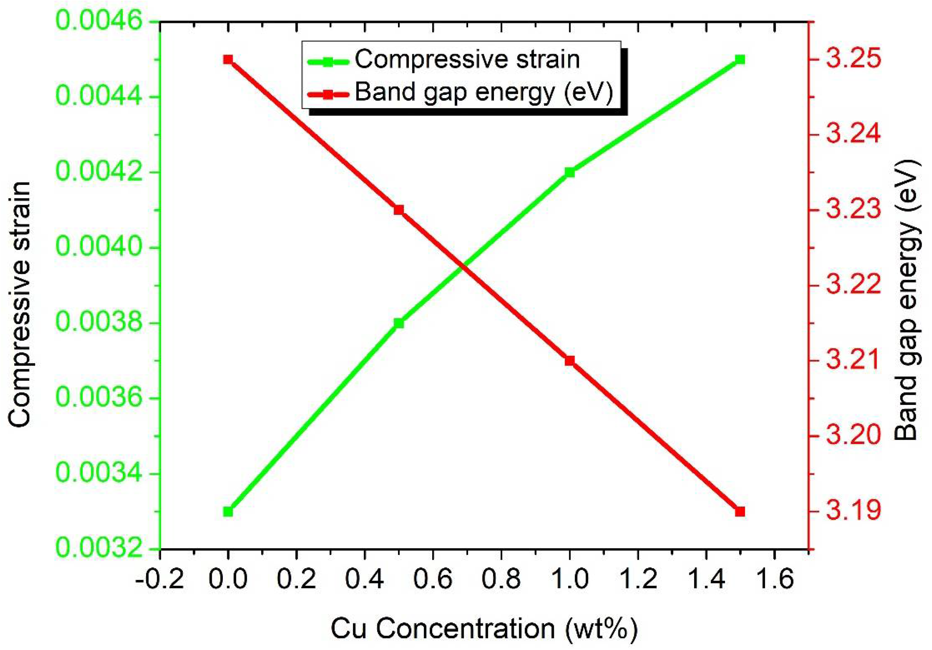
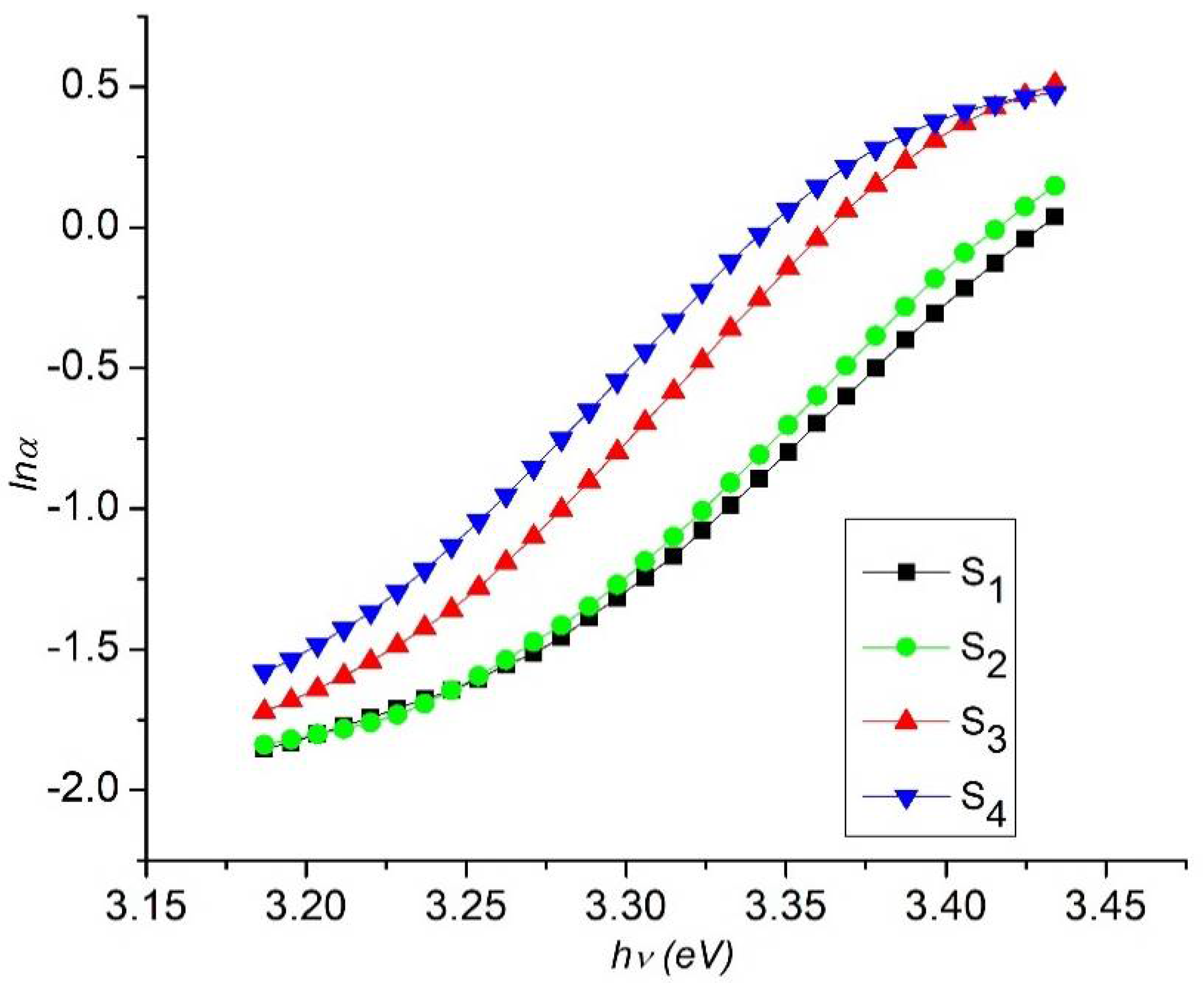
3.3. Optical Measurement of Nanorod Arrays
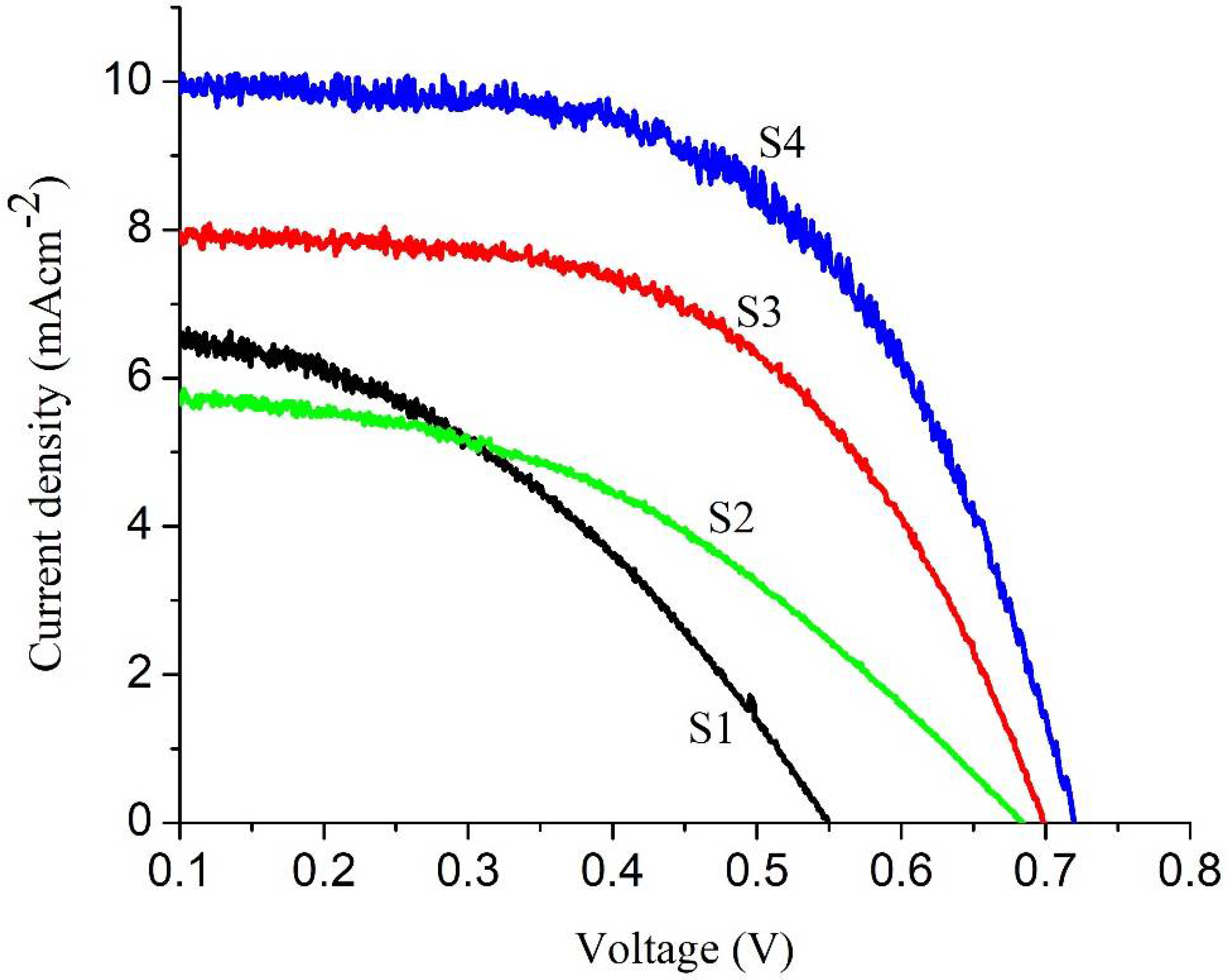
3.4. I-V Measurements of Cu-Doped ZnO-Sm Films
4. Conclusions
Author Contributions
Funding
Data Availability Statement
Acknowledgments
Conflicts of Interest
References
- Zhang, L.; Wang, Y.; Wu, H.; Hou, M.; Wang, J.; Zhang, L.; Liao, C.; Liu, S. A ZnO nanowire-based microfiber coupler for all-optical photodetection applications. Nanoscale 2019, 11, 8319–8326. [Google Scholar] [CrossRef]
- Yu, C.; Pana, Z.L.; Wang, R. High performance of ZnO nanowireprotein sensors enhanced by the piezotronic effect. Energy Environ. Sci. 2013, 6, 494. [Google Scholar] [CrossRef]
- Fu, S.; Zhang, B.; Hu, H.; Zhang, Y.; Bi, Y. ZnO nanowire arrays decorated with PtO nanowires for efficient solar water splitting. Catal. Sci. Technol. 2018, 8, 2789–2793. [Google Scholar] [CrossRef]
- Wang, X.; Song, J.; Wang, Z.L. Nanowire and nanobelt arrays of zinc oxide from synthesis to properties and to novel devices. J. Mater. Chem. 2007, 17, 711–720. [Google Scholar] [CrossRef]
- Chang, J.; Lin, W.; Hon, M. Effects of post-annealing on the structure and properties of Al-doped zinc oxide films. Appl. Surf. Sci. 2001, 183, 18–25. [Google Scholar] [CrossRef]
- Rackauskas, S.; Barbero, N.; Barolo, C.; Viscardi, G. ZnO Nanowires for Dye Sensitized Solar Cells. Nanowires New Insights 2017, 60–78. [Google Scholar] [CrossRef]
- Giannouli, M.; Govatsi, K.; Syrrokostas, G.; Yannopoulos, S.N.; Leftheriotis, G. Factors Affecting the Power Conversion Effi-ciency in ZnO DSSCs: Nanowire vs. Nanoparticles. Materials 2018, 1, 11. [Google Scholar]
- Yu, K.; Chen, J. Enhancing Solar Cell Efficiencies through 1-D Nanostructures. Nanoscale Res. Lett. 2008, 4, 1–10. [Google Scholar] [CrossRef]
- Sharma, K.; Sharma, V.; Sharma, S.S. Dye-Sensitized Solar Cells: Fundamentals and Current Status. Nanoscale Res. Lett. 2018, 13, 381. [Google Scholar] [CrossRef]
- Galliano, S.; Federico, B.; Bonomo, M.; Viscardi, G.; Gerbaldi, C.; Boschloo, C.; Barolo, C. Hydrogel Electrolytes Based on Xanthan Gum: Green Route towards Stable Dye-Sensitized Solar Cells. Nanomaterials 2020, 10, 1585. [Google Scholar] [CrossRef]
- Nicole, M.; Matteo, B.; Lucia, F.; Nadia, B.; Claudio, G.; Federico, B.; Claudia, B. Recent advances in eco-friendly and cost-effective materials towards sustainable dye-sensitized solar cells. Green Chem. 2020, 21, 7168–7218. [Google Scholar]
- Antonio, C.; Roberto, C.; Fabio, B.; Maria, T.; Trifuoggi, M.; Federico, B.; Claudio, G.; Simone, G.; Eduardo, S.; Arianna, M.; et al. Tuning optical and electronic properties in novel carbazole photosensitizers for p-type dye-sensitized solar cells. Electrochim. Acta 2018, 292, 805–816. [Google Scholar]
- Pulli, E.; Rozzi, E.; Bella, F. Transparent photovoltaic technologies: Current trends towards upscaling. Energy Convers. Manag. 2020, 219, 112982. [Google Scholar] [CrossRef]
- Brishty, D.C.; Chen, L.; Sk, M.A.Z.S.; Javier, S.-M.; Hasina, H.; Mohammed, J.U. A photoanode with hierarchical nanoforest TiO2 structure and silver plasmonic nanoparticles for fexible dye sensitized solar cell. Sci. Rep. 2021, 11, 7552. [Google Scholar]
- Fagiolari, L.; Bonomo, M.; Cognetti, A.; Meligrana, G.; Gerbaldi, C.; Barolo, C.; Bella, F. Photoanodes for Aqueous Solar Cells: Exploring Additives and Formulations Starting from a Commercial TiO2 Paste. ChemSusChem 2020, 13, 6562–6573. [Google Scholar] [CrossRef] [PubMed]
- Galliano, S.; Federico, B.; Matteo, B.; Fabrizio, G.; Michael, G.; Guido, V.; Anders, H.; Claudio, G.; Claudia, B. Xanthan-Based Hydrogel for Stable and Efficient Quasi-Solid Truly Aqueous Dye-Sensitized Solar Cell with Cobalt Mediator. Solar Rrl 2021, 2000823. [Google Scholar] [CrossRef]
- Patil, S.S.; Mane, R.M.; Khot, K.V.; Mali, S.S.; Hong, C.K.; Bhosale, P.N. Surfactant assisted approach to development of efficient WO3 photoanode for natural dye sensitized solar cell. Sol. Energy 2021, 220, 371–383. [Google Scholar] [CrossRef]
- Federico, B.; Claudio, G.; Claudia, B.; Michael, G. Aqueous dye-sensitized solar cells. Chem. Soc. Rev. 2015, 44, 3431–3473. [Google Scholar]
- Wu, G.R.; Chen, H.H.; Yang, C.H.; Ku, J.Y.; Lai, J.J. Effects of dye adsorption on the electron transport properties in ZnO-nanowire dye-sensitized solar cells. Appl. Phys. Lett. 2007, 90, 213109. [Google Scholar] [CrossRef]
- Ma, L.; Ma, S.; Chen, H.; Ai, X.; Huang, X. Microstructures and optical properties of Cu-doped ZnO films prepared by radio frequency reactive magnetron sputtering. Appl. Surf. Sci. 2011, 257, 10036–10041. [Google Scholar] [CrossRef]
- Jeon, J.H.; Jeong, S.Y.; Cho, C.R.; Lee, S.-A.; Ahn, H.-S.; Kim, H.-S. Heteroepitaxial relation and optical properties of Cu-doped ZnO flms grown by using pulsed laser deposition. J. Kor. Phys. Soc. 2009, 54, 858–862. [Google Scholar] [CrossRef]
- Bedir, M.; Oztas, M.; Yazici, A.N.; Kafadar, E.V. Characterization of undoped and Cu-Doped ZnO Tin flms deposited on glass substrates by spray pyrolysis. Chin. Phys. Lett. 2006, 23, 939–942. [Google Scholar] [CrossRef]
- Chandrasekar, L.B.; Chandramohan, R.; Vijayalakshmi, R.; Chandrasekaran, S. Preparation and characterization of Mn-doped ZnS nanoparticles. Int. Nano Lett. 2015, 5, 71–75. [Google Scholar] [CrossRef]
- Chandrasekar, L.; Bruno, R.; Chandramohan, S.; Thirumalai, J.; Vijayalakshmi, R. Luminescence and Unit Cell Analysis of Zn1−xCdxO Nanoparticles. Adv. Sci. Focus 2013, 1, 292–296. [Google Scholar] [CrossRef]
- Vinod Kumar, O.M.; Ntwaeaborwa, T.; Soga, V.D.; Swart, H.C. Rare Earth Doped Zinc Oxide Nanophosphor Powder: A Future Material for Solid State Lighting and Solar Cells. ACS Photon. 2017, 4, 2613–2637. [Google Scholar] [CrossRef]
- Daksh, D.; Agrawal, Y.K. Rare Earth-Doped Zinc Oxide Nanostructures: A Review. Rev. Nanosci. Nanotechnol. 2016, 5, 1–27. [Google Scholar] [CrossRef]
- Sin, J.C.; Lam, S.M.; Lee, K.T.; Mohamed, A.R. Preparation and photocatalytic properties of visible light-driven samarium-doped ZnO nanorods. Ceram. Int. 2013, 39, 5833–5843. [Google Scholar] [CrossRef]
- Wang, X.; Kong, X.; Shan, G.; Yu, Y.; Sun, Y.; Feng, L.; Li, Y. Luminescence spectroscopy and visible upconversion properties of Er3+ in ZnO nanocrystals. J. Phys. Chem. B 2004, 108, 18408–18413. [Google Scholar] [CrossRef]
- Wei, S.; Chen, Y.; Ma, Y.; Shao, Z. Fabrication of CuO/ZnO composite films with cathodic co-electrode position and their photocatalytic performance. J. Molec. Catal. A Chem. 2010, 331, 112–116. [Google Scholar] [CrossRef]
- Zhang, L.; Wu, C.; Liu, W.; Yang, S.; Wang, M.; Chen, T.; Zhu, C. Sequential deposition route to efficient Sb2S3 solar cells. J. Mater. Chem. A 2018, 6, 21320–21326. [Google Scholar] [CrossRef]
- Zhang, X.F.; Liu, Z.G.; Shen, W.; Gurunathan, S. Silver nanoparticles: Synthesis, characterization, properties, applications, and therapeutic approaches. Int. J. Molec. Sci. 2016, 17, 1534. [Google Scholar] [CrossRef] [PubMed]
- Yao, J.; Huang, K.; Fu, X.; Deng, M.; Ding, X.; Xu, Z.; Zhang, S. Improving photovoltaic performance of dye sensitized solar cells based on a hierarchical structure with up/down converter. RSC Adv. 2016, 6, 11880–11887. [Google Scholar] [CrossRef]
- Yao, N.; Huang, J.; Fu, K.; Deng, X.; Ding, M.; Shao, M.; Xu, X. Enhanced light harvesting of dye-sensitized solar cells with up/down conversion materials. Electrochim. Acta 2015, 154, 273–277. [Google Scholar] [CrossRef]
- Tyona, M.D.; Osuji, R.; Asogwa, P.; Jambure, S.; Ezema, F. Structural modification and band gap tailoring of zinc oxide thin films using copper impurities. J. Solid State Electrochem. 2017, 21, 2629–2638. [Google Scholar] [CrossRef]
- Singhal, S.; Kaur, J.; Namgyal, T.; Sharma, R. Cu-doped ZnO nanoparticles: Synthesis, structural and electrical properties. Phys. B Condens. Matter 2012, 407, 1223–1226. [Google Scholar] [CrossRef]
- Muhammad, S.; Kashif, I.; Saif, U.R.; Sufyan Javed, M.; Mohd, A.H.; Hafiz, M.A.; Amjad, A.; Muhammad, Z.M.; Saiful, I. Characteristics and Photovoltaic Applications of Au-Doped ZnO–Sm Na-noparticle Films. Nanomaterials 2021, 11, 702. [Google Scholar]
- Saleem, M.; Fang, L.; Huang, Q.L.; Li, D.C.; Wu, F.; Ruan, H.B.; Kong, C.Y. Annealing treatment of zno thin films deposited by sol–gel method. Surf. Rev. Lett. 2012, 19, 1250055. [Google Scholar] [CrossRef]
- Babikier, M.; Wang, D.; Wang, J.; Li, Q.; Sun, J.; Yan, Y.; Yu, Q.; Jiao, S. Cu-doped ZnO nanorod arrays: The effects of copper precursor and concentration. Nanoscale Res. Lett. 2014, 9, 199. [Google Scholar] [CrossRef][Green Version]
- Okur, H.E.; Bulut, N.; Ates, T.; Kayğili, Ö. Structural and optical characterization of Sm-doped ZnO nanoparticles. Bull. Mater. Sci. 2019, 42, 199. [Google Scholar] [CrossRef]
- Chow, L.; Lupan, O.; Chai, G.; Khallaf, H.; Ono, L.; Cuenya, B.R.; Tiginyanu, I.; Ursaki, V.; Sontea, V.; Schulte, A. Synthesis and characterization of Cu-doped ZnO one-dimensional structures for miniaturized sensor applications with faster response. Sens. Actuators A Phys. 2013, 189, 399–408. [Google Scholar] [CrossRef]
- Dom, R.; Lijin, R.B.; Kim, H.G.; Borse, P.H. Enhanced solar photoelectrochemical conversion efficiency of ZnO:cu electrodes for water-splitting application. Int. J. Photoener. 2013, 2013, 928321. [Google Scholar] [CrossRef]
- Fons, P.; Yamada, A.; Iwata, K.; Matsubara, K.; Niki, S.; Nakahara, K.; Takasu, H. An EXAFS and XANES study of MBE grown Cu-doped ZnO. Nucl. Instruments Meth. Phys. Res. Sect. B: Beam Interact. Mater. Atoms 2003, 199, 190–194. [Google Scholar] [CrossRef]
- Fons, P.; Nakahara, K.; Yamada, A.; Iwata, K.; Matsubara, H.; Takusu, S.; Niki, S. A XANES study of Cu valency in Cu-doped epitaxial ZnO. Phys. Stat. Sol. B 2002, 229, 849–852. [Google Scholar] [CrossRef]
- Wahl, U.; Rita, E.; Correia, J.G.; Agne, T.; Alves, E.; Soares, J.C. The ISOLDE Collaboration. Lattice sites of implanted Cu and Ag in ZnO. Superlatt. Micro Struct. 2006, 39, 229–237. [Google Scholar] [CrossRef][Green Version]
- Kanade, K.; Kale, B.; Baeg, J.-O.; Lee, S.M.; Lee, C.W.; Moon, S.-J.; Chang, H. Self-assembled aligned Cu doped ZnO nanoparticles for photocatalytic hydrogen production under visible light irradiation. Mater. Chem. Phys. 2007, 102, 98–104. [Google Scholar] [CrossRef]
- Rajesh, K.; Ahmad, U.; Girish, K.; Hari, S.N.; Anil Kumar, M.; Akhtar, S. Zinc oxide nanostructure-based dye-sensitized solar cells (Review). J. Mater. Sci. 2017, 52, 4743–4795. [Google Scholar]
- Zhang, L.; Yulin, Y.; Ruiqing, F.; Jia, Y.; Liang, L. Improving the efficiency of ZnO-based dye-sensitized solar cells by Pr and N co-doping. J. Mater. Chem. A 2013, 39, 12066–12073. [Google Scholar] [CrossRef]
- Zhao, J.-X.; Lu, X.-H.; Zheng, Y.-Z.; Bi, S.-Q.; Tao, X.; Chen, J.-F.; Zhou, W. Eu doping for hierarchical ZnO nanocrystalline aggregates based dye-sensitized solar cell. Electrochem. Commun. 2013, 32, 14–17. [Google Scholar] [CrossRef]
- Lu, L.; Renjie, L.; Tianyou, P.; Ke, F.; Ke, D. Effects of rare earth ion modifications on the photoelectrochemical properties of ZnO-based dye-sensitized solar cells. Renew. Energ. 2011, 36, 3386–3393. [Google Scholar] [CrossRef]
- Roose, B.; Sandeep, P.; Ullrich, S. Doping of TiO2 for sensitized solar cells. Chem. Soc. Rev. 2015, 44, 8326–8349. [Google Scholar] [CrossRef] [PubMed]
- Cheben, P.; Halir, R.; Schmid, J.H.; Atwater, H.A.; Smith, D.R. Subwavelength integrated photonics. Nat. Cell Biol. 2018, 560, 565–572. [Google Scholar] [CrossRef] [PubMed]
- Li, K.; Haque, S.; Martins, A.; Fortunato, E.; Martins, R.; Mendes, M.J.; Schuster, C.S. Light Trapping in Solar Cells: Simple Design Rules to Maximize Absorption. Optica 2020, 7, 1377–1384. [Google Scholar] [CrossRef]


| Samples | Zn1−x−ySmxCuyO | Content of Sm (wt%) | Content of Cu (wt%) |
|---|---|---|---|
| S1 | Zn1−x−ySmxCuyO | 1 | 0.0 |
| S2 | Zn1−x−ySmxCuyO | 1 | 0.5 |
| S3 | Zn1−x−ySmxCuyO | 1 | 1.0 |
| S4 | Zn1−x−ySmxCuyO | 1 | 1.5 |
| Samples | FWHM (β) | Crystallite Size (D) (nm) | Compressive Strain | d-Spacing (d) (nm) | Dislocation Density (nm)−2 | Band Gap (Eg) (eV) |
|---|---|---|---|---|---|---|
| S1 | 0.2385 | 36.48 | 0.0033 | 0.256 | 0.0007 | 3.25 |
| S2 | 0.2714 | 32.07 | 0.0038 | 0.257 | 0.0010 | 3.23 |
| S3 | 0.3001 | 28.99 | 0.0042 | 0.258 | 0.0012 | 3.21 |
| S4 | 0.3261 | 26.68 | 0.0045 | 0.260 | 0.0014 | 3.19 |
| Cell Parameters | Samples | |||
|---|---|---|---|---|
| S1 | S2 | S3 | S4 | |
| Jsc (mA/cm2) | 6.32 ± 0.046 | 5.84 ± 0.017 | 7.87 ± 0.021 | 9.99 ± 0.011 |
| Voc (V) | 0.550 ± 0.002 | 0.681 ± 0.005 | 0.692 ± 0.004 | 0.725 ± 0.003 |
| FF | 0.43 ± 0.003 | 0.51 ± 0.006 | 0.67 ± 0.003 | 0.63 ± 0.004 |
| η (%) | 1.74 ± 0.001 | 2.47 ± 0.012 | 3.30 ± 0.002 | 4.14 ± 0.001 |
Publisher’s Note: MDPI stays neutral with regard to jurisdictional claims in published maps and institutional affiliations. |
© 2021 by the authors. Licensee MDPI, Basel, Switzerland. This article is an open access article distributed under the terms and conditions of the Creative Commons Attribution (CC BY) license (https://creativecommons.org/licenses/by/4.0/).
Share and Cite
Saleem, M.; Algahtani, A.; Rehman, S.U.; Javed, M.S.; Irshad, K.; Ali, H.M.; Malik, M.Z.; Ali, A.; Tirth, V.; Islam, S. Solution Processed Zn1−x−ySmxCuyO Nanorod Arrays for Dye Sensitized Solar Cells. Nanomaterials 2021, 11, 1710. https://doi.org/10.3390/nano11071710
Saleem M, Algahtani A, Rehman SU, Javed MS, Irshad K, Ali HM, Malik MZ, Ali A, Tirth V, Islam S. Solution Processed Zn1−x−ySmxCuyO Nanorod Arrays for Dye Sensitized Solar Cells. Nanomaterials. 2021; 11(7):1710. https://doi.org/10.3390/nano11071710
Chicago/Turabian StyleSaleem, Muhammad, Ali Algahtani, Saif Ur Rehman, Muhammad Sufyan Javed, Kashif Irshad, Hafiz Muhammad Ali, Muhammad Zeeshan Malik, Amjad Ali, Vineet Tirth, and Saiful Islam. 2021. "Solution Processed Zn1−x−ySmxCuyO Nanorod Arrays for Dye Sensitized Solar Cells" Nanomaterials 11, no. 7: 1710. https://doi.org/10.3390/nano11071710
APA StyleSaleem, M., Algahtani, A., Rehman, S. U., Javed, M. S., Irshad, K., Ali, H. M., Malik, M. Z., Ali, A., Tirth, V., & Islam, S. (2021). Solution Processed Zn1−x−ySmxCuyO Nanorod Arrays for Dye Sensitized Solar Cells. Nanomaterials, 11(7), 1710. https://doi.org/10.3390/nano11071710