
Investigate on the Mechanism of HfO2/Si0.7Ge0.3 Interface Passivation Based on Low-Temperature Ozone Oxidation and Si-Cap Methods

 , , and
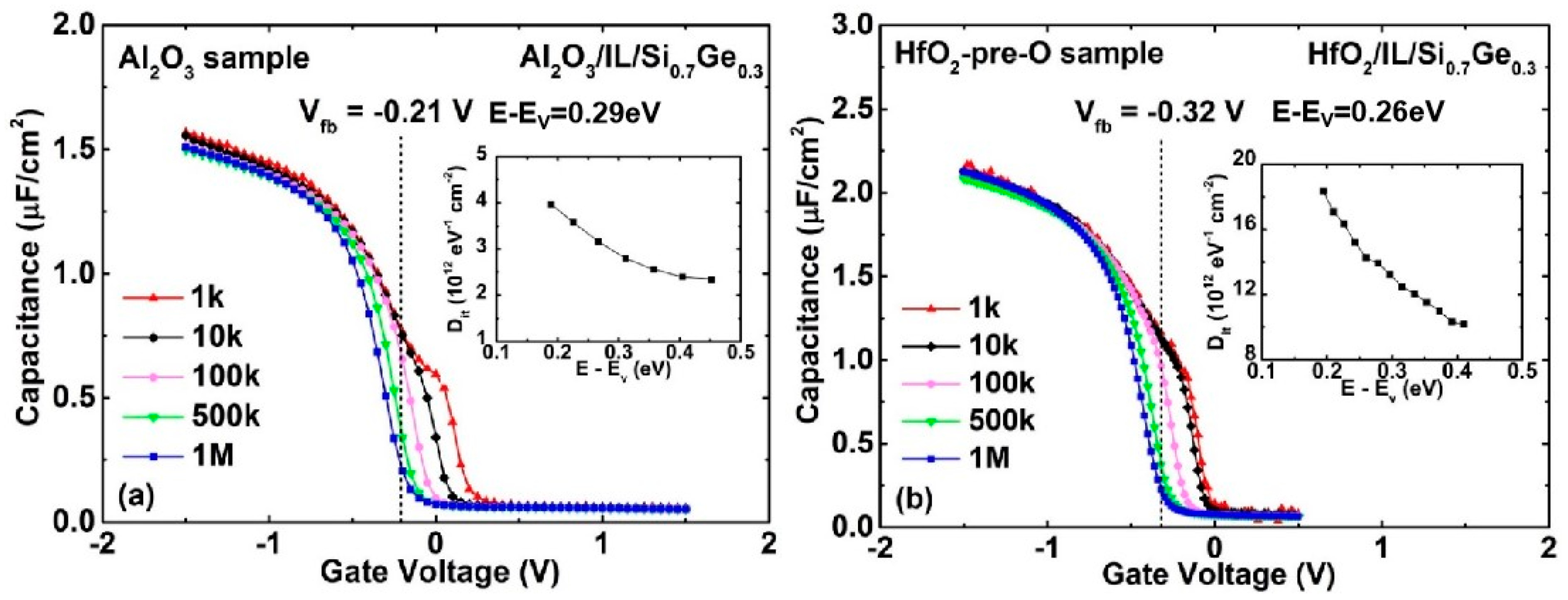
Abstract
1. Introduction
2. Materials and Methods
3. Results and Discussion
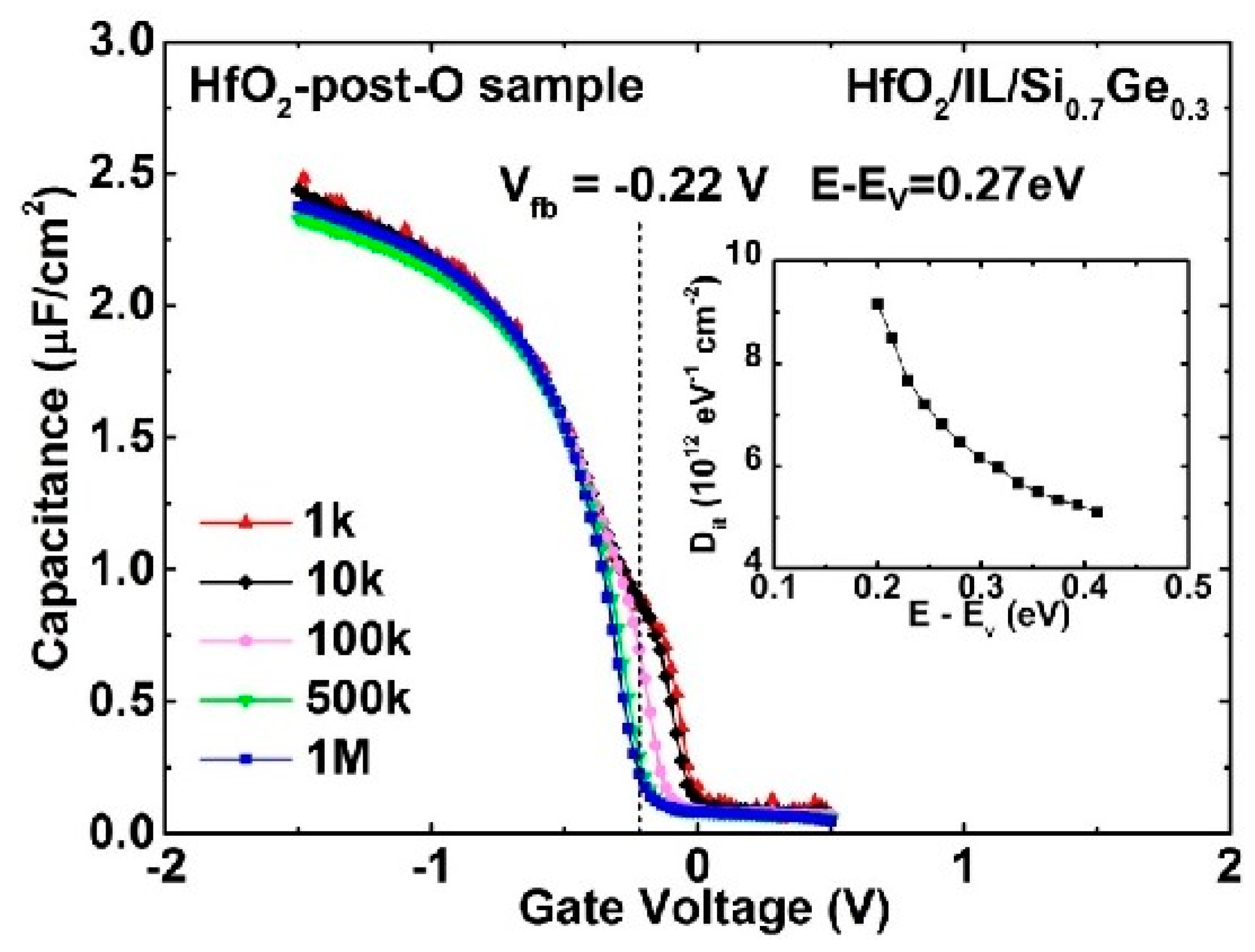
3.1. Low-Temperature Ozone Oxidation Passivation of HfO2/Si0.7Ge0.3 Interface
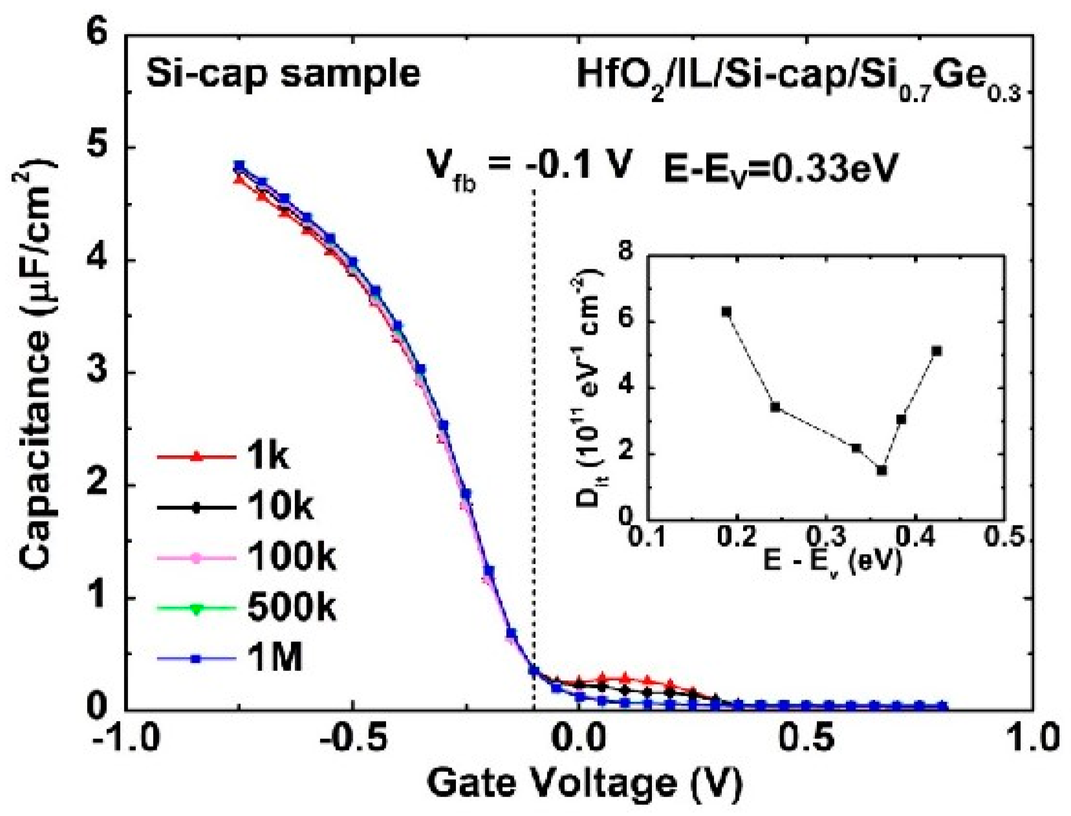
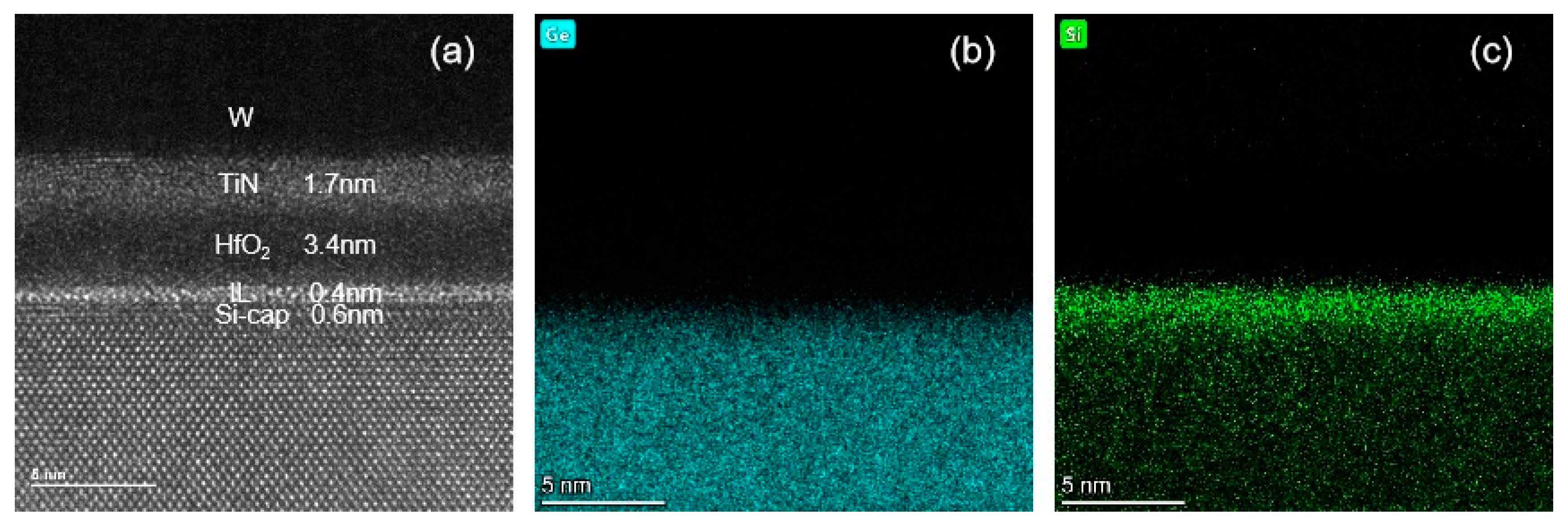
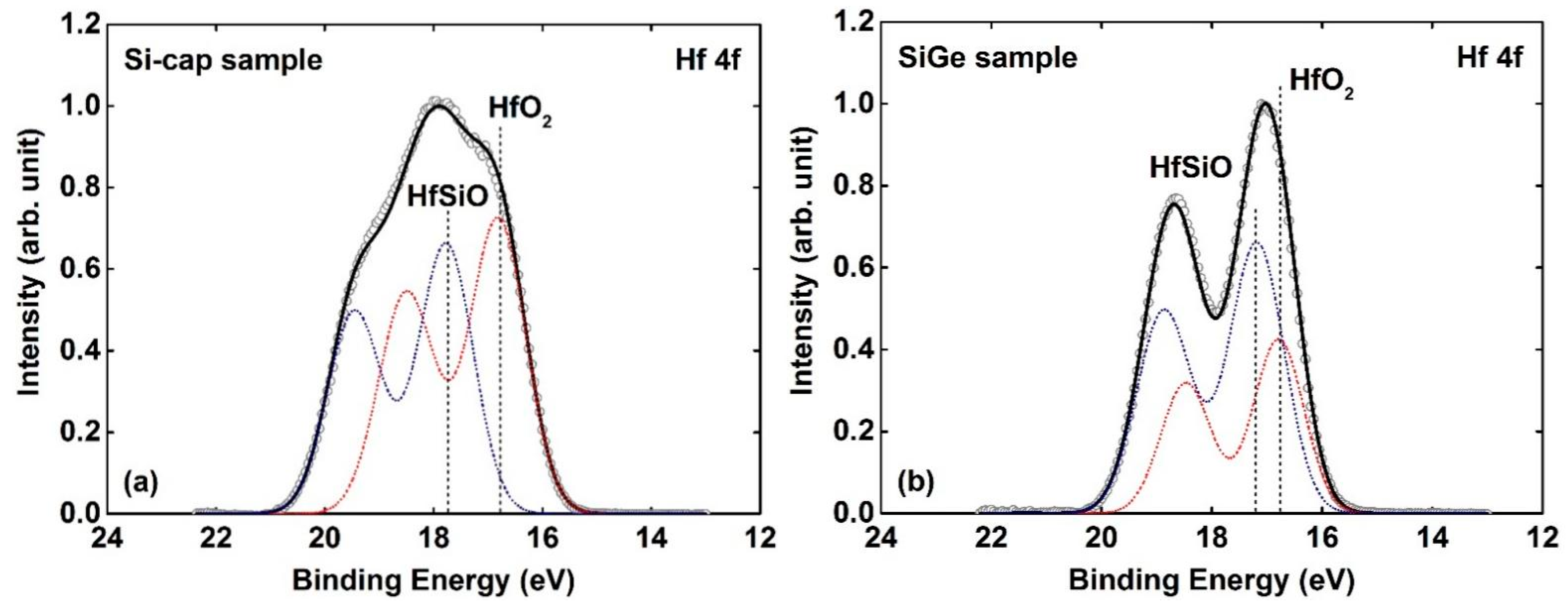
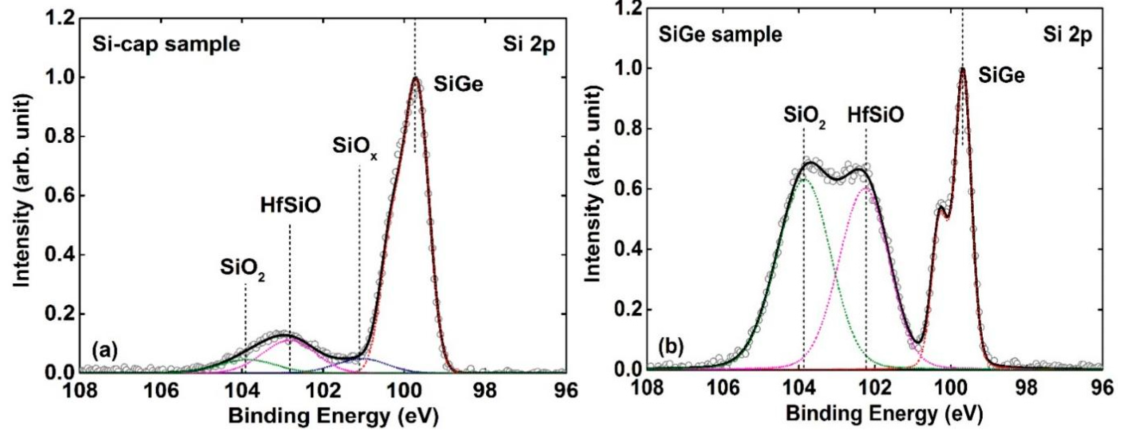
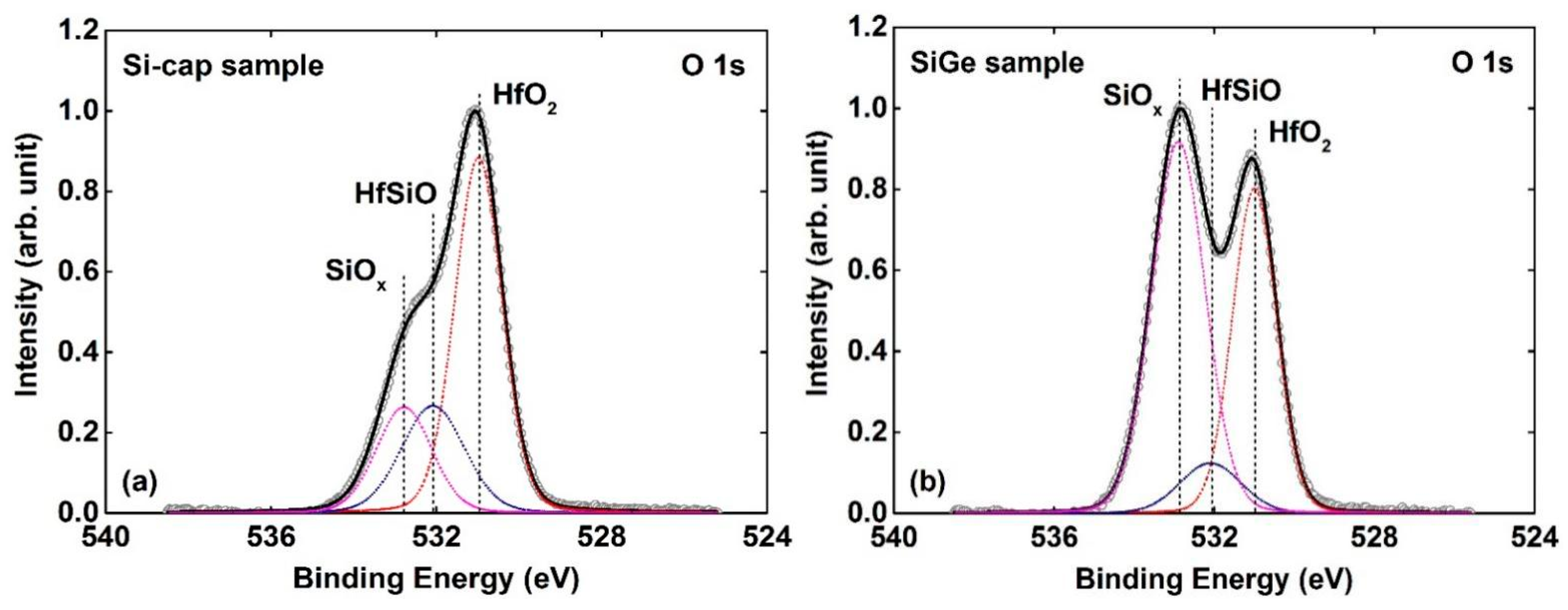
3.2. Si-Cap Passivation of HfO2/Si0.7Ge0.3 Interface
4. Conclusions
Author Contributions
Funding
Institutional Review Board Statement
Informed Consent Statement
Data Availability Statement
Acknowledgments
Conflicts of Interest
References
- Mertens, H.; Ritzenthaler, R.; Arimura, H.; Franco, J.; Sebaai, F.; Hikavyy, B.A.; Pawlak, J.; Machkaoutsan, V.; Devriendt, K.; Tsvetanova, D.; et al. Si-cap-free SiGe p-Channel FinFETsand Gate-All-Around Transistors in a Replacement Metal Gate Process: Interface Trap Density Reduction and Performance Improvement by High-Pressure Deuterium Anneal. In Proceedings of the 2015 Symposium on VLSI Technology, Kyoto, Japan, 16–18 June 2015. [Google Scholar]
- Hashemi, P.; Balakrishnan, K.; Engelmann, S.U.; Ott, J.A.; Khakifirooz, A.; Baraskar, A.; Hopstaken, M.; Newbury, J.S.; Chan, K.K.; Leobandung, E.; et al. First Demonstration of High-Ge-Content Strained-Si1-xGex(x = 0.5) on Insulator PMOS FinFETs with High Hole Mobility and Aggressively ScaledFin Dimensions and Gate Lengths for High-Performance Applications. In Proceedings of the 2014 IEEE International Electron Devices Meeting, San Francisco, CA, USA, 15–17 December 2014. [Google Scholar]
- Hashemi, P.; Ando, T.; Balakrishnan, K.; Bruley, J.; Engelmann, S.; Ott, J.A.; Narayanan, V.; Park, D.-G.; Mo, R.T.; and Leobandung, E. High-Mobility High-Ge-Content Si1-xGex-OI PMOS FinFETs with Fins Formed Using 3D Germanium Condensation with Ge Fraction up to x∼0.7, Scaled EOT∼8.5Å and ∼10nm Fin Width. In Proceedings of the 2015 Symposium on VLSI Circuits, Kyoto, Japan, 17–19 June 2015. [Google Scholar]
- Han, J.; Zhang, R.; Osada, T.; Hata, M.; Takenaka, M.; Takagi, S. Impact of plasma post-nitridation on HfO2/Al2O3/SiGe gate stacks toward EOT scaling. Microelectron. Eng. 2013, 109, 266–269. [Google Scholar] [CrossRef]
- Sardashti, K.; Hu, K.-T.; Tang, K.; Madisetti, S.; McIntyre, P.; Oktyabrsky, S.; Siddiqui, S.; Sahu, B.; Yoshida, N.; Kachian, J.; et al. Nitride passivation of the interface between high-k dielectrics and SiGe. Appl. Phys. Lett. 2016, 108, 011604. [Google Scholar] [CrossRef]
- Sardashtia, K.; Hua, K.T.; Tang, K.; Parka, S.; Kim, H.; Madisetti, S.; Oktyabrsky, S.; Siddiqui, S.; Sahu, B.; Yoshida, N.; et al. Sulfur passivation for the formation of Si-terminated Al2O3/SiGe(0 0 1) interfaces. Appl. Surf. Sci. 2016, 366, 455–463. [Google Scholar] [CrossRef]
- Hellberg, P.-E.; Zhang, S.-L.; d’Heurle, F.M.; Petersso, C.S. Oxidation of silicon–germanium alloys. I. An experimental study. J. Appl. Phys. 1997, 82, 5773–5778. [Google Scholar]
- Masanori, T.; Tatsuo, O.; Taizoh, S.; Miyao, M. Comprehensive study of low temperature (<1000 °C) oxidation process in SiGe/SOI structures. Thin Solid Films 2008, 517, 251–253. [Google Scholar]
- Song, Y.J.; Mheen, B.; Kang, J.Y.; Lee, Y.S.; Lee, N.E.; Kim, J.H.; Song, J.I.; Shim, K.-H. A low-temperature and high-quality radical-assisted oxidation process utilizing a remote ultraviolet ozone source for high-performance SiGe/Si MOSFETs. Semicond. Sci. Technol. 2004, 19, 792–797. [Google Scholar] [CrossRef]
- Ando, T.; Hashemi, P.; Bruley, J.; Rozen, J.; Ogawa, Y.; Koswatta, S.; Chan, K.K.; Cartier, E.A.; Mo, R.; Narayanan, V. High Mobility High-Ge-Content SiGe PMOSFETs Using Al2O3/HfO2 Stacks with In-Situ O3 Treatment. IEEE Electron. Device Lett. 2017, 38, 303–305. [Google Scholar] [CrossRef]
- Ma, X.L.; Xiang, J.J.; Zhou, L.X.; Wang, X.L.; Li, Y.L.; Yang, H.; Zhang, J.; Zhao, C.; Yin, H.X.; Wang, W.W.; et al. Comprehensive Study and Design of High-k/SiGe Gate Stacks with Interface-Engineering by Ozone Oxidation. ECS J. Solid-State Sci. Technol 2019, 8, N100–N105. [Google Scholar] [CrossRef]
- Ma, X.L.; Xiang, J.J.; Zhou, L.X.; Xu, H.; Wang, X.L.; Yang, H.; Li, Y.L.; Yin, H.X.; Wang, W.W. Understanding mechanisms impacting interface states of ozone-treated high-k/SiGe interfaces. Semicond. Sci. Technol. 2020, 35, 055018. [Google Scholar] [CrossRef]
- Yeh, W.K.; Chen, Y.T.; Huang, F.S.; Hsu, C.W.; Chen, C.Y.; Fang, Y.K.; Gan, K.J.; Chen, P.Y. The Improvement of High-k/Metal Gate pMOSFET Performance and Reliability Using Optimized Si Cap/SiGe Channel Structure. IEEE Trans. Device Mater. Reliab. 2011, 11, 7–12. [Google Scholar] [CrossRef]
- Tsutsui, G.; Durfee, C.; Wang, M.M.; Konar, A.; Wu, H.; Mochizuki, S.; Bao, R.Q.; Bedell, S.; Li, J.T.; Zhou, H.M.; et al. Leakage Aware Si/SiGe CMOS FinFET for Low Power Applications. In Proceedings of the 2008 IEEE Symposium on VLSI Technology, Honolulu, HI, USA, 18–22 June 2018. [Google Scholar]
- Ma, X.L.; Zhou, L.X.; Xiang, J.J.; Yang, H.; Wang, X.L.; Li, Y.L.; Zhang, J.; Zhao, C.; Yin, H.X.; Wang, W.W.; et al. Identification of a suitable passivation route for high-k/SiGe interface based on ozone oxidation. Appl. Surf. Sci. 2019, 493, 478–484. [Google Scholar] [CrossRef]
- Nicollian, E.H.; Brews, J.R. MOS (Metal Oxide Semiconductor) Physicsand Technology; John Wiley & Sons Inc.: Hoboken, NJ, USA, 1982; p. 176. [Google Scholar]
- Ma, X.L.; Wang, X.L.; Zhou, L.X.; Xu, H.; Zhang, Y.Y.; Duan, J.H.; Xiang, J.J.; Yang, H.; Li, J.J.; Li, Y.L.; et al. Experimental study of the ultrathin oxides on SiGe alloy formed by low-temperature ozone oxidation. Mater. Sci. Semicond. Process. 2020, 107, 104832. [Google Scholar] [CrossRef]
- Gusev, E.P.; Shang, H.; Copel, M.; Gribelyuk, M.; D’Emic, C.; Kozlowski, P.; Zabel, T.; Gusev, E.P.; Shang, H.; Copel, M.; et al. Microstructure and thermal stability of HfO2 gate dielectric deposited on Ge(100). Appl. Phys. Lett. 2004, 85, 2334. [Google Scholar] [CrossRef]
- Chang, C.T.; Toriumi, A. Preferential Oxidation of Si in SiGe for Shaping Ge-Rich SiGe Gate Stacks. In Proceedings of the 2015 IEEE International Electron Devices Meeting (IEDM), Washington, DC, USA, 7–9 December 2015. [Google Scholar]
- Shirley, D.A. High-Resolution X-ray Photoemission Spectrumof the Valence Bands of Gold. Phys. Review B 1972, 5, 4709. [Google Scholar] [CrossRef]


Publisher’s Note: MDPI stays neutral with regard to jurisdictional claims in published maps and institutional affiliations. |
© 2021 by the authors. Licensee MDPI, Basel, Switzerland. This article is an open access article distributed under the terms and conditions of the Creative Commons Attribution (CC BY) license (https://creativecommons.org/licenses/by/4.0/).
Share and Cite
Yao, Q.; Ma, X.; Wang, H.; Wang, Y.; Wang, G.; Zhang, J.; Liu, W.; Wang, X.; Yan, J.; Li, Y.; et al. Investigate on the Mechanism of HfO2/Si0.7Ge0.3 Interface Passivation Based on Low-Temperature Ozone Oxidation and Si-Cap Methods. Nanomaterials 2021, 11, 955. https://doi.org/10.3390/nano11040955
Yao Q, Ma X, Wang H, Wang Y, Wang G, Zhang J, Liu W, Wang X, Yan J, Li Y, et al. Investigate on the Mechanism of HfO2/Si0.7Ge0.3 Interface Passivation Based on Low-Temperature Ozone Oxidation and Si-Cap Methods. Nanomaterials. 2021; 11(4):955. https://doi.org/10.3390/nano11040955
Chicago/Turabian StyleYao, Qide, Xueli Ma, Hanxiang Wang, Yanrong Wang, Guilei Wang, Jing Zhang, Wenkai Liu, Xiaolei Wang, Jiang Yan, Yongliang Li, and et al. 2021. "Investigate on the Mechanism of HfO2/Si0.7Ge0.3 Interface Passivation Based on Low-Temperature Ozone Oxidation and Si-Cap Methods" Nanomaterials 11, no. 4: 955. https://doi.org/10.3390/nano11040955
APA StyleYao, Q., Ma, X., Wang, H., Wang, Y., Wang, G., Zhang, J., Liu, W., Wang, X., Yan, J., Li, Y., & Wang, W. (2021). Investigate on the Mechanism of HfO2/Si0.7Ge0.3 Interface Passivation Based on Low-Temperature Ozone Oxidation and Si-Cap Methods. Nanomaterials, 11(4), 955. https://doi.org/10.3390/nano11040955