
High Performance p-i-n Photodetectors on Ge-on-Insulator Platform

 ,
,  , , , ,
Abstract
1. Introduction
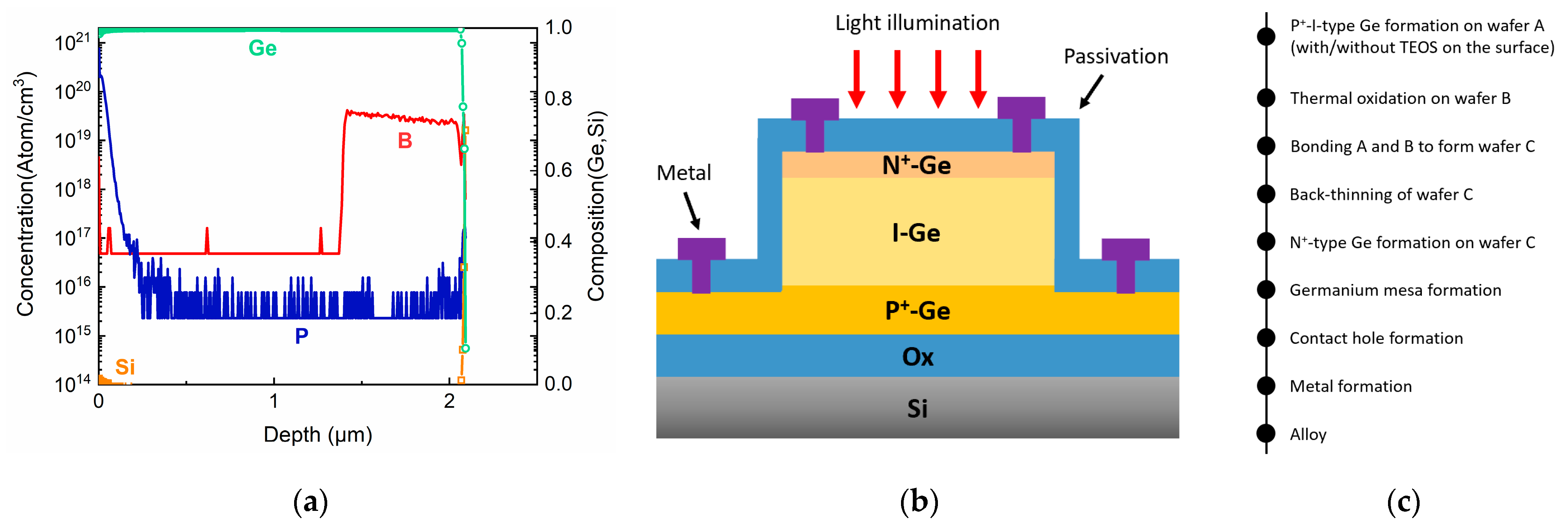
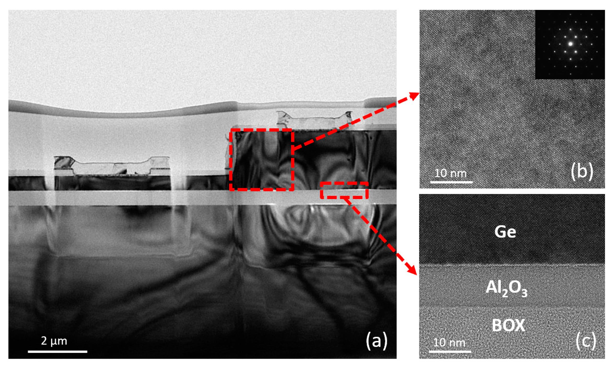
2. Materials and Methods
3. Results and Discussions
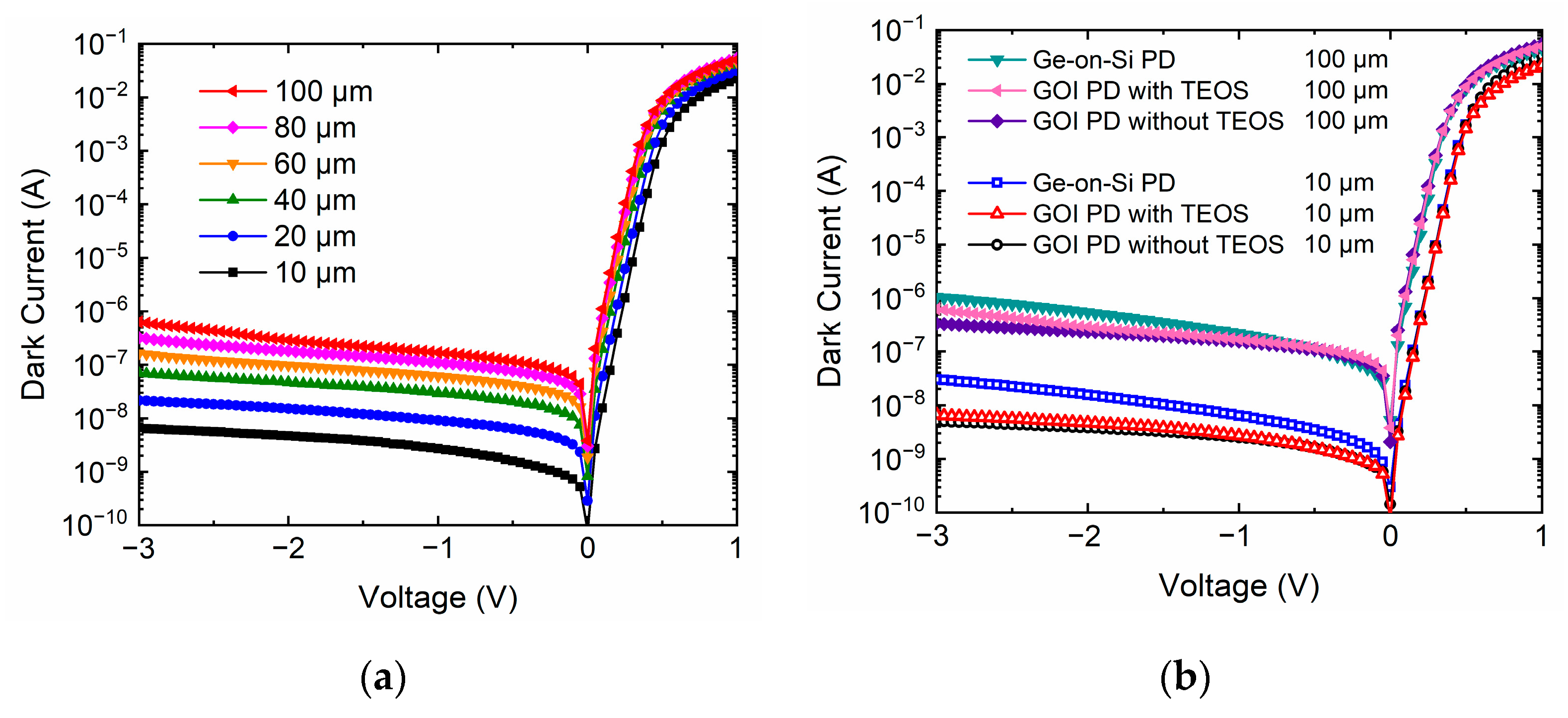
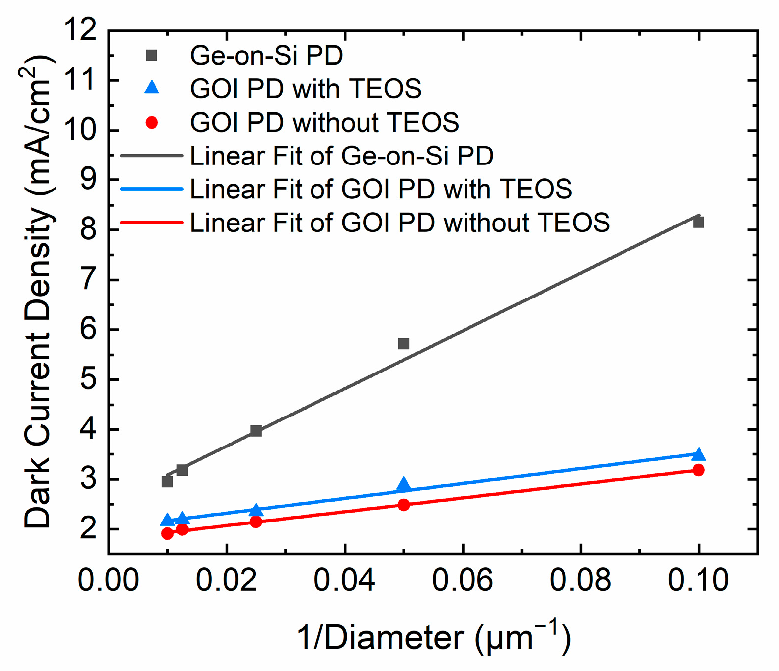
3.1. Dark Current
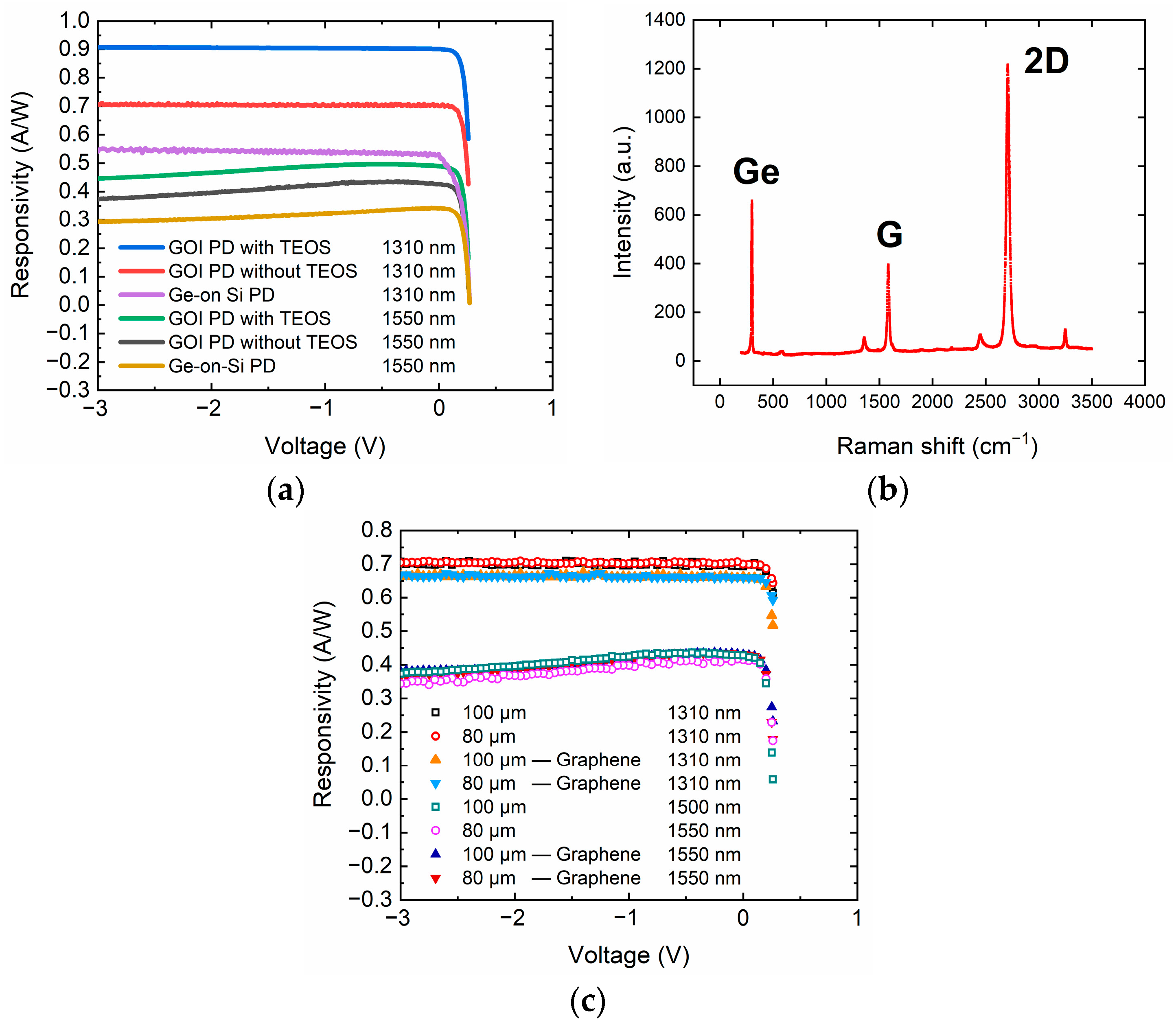
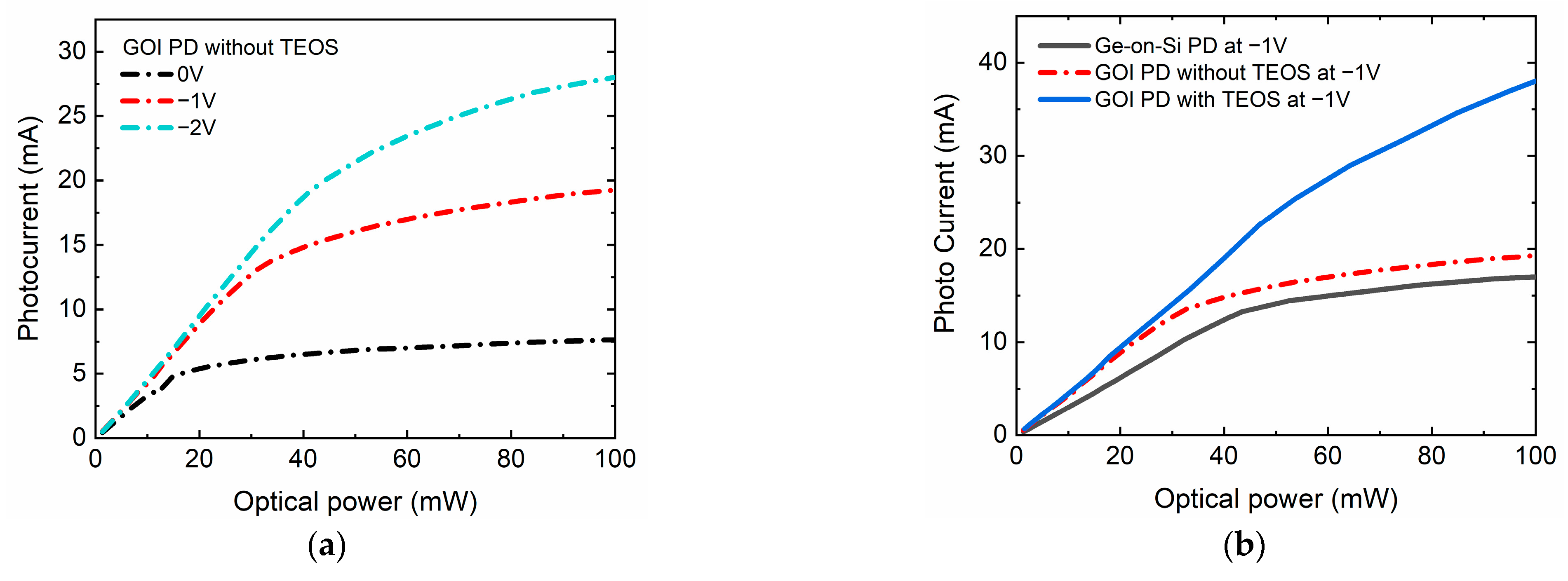
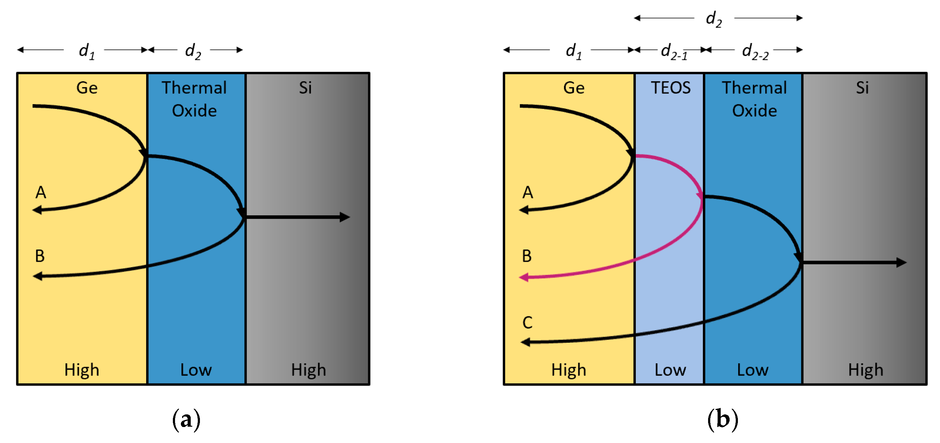
3.2. Responsivity
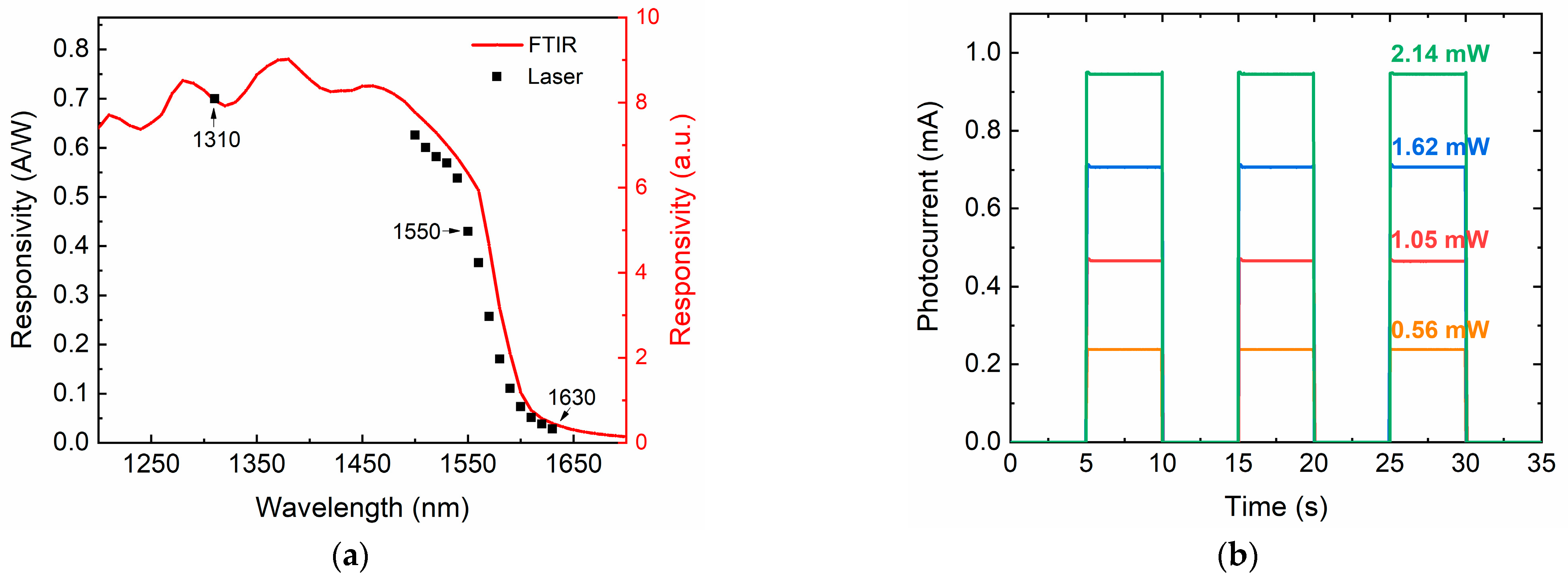
3.3. Spectral Response
4. Conclusions
5. Patents
Author Contributions
Funding
Data Availability Statement
Conflicts of Interest
References
- Radamson, H.H.; Zhu, H.; Wu, Z.; He, X.; Lin, H.; Liu, J.; Xiang, J.; Kong, Z.; Xiong, W.; Li, J.; et al. State of the Art and Future Perspectives in Advanced CMOS Technology. Nanomaterials 2020, 10, 1555. [Google Scholar] [CrossRef]
- Radamson, H.H.; Simeon, E.; Luo, J.; Wang, G. 2-Scaling and evolution of device architecture. In CMOS Past, Present and Future; Radamson, H.H., Luo, J., Simoen, E., Zhao, C., Eds.; Woodhead Publishing: Shaston, UK, 2018. [Google Scholar] [CrossRef]
- Michel, J.; Liu, J.; Kimerling, L.C. High-performance Ge-on-Si photodetectors. Nat. Photonics 2010, 4, 527–534. [Google Scholar] [CrossRef]
- Luryi, S.; Kastalsky, A.; Bean, J.C. New infrared detector on a silicon chip. IEEE Electron. Device Lett. 1984, 31, 1135–1139. [Google Scholar] [CrossRef]
- Colace, L.; Gianlorenzo, M.; Galluzzi, F.; Assanto, G.; Capellini, G.; Di Gaspare, L.; Evangelisti, F. Ge/Si (001) Photodetector for Near Infrared Light. Solid State Phenom. 1997, 54, 55–58. [Google Scholar] [CrossRef]
- Yu, H.; Ren, S.; Jung, W.S.; Okyay, A.K.; Miller, D.A.B.; Saraswat, K.C. High-Efficiency p-i-n Photodetectors on Selective-Area-Grown Ge for Monolithic Integration. IEEE Electron. Device Lett. 2009, 30, 1161–1163. [Google Scholar] [CrossRef]
- Huang, Z.; Kong, N.; Guo, X.; Liu, M.; Duan, N.; Beck, A.L.; Banerjee, S.K.; Campbell, J.C. 21-GHz-Bandwidth Germanium-on-Silicon Photodiode Using Thin SiGe Buffer Layers. IEEE J. Sel. Top. Quantum Electron. 2006, 12, 1450–1454. [Google Scholar] [CrossRef]
- Radamson, H.; Thylén, L. Chapter 3—Silicon and Group IV Photonics. In Monolithic Nanoscale Photonics–Electronics Integration in Silicon and Other Group IV Elements; Radamson, H., Thylén, L., Eds.; Academic Press: Oxford, UK, 2015; pp. 87–119. [Google Scholar] [CrossRef]
- Ni, W.X.; Ekberg, J.O.; Joelsson, K.B.; Radamson, H.; Henry, A.; Shen, G.D.; Hansson, G. A silicon molecular beam epitaxy system dedicated to device-oriented material research. J. Cryst. Growth 1995, 157, 285–294. [Google Scholar] [CrossRef]
- Zhou, Z.; He, J.; Wang, R.; Li, C.; Yu, J. Normal incidence p–i–n Ge heterojunction photodiodes on Si substrate grown by ultrahigh vacuum chemical vapor deposition. Opt. Commun. 2010, 283, 3404–3407. [Google Scholar] [CrossRef]
- Li, C.; Xue, C.; Liu, Z.; Cheng, B.; Li, C.; Wang, Q. High-Bandwidth and High-Responsivity Top-Illuminated Germanium Photodiodes for Optical Interconnection. IEEE Electron. Device Lett. 2013, 60, 1183–1187. [Google Scholar] [CrossRef]
- Li, X.; Peng, L.; Liu, Z.; Liu, X.; Zheng, J.; Zuo, Y.; Xue, C.; Cheng, B. High-power back-to-back dual-absorption germanium photodetector. Opt Lett. 2020, 45, 1358–1361. [Google Scholar] [CrossRef]
- Fang, Q.; Jia, L.; Song, J.; Lim, A.E.; Tu, X.; Luo, X.; Yu, M.; Lo, G. Demonstration of a vertical pin Ge-on-Si photo-detector on a wet-etched Si recess. Opt Express 2013, 21, 23325–23330. [Google Scholar] [CrossRef]
- Chen, H.; Verheyen, P.; De Heyn, P.; Lepage, G.; De Coster, J.; Balakrishnan, S.; Absil, P.; Yao, W.; Shen, L.; Roelkens, G.; et al. −1 V bias 67 GHz bandwidth Si-contacted germanium waveguide p-i-n photodetector for optical links at 56 Gbps and beyond. Opt. Express. 2016, 24, 4622–4631. [Google Scholar] [CrossRef]
- Okyay, A.K.; Nayfeh, A.M.; Saraswat, K.C.; Yonehara, T.; Marshall, A.; McIntyre, P.C. High-efficiency metal-semiconductor-metal photodetectors on heteroepitaxially grown Ge on Si. Opt. Lett. 2006, 31, 2565–2567. [Google Scholar] [CrossRef]
- Lee, K.H.; Bao, S.; Chong, G.Y.; Tan, Y.H.; Fitzgerald, E.A.; Tan, C.S. Defects reduction of Ge epitaxial film in a germanium-on-insulator wafer by annealing in oxygen ambient. Appl. Mater. 2015, 3. [Google Scholar] [CrossRef]
- Son, B.; Lin, Y.; Lee, K.H.; Chen, Q.; Tan, C.S. Dark current analysis of germanium-on-insulator vertical p-i-n photodetectors with varying threading dislocation density. Int. J. Appl. Phys. 2020, 127. [Google Scholar] [CrossRef]
- Ghosh, S.; Lin, K.C.; Tsai, C.H.; Lee, K.H.; Chen, Q.; Son, B.; Mukhopadhyay, B.; Tan, C.S.; Chang, G.E. Resonant-cavity-enhanced responsivity in germanium-on-insulator photodetectors. Opt Express 2020, 28, 23739–23747. [Google Scholar] [CrossRef] [PubMed]
- Radamson, H.H.; Noroozi, M.; Jamshidi, A.; Thompson, P.E.; Ostling, M. Strain Engineering in GeSnSi Materials. Ecs Trans. 2013, 50, 527–531. [Google Scholar] [CrossRef]
- Fang, Y.; Tolle, J.; Roucka, R.; Chizmeshya, A.; Kouvetakis, J.; D’Costa, V.; Menendez, J. Perfectly tetragonal, tensile-strained Ge on Ge1−ySny buffered Si(100). Appl. Phys. Lett. 2007, 90, 061915. [Google Scholar] [CrossRef]
- Sanchez-Perez, J.R.; Boztug, C.; Chen, F.; Sudradjat, F.F.; Paskiewicz, D.M.; Jacobson, R.; Lagally, M.G.; Paiella, R. Direct-bandgap light-emitting germanium in tensilely strained nanomembranes. Proc. Natl. Acad. Sci. USA 2011, 108, 18893–18898. [Google Scholar] [CrossRef] [PubMed]
- Bao, S.; Kim, D.; Onwukaeme, C.; Gupta, S.; Saraswat, K.; Lee, K.H.; Kim, Y.; Min, D.; Jung, Y.; Qiu, H.; et al. Low-threshold optically pumped lasing in highly strained germanium nanowires. Nat. Commun. 2017, 8, 1845. [Google Scholar] [CrossRef] [PubMed]
- Ghrib, A.; El Kurdi, M.; Prost, M.; Sauvage, S.; Checoury, X.; Beaudoin, G.; Chaigneau, M.; Ossikovski, R.; Sagnes, I.; Boucaud, P. All-Around SiN Stressor for High and Homogeneous Tensile Strain in Germanium Microdisk Cavities. Adv. Opt. Mater. 2015, 3, 353–358. [Google Scholar] [CrossRef]
- Jain, J.R.; Hryciw, A.; Baer, T.M.; Miller, D.A.B.; Brongersma, M.L.; Howe, R.T. A micromachining-based technology for enhancing germanium light emission via tensile strain. Nat. Photonics 2012, 6, 398–405. [Google Scholar] [CrossRef]
- Nam, J.H.; Afshinmanesh, F.; Nam, D.; Jung, W.S.; Kamins, T.I.; Brongersma, M.L.; Saraswat, K.C. Monolithic integration of germanium-on-insulator p-i-n photodetector on silicon. Opt Express 2015, 23, 15816–15823. [Google Scholar] [CrossRef] [PubMed]
- Son, B.; Lin, Y.; Lee, K.H.; Wang, Y.; Wu, S.; Tan, C.S. High speed and ultra-low dark current Ge vertical p-i-n photodetectors on an oxygen-annealed Ge-on-insulator platform with GeOx surface passivation. Opt. Express 2020, 28, 23978–23990. [Google Scholar] [CrossRef] [PubMed]
- Lin, Y.; Lee, K.H.; Bao, S.; Guo, X.; Wang, H.; Michel, J.; Tan, C.S. High-efficiency normal-incidence vertical p-i-n photodetectors on a germanium-on-insulator platform. Photonics Res. 2017, 5. [Google Scholar] [CrossRef]
- Cheng, C.Y.; Tsai, C.H.; Yeh, P.L.; Hung, S.F.; Bao, S.; Lee, K.H.; Tan, C.S.; Chang, G.E. Ge-on-insulator lateral p-i-n waveguide photodetectors for optical communication. Opt. Lett. 2020, 45, 6683–6686. [Google Scholar] [CrossRef]
- Wang, X.; Xiang, J.; Han, K.; Wang, S.; Luo, J.; Zhao, C.; Ye, T.; Radamson, H.H.; Simoen, E.; Wang, W. Physically Based Evaluation of Effect of Buried Oxide on Surface Roughness Scattering Limited Hole Mobility in Ultrathin GeOI MOSFETs. IEEE Electron. Device Lett. 2017, 64, 2611–2616. [Google Scholar] [CrossRef]
- Radamson, H.; Joelsson, K.; Ni, W.X.; Hultman, L.; Hansson, G. Characterization of highly boron-doped Si, Si 1 − x Ge x and Ge layers by high-resolution transmission electron microscopy. J. Cryst. Growth 1995, 157, 80–84. [Google Scholar] [CrossRef]
- Hållstedt, J.; Blomqvist, M.; Persson, P.; Hultman, L.; Radamson, H. The effect of carbon and germanium on phase transformation of nickel on Si1-x-yGexCy epitaxial layers. Int. J. Appl. Phys. 2004, 95, 2397–2402. [Google Scholar] [CrossRef]
- Nur, O.; Willander, M.; Radamson, H.H.; Sardela, M.R.; Hansson, G.V.; Petersson, C.S.; Maex, K. Strain characterization of CoSi2/n-Si0.9Ge0.1/p-Si heterostructures. Int. J. Appl. Phys. 1994, 64, 440–442. [Google Scholar] [CrossRef]
- Nur, O.; Willander, M.; Hultman, L.; Radamson, H.; Hansson, G.; Sardela, M.; Greene, J. CoSi2/Si1-xGex/Si(001) heterostructures formed through different reaction routes: Silicidation-induced strain relaxation, defect formation, and interlayer diffusionInt. J. Appl. Phys. 1996, 78, 7063–7069. [Google Scholar] [CrossRef]
- Eneman, G.; Gonzalez, M.; Hellings, G.; Jaeger, B.; Wang, G.; Mitard, J.; DeMeyer, K.; Claeys, C.; Meuris, M.; Heyns, M.; et al. Trap-Assisted Tunneling in Deep-Submicron Ge pFET Junctions. ECS Trans. 2010, 28, 143–152. [Google Scholar] [CrossRef]
- Colace, L.; Assanto, G.; Fulgoni, D.; Nash, L. Near-Infrared p-i-n Ge-on-Si Photodiodes for Silicon Integrated Receivers. J. Light. Technol. 2008, 26, 2954–2959. [Google Scholar] [CrossRef]
- Liu, Z.; Yang, F.; Wu, W.; Cong, H.; Zheng, J.; Li, C.; Xue, C.; Cheng, B.; Wang, Q. 48 GHz High-Performance Ge-on-SOI Photodetector With Zero-Bias 40 Gbps Grown by Selective Epitaxial Growth. J. Light. Technol. 2017, 35, 5306–5310. [Google Scholar] [CrossRef]
- Schmid, M.; Kaschel, M.; Gollhofer, M.; Oehme, M.; Werner, J.; Kasper, E.; Schulze, J. Franz–Keldysh effect of germanium-on-silicon p–i–n diodes within a wide temperature range. Thin Solid Films 2012, 525, 110–114. [Google Scholar] [CrossRef]
- Kasap, S.; Sinha, R. Optoelectronics and Photonics: Principles and Practice, 2nd ed.; University of Saskatchewan: Saskatoon, SK, Canada, 2013. [Google Scholar]
- Liu, J.; Michel, J.; Giziewicz, W.; Pan, D.; Wada, K.; Cannon, D.; Jongthammanurak, S.; Danielson, D.; Kimerling, L.; Chen, J.; et al. High-performance, tensile-strained Ge p-i-n photodetectors on a Si platform. Appl. Phys. Lett. 2005, 87, 103501. [Google Scholar] [CrossRef]
- Klinger, S.; Berroth, M.; Kaschel, M.; Oehme, M.; Kasper, E. Ge-on-Si p-i-n Photodiodes With a 3-dB Bandwidth of 49 GHz. IEEE Photonics Technol. Lett. 2009, 21, 920–922. [Google Scholar] [CrossRef]
- Zhao, X.; Moeen, M.; Toprak, M.S.; Wang, G.; Luo, J.; Ke, X.; Li, Z.; Liu, D.; Wang, W.; Zhao, C.; et al. Design impact on the performance of Ge PIN photodetectors. J. Mater. Sci. Mater. Electron. 2019, 31, 18–25. [Google Scholar] [CrossRef]


| Dark Current Density | Ge-on-Si PD | GOI PD with TEOS | GOI PD without TEOS |
|---|---|---|---|
| Jbulk (mA/cm2) | 2.50 | 2.02 | 1.79 |
| Jsurf (μA/cm) | 1.45 | 0.37 | 0.34 |
| GOI | Oxide Thickness | ||
|---|---|---|---|
| m value | 1 | 2 | 3 |
| effect | Constructive | Destructive | Constructive |
| 1550 nm | 267 nm | 534 nm | 801 nm |
| 1310 nm | 226 nm | 452 nm | 678 nm |
| Year | Active Area (μm2) | Dark Current at −1 V (nA) | Dark Current Density at −1 V (mA/cm2) | Responsivity at 1550 nm (A/W) | Responsivity at 1310 nm (A/W) | Quantum Efficiency (1550 nm/1310 nm) | Ref |
|---|---|---|---|---|---|---|---|
| 2005 | π × 2500 | 1728 at −2 V * | 22 at −2 V | 0.56 at −2 V | 0.87 at −2 V | 45%/82% * | [39] |
| 2008 | 20 × 20 | 6.8 * | 1.7 | 0.2 at −1 V | 0.3 at −1 V | 16%/28% * | [35] |
| 2009 | π × 25 | 102 * | 130 | 0.05 at −2 V | 0.2 at −2 V | 4%/19% * | [40] |
| 2010 | 50 × 50 | 990 | 40 | 0.13 at −1 V | —— | 10.4%/— | [10] |
| 2013 | π ×100 | 120 * | 38.3 | 0.30 at −1 V | —— | 24%/— | [11] |
| 2017 | π × 36 | 5.2 | 4.6 | 0.27 at 0 V | 0.59 at 0 V | 21.6%/55.8% | [36] |
| 2017 | π × 900 | 1329 * | 47 | 0.39 at −2 V | —— | 31.2%/— * | [27] GOI |
| 2019 | π × 25 | 4 | 5 | 0.12 at −1 V | —— | 10%/— * | [41] |
| 2020 | π × 56.25 | 450 | 255 * | 0.31 at −1 V | 0.52 at −1 V | 24.8%/49.2% | [12] |
| 2020 | π × 15625 | 280 * | 0.57 | 0.28 at −1 V | —— | 22.4%/— * | [26] GOI |
| This work | π × 25 | 6.4 | 8.1 | 0.32 at −1 V | 0.54 at −1 V | 25.6%/51.1% | Ge on Si |
| This work | π × 25 | 2.5 | 3.2 | 0.43 at −1 V | 0.70 at −1 V | 34.4%/66.3% | GOI WO-TEOS |
| This work | π × 25 | 2.7 | 3.4 | 0.50 at −1 V | 0.90 at −1 V | 40%/85.2% | GOI W-TEOS |
Publisher’s Note: MDPI stays neutral with regard to jurisdictional claims in published maps and institutional affiliations. |
© 2021 by the authors. Licensee MDPI, Basel, Switzerland. This article is an open access article distributed under the terms and conditions of the Creative Commons Attribution (CC BY) license (https://creativecommons.org/licenses/by/4.0/).
Share and Cite
Zhao, X.; Wang, G.; Lin, H.; Du, Y.; Luo, X.; Kong, Z.; Su, J.; Li, J.; Xiong, W.; Miao, Y.; et al. High Performance p-i-n Photodetectors on Ge-on-Insulator Platform. Nanomaterials 2021, 11, 1125. https://doi.org/10.3390/nano11051125
Zhao X, Wang G, Lin H, Du Y, Luo X, Kong Z, Su J, Li J, Xiong W, Miao Y, et al. High Performance p-i-n Photodetectors on Ge-on-Insulator Platform. Nanomaterials. 2021; 11(5):1125. https://doi.org/10.3390/nano11051125
Chicago/Turabian StyleZhao, Xuewei, Guilei Wang, Hongxiao Lin, Yong Du, Xue Luo, Zhenzhen Kong, Jiale Su, Junjie Li, Wenjuan Xiong, Yuanhao Miao, and et al. 2021. "High Performance p-i-n Photodetectors on Ge-on-Insulator Platform" Nanomaterials 11, no. 5: 1125. https://doi.org/10.3390/nano11051125
APA StyleZhao, X., Wang, G., Lin, H., Du, Y., Luo, X., Kong, Z., Su, J., Li, J., Xiong, W., Miao, Y., Li, H., Guo, G., & Radamson, H. H. (2021). High Performance p-i-n Photodetectors on Ge-on-Insulator Platform. Nanomaterials, 11(5), 1125. https://doi.org/10.3390/nano11051125