
Laser-Induced Transfer of Noble Metal Nanodots with Femtosecond Laser-Interference Processing

 ,
,
Abstract
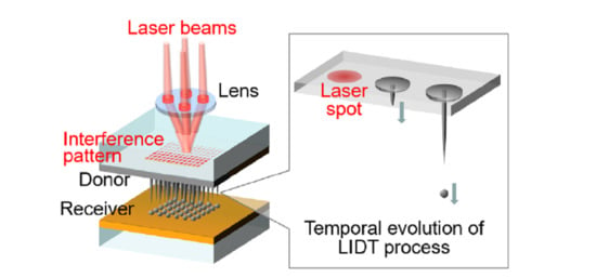
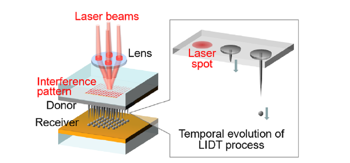
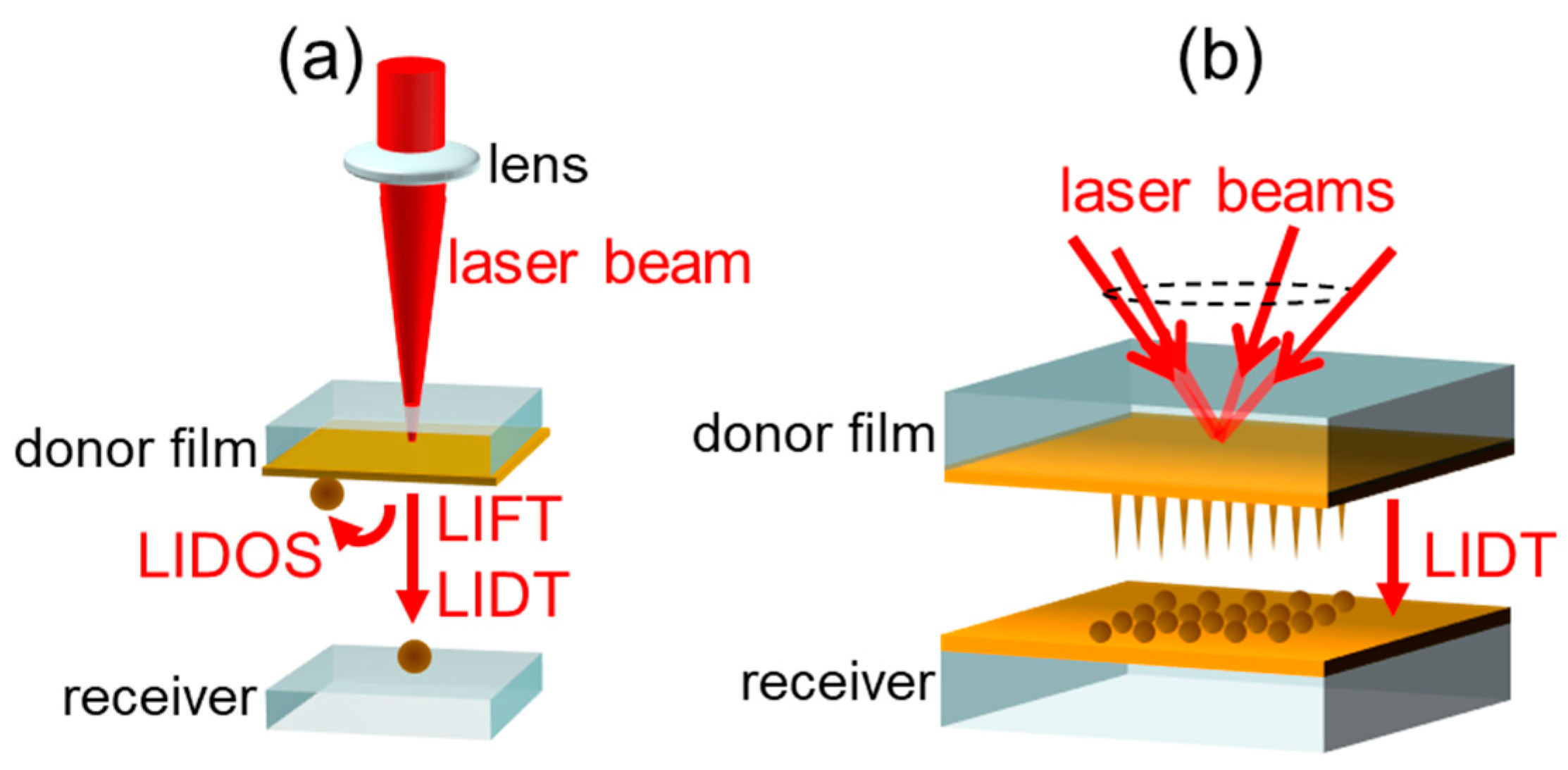
1. Introduction
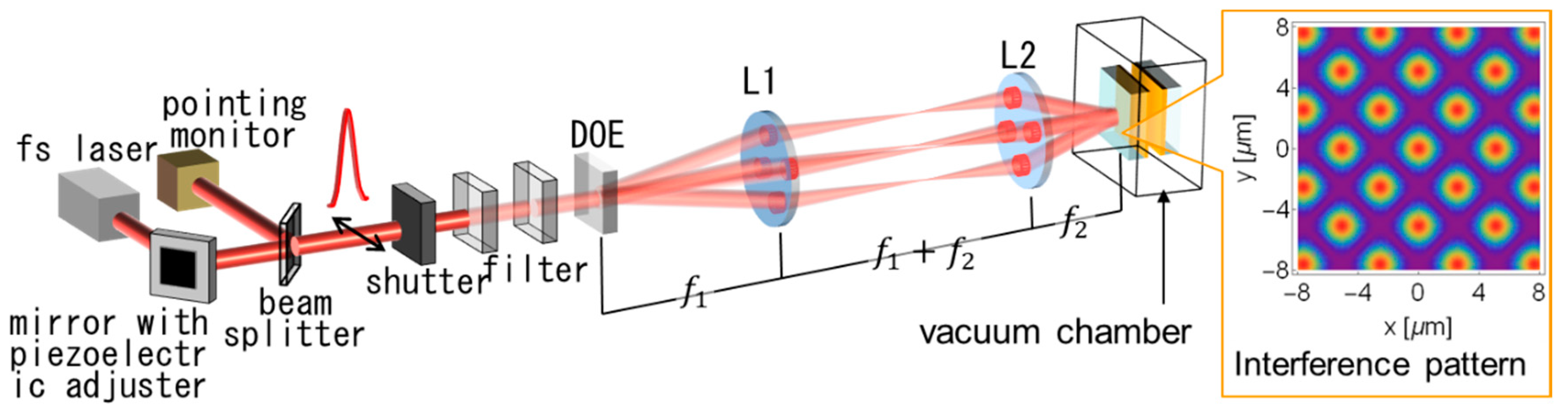
2. Materials and Methods
3. Results and Discussion
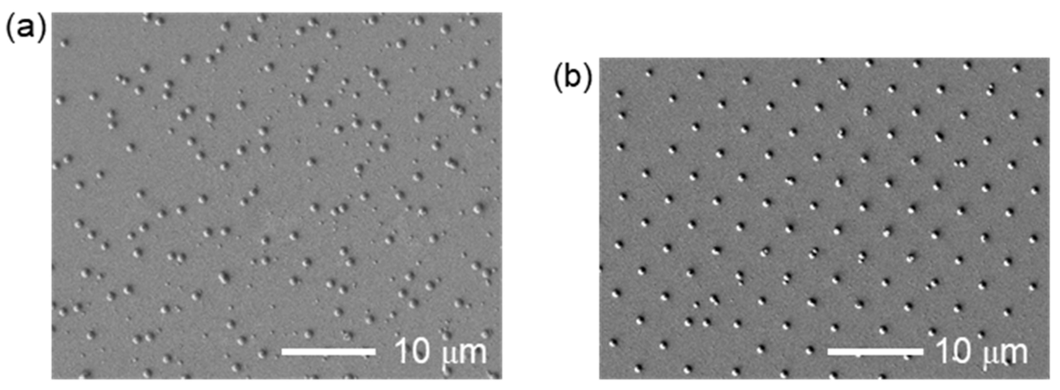
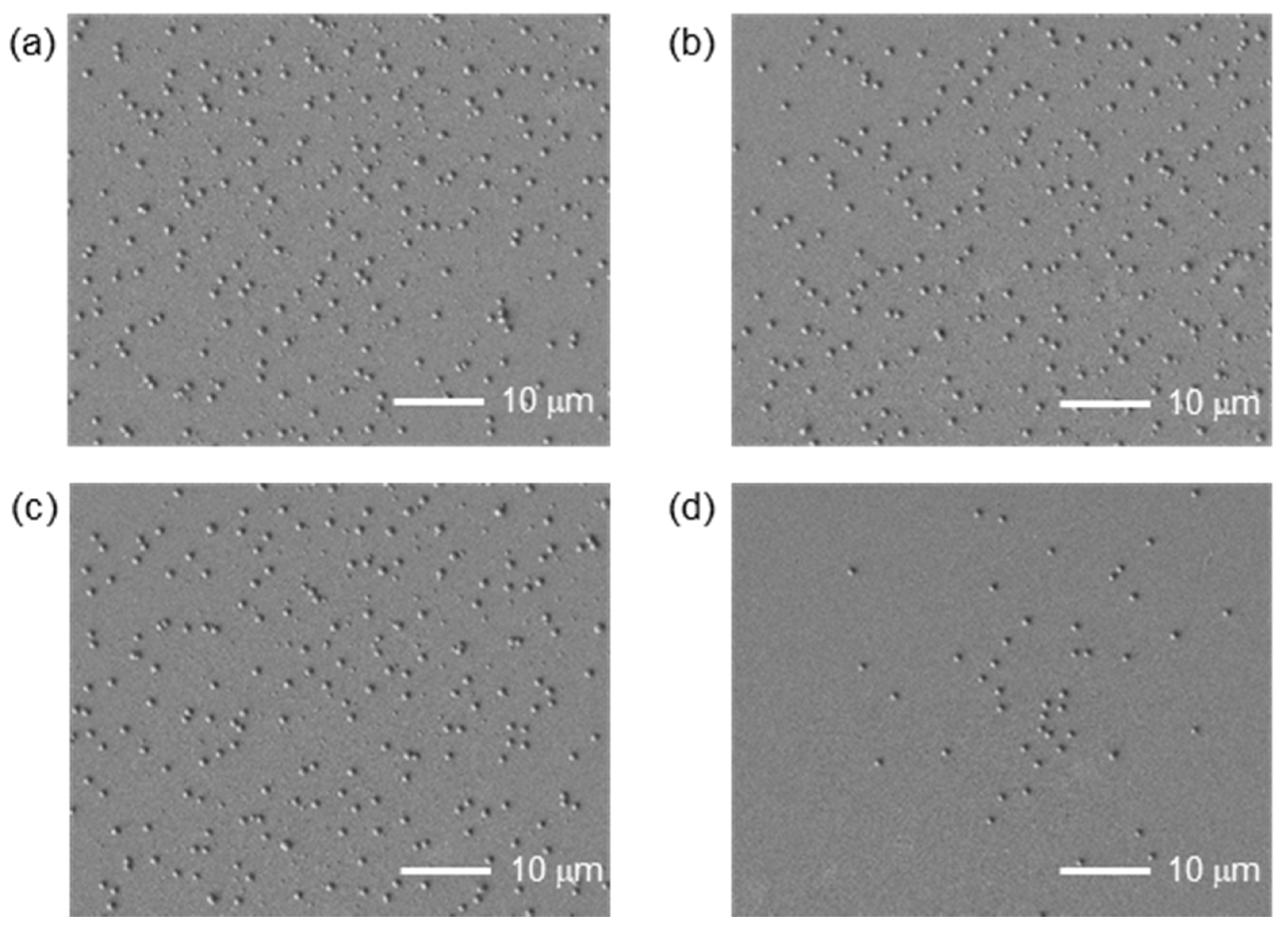
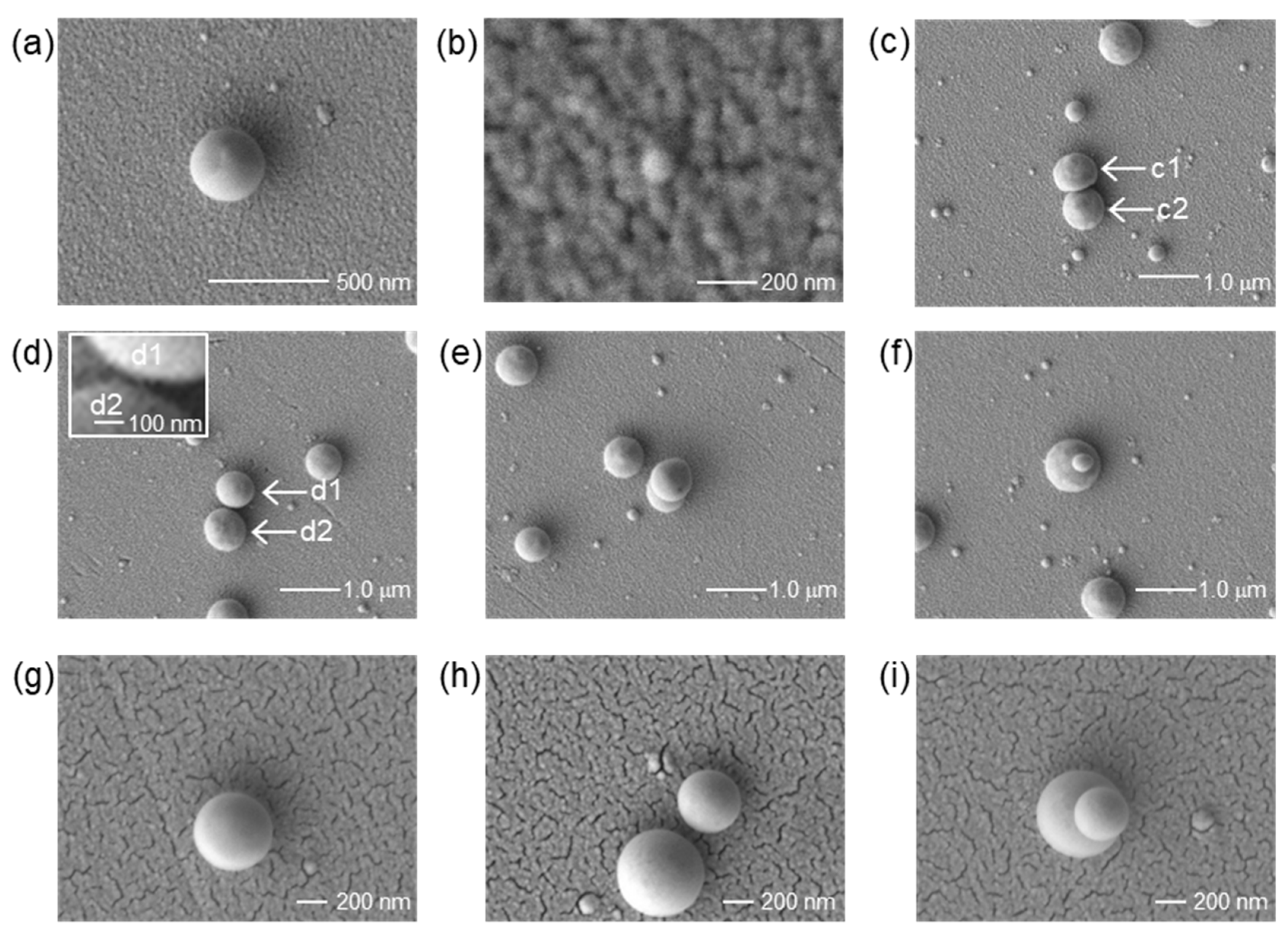
3.1. SEM Images of the Pt Nanodots
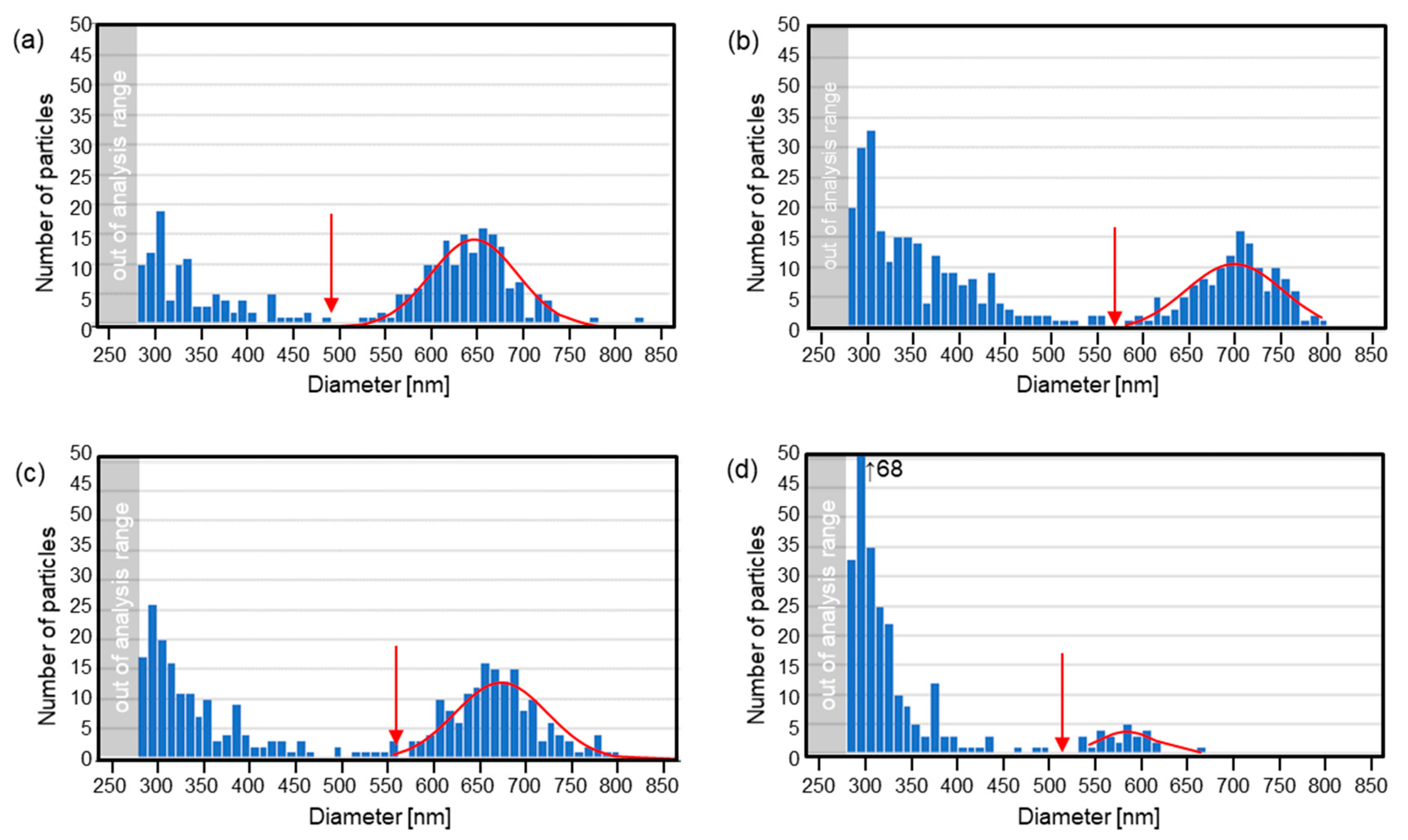
3.2. Statistical Analysis
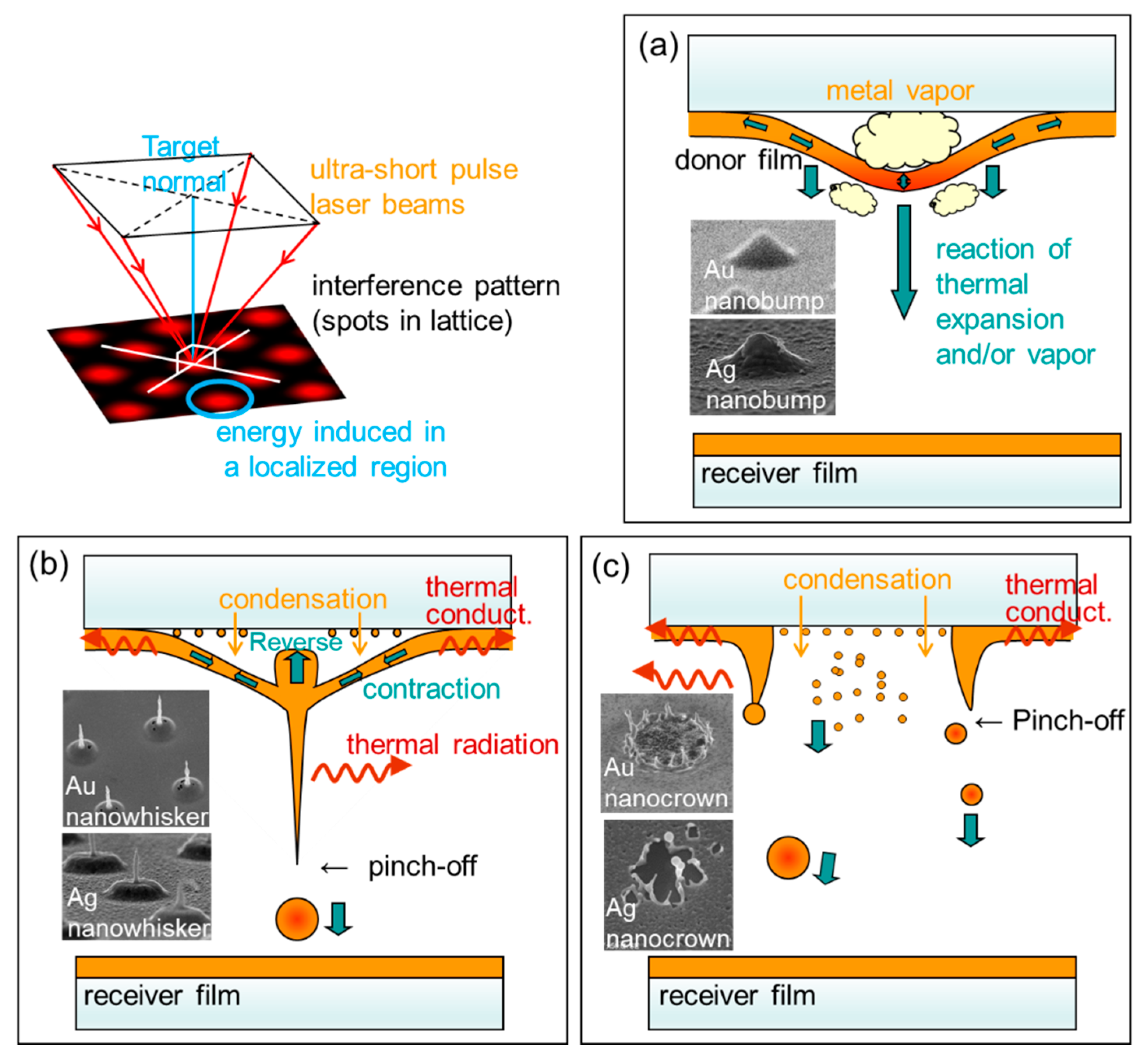
3.3. Heuristic Model of LIDT
4. Conclusions
Author Contributions
Funding
Conflicts of Interest
References
- Levene, M.L.; Scott, R.D.; Siryj, B.W. Material Transfer Recording. Appl. Opt. 1970, 9, 2260–2265. [Google Scholar] [CrossRef] [PubMed]
- Bohandy, J. Metal deposition from a supported metal film using an excimer laser. J. Appl. Phys. 1986, 60, 10–12. [Google Scholar] [CrossRef]
- Piqué, A.; Chrisey, D.B.; Auyeung, R.C.Y.; Fitz-Gerald, J.; Wu, H.D.; McGill, R.A.; Lakeou, S.; Wu, P.K.; Nguyen, V.; Duignan, M. A novel laser transfer process for direct writing of electronic and sensor materials. Appl. Phys. A Mater. Sci. Process. 1999, 69, 279–284. [Google Scholar] [CrossRef]
- Colina, M.; Serra, P.; Fernández-Pradas, J.M.; Sevilla, L.; Morenza, J.L. DNA deposition through laser induced forward transfer. Biosens. Bioelectron. 2005, 20, 1638–1642. [Google Scholar] [CrossRef] [PubMed]
- Nakata, Y.; Okada, T.; Maeda, M. Transfer of Laser Dye by Laser-Induced Forward Transfer. Jpn. J. Appl. Phys. 2002, 41, L839–L841. [Google Scholar] [CrossRef]
- Nakata, Y.; Okada, T. Time-resolved microscopic imaging of the laser-induced forward transfer process. Appl. Phys. A Mater. Sci. Process. 1999, 69, S275–S278. [Google Scholar] [CrossRef]
- Nakata, Y.; Okada, T.; Maeda, M. Application and observation of laser-induced forward transfer process. Proc. SPIE 2002, 4637, 435–444. [Google Scholar] [CrossRef]
- Narazaki, A.; Sato, T.; Kurosaki, R.; Kawaguchi, Y.; Niino, H. Nano- and microdot array formation of FeSi2 by nanosecond excimer laser-induced forward transfer. Appl. Phys. Express 2008, 1, 0570011–0570013. [Google Scholar] [CrossRef]
- Narazaki, A.; Sato, T.; Kurosaki, R.; Kawaguchi, Y.; Niino, H. Nano- and microdot array formation by laser-induced dot transfer. Appl. Surf. Sci. 2009, 255, 9703–9706. [Google Scholar] [CrossRef]
- Kuznetsov, A.I.; Evlyukhin, A.B.; Reinhardt, C.; Seidel, A.; Kiyan, R.; Cheng, W.; Ovsianikov, A.; Chichkov, B.N. Laser-induced transfer of metallic nanodroplets for plasmonics and metamaterial applications. J. Opt. Soc. Am. B 2009, 26, B130. [Google Scholar] [CrossRef]
- Willis, D.A.; Grosu, V. Microdroplet deposition by laser-induced forward transfer. Appl. Phys. Lett. 2005, 86, 244103. [Google Scholar] [CrossRef]
- Nakata, Y.; Miyanaga, N.; Momoo, K.; Hiromoto, T. Solid-liquid-solid process for forming free-standing gold nanowhisker superlattice by interfering femtosecond laser irradiation. Appl. Surf. Sci. 2013, 274, 27–32. [Google Scholar] [CrossRef]
- Nakata, Y.; Okada, T.; Maeda, M. Nano-sized hollow bump array generated by single femtosecond laser pulse. Jpn. J. Appl. Phys. Part 2 Lett. 2003, 42, L1452–L1454. [Google Scholar] [CrossRef]
- Nakata, Y.; Hiromoto, T.; Miyanaga, N. Mesoscopic nanomaterials generated by interfering femtosecond laser processing. Appl. Phys. A Mater. Sci. Process. 2010, 101, 471–474. [Google Scholar] [CrossRef]
- Nakata, Y.; Miyanaga, N.; Momoo, K.; Hiromoto, T. Template free synthesis of free-standing silver nanowhisker and nanocrown superlattice by interfering femtosecond laser irradiation. Jpn. J. Appl. Phys. 2014, 53, 096701. [Google Scholar] [CrossRef]
- Nakata, Y.; Tsuchida, K.; Miyanaga, N.; Furusho, H. Liquidly process in femtosecond laser processing. Appl. Surf. Sci. 2009, 255, 9761–9763. [Google Scholar] [CrossRef]
- Nakata, Y.; Hayashi, E.; Tsubakimoto, K.; Miyanaga, N.; Narazaki, A.; Shoji, T.; Tsuboi, Y. Nanodot array deposition via single shot laser interference pattern using laser-induced forward transfer. Int. J. Exreme Manuf. 2020, 2, 025101. [Google Scholar] [CrossRef]
- Nakata, Y.; Murakawa, K.; Miyanaga, N.; Narazaki, A.; Shoji, T. Local Melting of Gold Thin Films by Femtosecond Laser-Interference Processing to Generate Nanoparticles on a Source Target. Nanomaterials 2018, 8, 477. [Google Scholar] [CrossRef]
- Nakata, Y.; Murakawa, K.; Sonoda, K.; Momoo, K.; Miyanaga, N.; Hiromoto, T. Designing of interference pattern in ultra-short pulse laser processing. Appl. Phys. A 2012, 112, 191–196. [Google Scholar] [CrossRef]
- Zhigunov, D.M.; Evlyukhin, A.B.; Shalin, A.S.; Zywietz, U.; Chichkov, B.N. Femtosecond Laser Printing of Single Ge and SiGe Nanoparticles with Electric and Magnetic Optical Resonances. ACS Photonics 2018, 5, 977–983. [Google Scholar] [CrossRef]
- Duocastella, M.; Kim, H.; Serra, P.; Piqué, A. Optimization of laser printing of nanoparticle suspensions for microelectronic applications. Appl. Phys. A Mater. Sci. Process. 2012, 106, 471–478. [Google Scholar] [CrossRef]
- Nakata, Y.; Gunji, S.; Okada, T.; Maeda, M. Fabrication of LiNbO3 thin films by pulsed laser deposition and investigation of nonlinear properties. Appl. Phys. A Mater. Sci. Process. 2004, 79, 1279–1282. [Google Scholar] [CrossRef]
- Muramoto, J.; Sakamoto, I.; Nakata, Y.; Okada, T.; Maeda, M. Influence of electric field on the behavior of Si nanoparticles generated by laser ablation. Appl. Phys. Lett. 1999, 75, 751. [Google Scholar] [CrossRef]
- Nakata, Y.; Muramoto, J.; Okada, T.; Maeda, M. Particle dynamics during nanoparticle synthesis by laser ablation in a background gas. J. Appl. Phys. 2002, 91, 1640–1643. [Google Scholar] [CrossRef]
- Nakata, Y.; Miyanaga, N.; Okada, T. Effect of pulse width and fluence of femtosecond laser on the size of nanobump array. Appl. Surf. Sci. 2007, 253, 6555–6557. [Google Scholar] [CrossRef]
- Clasen, C.; Bico, J.; Entov, V.M.; McKinley, G.H. “Gobbling drops”: The jettingdripping transition in flows of polymer solutions. J. Fluid Mech. 2009, 636, 5–40. [Google Scholar] [CrossRef]
- Dinca, V.; Patrascioiu, A.; Fernández-Pradas, J.M.; Morenza, J.L.; Serra, P. Influence of solution properties in the laser forward transfer of liquids. Appl. Surf. Sci. 2012, 258, 9379–9384. [Google Scholar] [CrossRef]
- Duocastella, M.; Fernández-Pradas, J.M.; Morenza, J.L.; Serra, P. Sessile droplet formation in the laser-induced forward transfer of liquids: A time-resolved imaging study. Thin Solid Films 2010, 518, 5321–5325. [Google Scholar] [CrossRef]
- Flint, O. Surface tension of liquid metals. J. Nucl. Mater. 1965, 16, 233–248. [Google Scholar] [CrossRef]
- Ofte, D. The viscosities of liquid uranium, gold and lead. J. Nucl. Mater. 1967, 22, 28–32. [Google Scholar] [CrossRef]
- Paradis, P.F.; Ishikawa, T.; Okada, J.T. Thermophysical properties of platinum group metals in their liquid undercooled and superheated phases. Johns. Matthey Technol. Rev. 2014, 58, 124–136. [Google Scholar] [CrossRef]
- Danilov, P.A.; Zayarny, D.A.; Ionin, A.A.; Kudryashov, S.I.; Rudenko, A.A.; Kuchmizhak, A.A.; Vitrik, O.B.; Kulchin, Y.N.; Zhakhovsky, V.V.; Inogamov, N.A. Redistribution of a Material at Femtosecond Laser Ablation of a Thin Silver Film 1. JETP Lett. 2016, 104, 759–765. [Google Scholar] [CrossRef]
- Mukerjee, S. Particle size and structural effects in platinum electrocatalysis. J. Appl. Electrochem. 1990, 20, 537–548. [Google Scholar] [CrossRef]


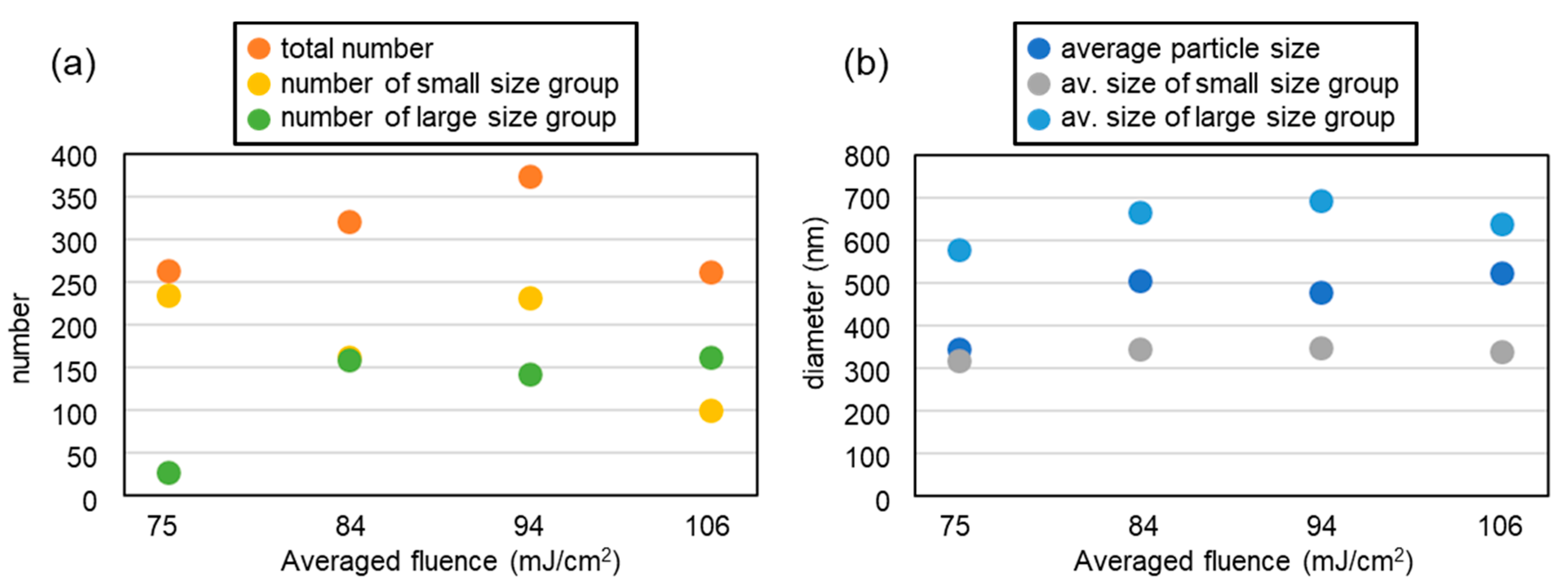
| Averaged Fluence (mJ/cm2) | (a) 106 | (b) 94 | (c) 84 | (d) 75 |
|---|---|---|---|---|
| (a-1) total number | 263 | 375 | 322 | 264 |
| (a-2) number of small size group | 100 | 233 | 162 | 236 |
| (a-3) number of large size group | 163 | 142 | 160 | 28 |
| (b-1) average particle size | 526 | 480 | 506 | 347 |
| (b-2) average size of small size group | 339 | 349 | 345 | 319 |
| (b-3) average size of large size group | 641 | 698 | 668 | 581 |
| (c-1) standard deviation (SD) | 151 | 176 | 171 | 88 |
| (c-2) SD of small size group | 48 | 58 | 62 | 36 |
| (c-3) SD of large size group | 46 | 52 | 50 | 30 |
Publisher’s Note: MDPI stays neutral with regard to jurisdictional claims in published maps and institutional affiliations. |
© 2021 by the authors. Licensee MDPI, Basel, Switzerland. This article is an open access article distributed under the terms and conditions of the Creative Commons Attribution (CC BY) license (http://creativecommons.org/licenses/by/4.0/).
Share and Cite
Nakata, Y.; Tsubakimoto, K.; Miyanaga, N.; Narazaki, A.; Shoji, T.; Tsuboi, Y. Laser-Induced Transfer of Noble Metal Nanodots with Femtosecond Laser-Interference Processing. Nanomaterials 2021, 11, 305. https://doi.org/10.3390/nano11020305
Nakata Y, Tsubakimoto K, Miyanaga N, Narazaki A, Shoji T, Tsuboi Y. Laser-Induced Transfer of Noble Metal Nanodots with Femtosecond Laser-Interference Processing. Nanomaterials. 2021; 11(2):305. https://doi.org/10.3390/nano11020305
Chicago/Turabian StyleNakata, Yoshiki, Koji Tsubakimoto, Noriaki Miyanaga, Aiko Narazaki, Tatsuya Shoji, and Yasuyuki Tsuboi. 2021. "Laser-Induced Transfer of Noble Metal Nanodots with Femtosecond Laser-Interference Processing" Nanomaterials 11, no. 2: 305. https://doi.org/10.3390/nano11020305
APA StyleNakata, Y., Tsubakimoto, K., Miyanaga, N., Narazaki, A., Shoji, T., & Tsuboi, Y. (2021). Laser-Induced Transfer of Noble Metal Nanodots with Femtosecond Laser-Interference Processing. Nanomaterials, 11(2), 305. https://doi.org/10.3390/nano11020305