
Subtractive Low-Temperature Preparation Route for Porous SiO2 Used for the Catalyst-Assisted Growth of ZnO Field Emitters


Abstract
:1. Introduction
2. Materials and Methods
2.1. Preparation Route for Porous SiO2
2.2. Synthesis of Nanowire-like ZnO Field Emitters
2.3. Field Emission Measurements
3. Results
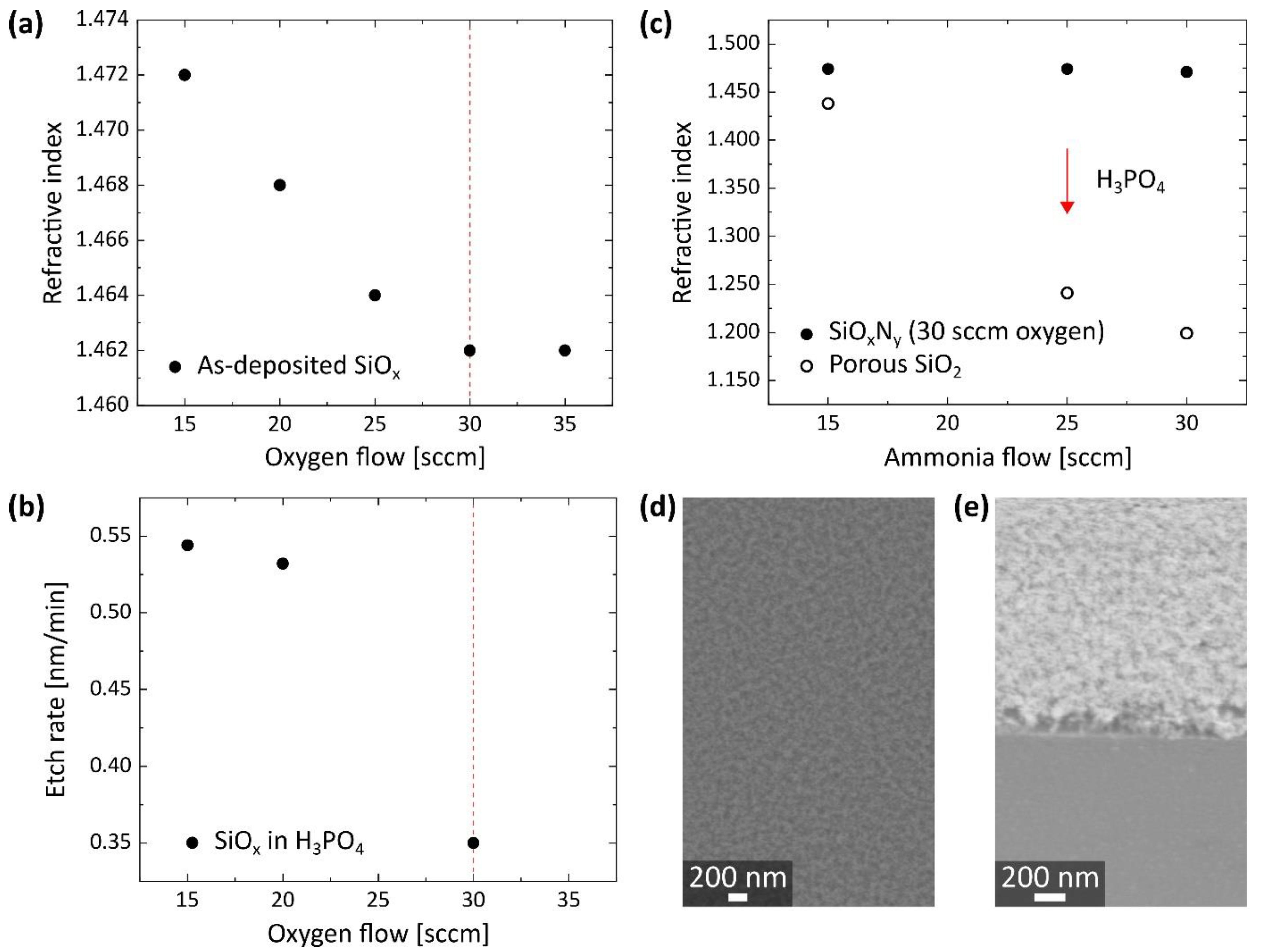
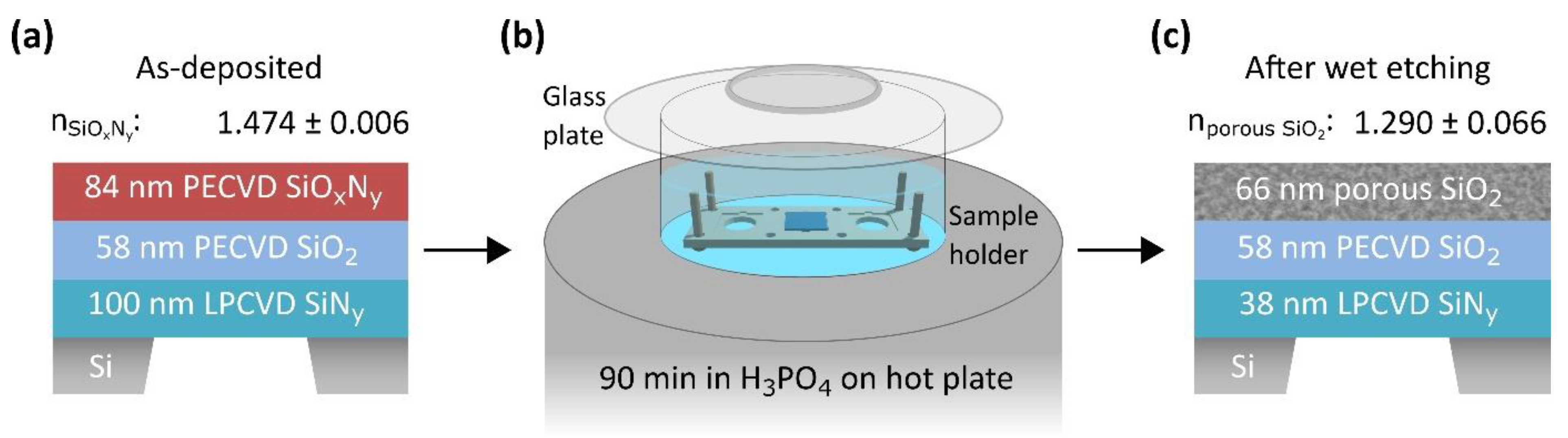
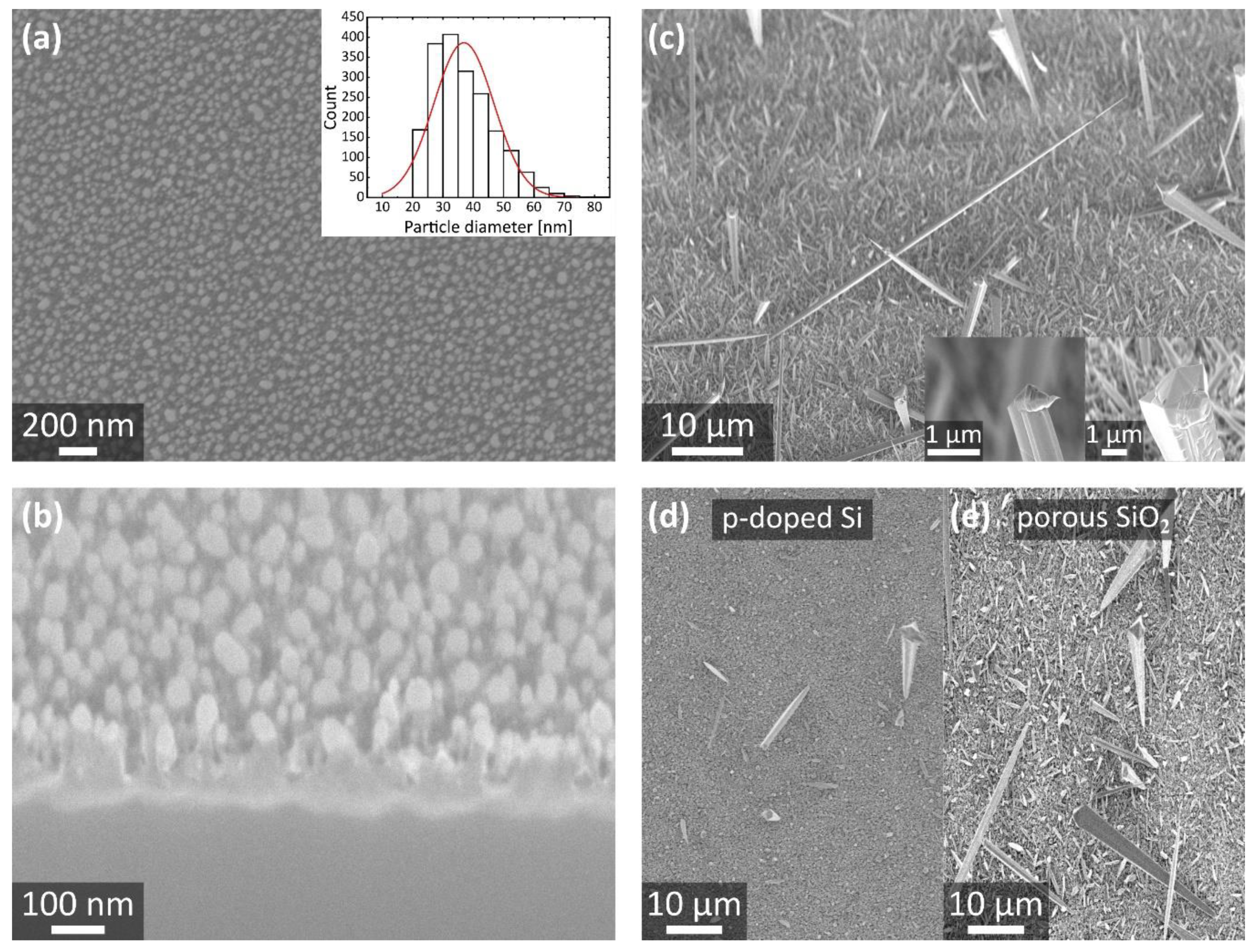
3.1. Synthesis of Porous SiO2 on Bulk Substrates
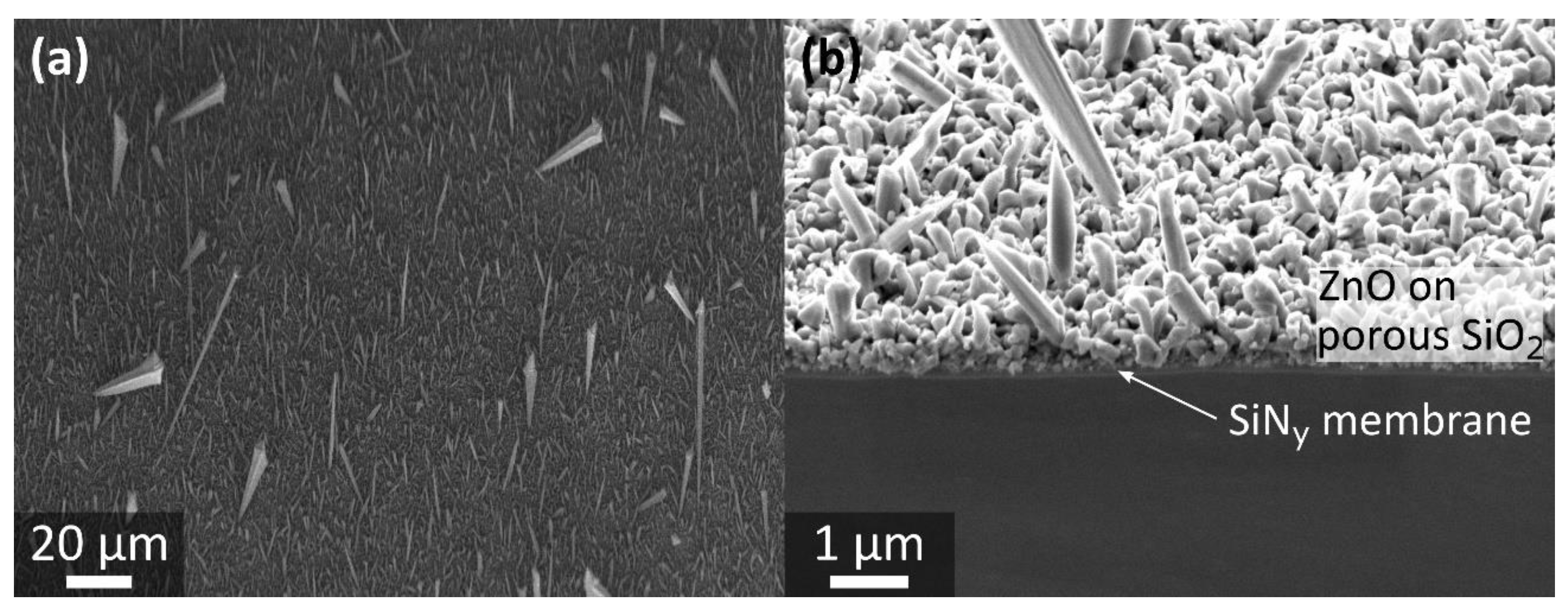
3.2. Synthesis of Porous SiO2 on Free-Standing Membranes
3.3. Porous SiO2 Template—Catalyst-Assisted ZnO Nanowire Growth
3.4. Porous SiO2 Template—Field Emission Measurements
4. Discussion
5. Conclusions
Supplementary Materials
Author Contributions
Funding
Data Availability Statement
Conflicts of Interest
References
- Kim, K.; Kim, S.; An, S.; Lee, G.-H.; Kim, D.; Han, S. Anti-reflection porous SiO2 thin film deposited using reactive high-power impulse magnetron sputtering at high working pressure for use in a-Si:H solar cells. Sol. Energy Mater. Sol. Cells 2014, 130, 582–586. [Google Scholar] [CrossRef]
- Raut, H.K.; Ganesh, V.A.; Nair, A.S.; Ramakrishna, S. Anti-reflective coatings: A critical, in-depth review. Energy Environ. Sci. 2011, 4, 3779–3804. [Google Scholar] [CrossRef]
- Alam, K.; Ali, S.; Saboor, A.; Salman, M.; Maoz; Humayun, M.; Sadiq, M.; Arif, M. Antireflection, superhydrophilic nano-porous SiO2 coating based on aerosol impact spray deposition technique for solar PV module. Coatings 2019, 9, 497. [Google Scholar] [CrossRef] [Green Version]
- Yoldas, B.E. Investigations of porous oxides as an antireflective coating for glass surfaces. Appl. Opt. 1980, 19, 1425–1429. [Google Scholar] [CrossRef] [PubMed]
- Nagel, H.; Aberle, A.G.; Hezel, R. Optimised antireflection coatings for planar silicon solar cells using remote PECVD silicon nitride and porous silicon dioxide. Prog. Photovolt Res. Appl. 1999, 7, 245–260. [Google Scholar] [CrossRef]
- Guo, X.; Quan, X.; Li, Z.; Li, Q.; Zhang, B.; Zhang, X.; Song, C. Broadband anti-reflection coatings fabricated by precise time-controlled and oblique-angle deposition methods. Coatings 2021, 11, 492. [Google Scholar] [CrossRef]
- Raut, H.K.; Nair, A.S.; Dinachali, S.S.; Ganesh, V.A.; Walsh, T.M.; Ramakrishna, S. Porous SiO2 anti-reflective coatings on large-area substrates by electrospinning and their application to solar modules. Sol. Energy Mater. Sol. Cells 2013, 111, 9–15. [Google Scholar] [CrossRef]
- Ghazaryan, L.; Kley, E.-B.; Tünnermann, A.; Szeghalmi, A. Nanoporous SiO2 thin films made by atomic layer deposition and atomic etching. Nanotechnology 2016, 27, 255603. [Google Scholar] [CrossRef]
- Yang, P.-Z.; Liu, L.-M.; Mo, J.-H.; Yang, W. Characterization of PECVD grown porous SiO2 thin films with potential application in an uncooled infrared detector. Semicond. Sci. Technol. 2010, 25, 045017. [Google Scholar] [CrossRef]
- Barranco, A.; Cotrino, J.; Yubero, F.; Espinós, J.P.; González-Elipe, A.R. Room temperature synthesis of porous SiO2 thin films by plasma enhanced chemical vapor deposition. J. Vac. Sci. Technol. A 2004, 22, 1275–1284. [Google Scholar] [CrossRef] [Green Version]
- Nagel, H.; Metz, A.; Hezel, R. Porous SiO2 films prepared by remote plasma-enhanced chemical vapour deposition—A novel antireflection coating technology for photovoltaic modules. Sol. Energy Mater. Sol. Cells 2001, 65, 71–77. [Google Scholar] [CrossRef]
- Thompson, C.V. Solid-state dewetting of thin films. Annu. Rev. Mater. Res. 2012, 42, 399–434. [Google Scholar] [CrossRef]
- Sui, M.; Gong, P.; Gu, X. Review on one-dimensional ZnO nanostructures for electron field emitters. Front. Optoelectron. 2013, 6, 386–412. [Google Scholar] [CrossRef]
- Giubileo, F.; di Bartolomeo, A.; Iemmo, L.; Luongo, G.; Urban, F. Field emission from carbon nanostructures. Appl. Sci. 2018, 8, 526. [Google Scholar] [CrossRef] [Green Version]
- Yi, G.-C.; Wang, C.; Park, W.I. ZnO nanorods: Synthesis, characterization and applications. Semicond. Sci. Technol. 2005, 20, S22–S34. [Google Scholar] [CrossRef]
- Klingshirn, C.F.; Meyer, B.K.; Waag, A.; Hoffmann, A.; Geurts, J. Crystal Structure, Chemical Binding, and Lattice. In Zinc Oxide: From Fundamental Properties Towards Novel Applications, 1st ed.; Springer: Berlin/Heidelberg, Germany, 2010; pp. 8–10. [Google Scholar]
- Nicolaescu, D. Modeling of the field emitter triode (FET) as a displacement/pressure sensor. Appl. Surf. Sci. 1995, 87/88, 61–68. [Google Scholar] [CrossRef]
- Badi, N.; Nair, A.M.; Bensaoula, A. Field emission pressure sensors with non-silicon membranes. Appl. Surf. Sci. 2010, 256, 4990–4994. [Google Scholar] [CrossRef]
- Park, J.; Qin, H.; Scalf, M.; Hilger, R.T.; Westphall, M.S.; Smith, L.M.; Blick, R.H. A mechanical nanomembrane detector for time-of-flight mass spectrometry. Nano Lett. 2011, 11, 3681–3684. [Google Scholar] [CrossRef]
- Hedrich, C.; Haugg, S.; Pacarizi, L.; Furlan, K.P.; Blick, R.H.; Zierold, R. Low-temperature vapor-solid growth of ZnO nanowhiskers for electron field emission. Coatings 2019, 9, 698. [Google Scholar] [CrossRef] [Green Version]
- Schneider, C.A.; Rasband, W.S.; Eliceiri, K.W. NIH Image to ImageJ: 25 years of image analysis. Nat. Methods 2012, 9, 671–675. [Google Scholar] [CrossRef]
- Goldstein, J.I.; Newbury, D.E.; Michael, J.R.; Ritchie, N.W.M.; Scott, J.H.J.; Joy, D.C. Image Formation. In Scanning Electron Microscopy and X-ray Microanalysis, 4th ed.; Springer: New York, NY, USA, 2018; p. 100. [Google Scholar]
- Henkel, C.; Zierold, R.; Kommini, A.; Haugg, S.; Thomason, C.; Aksamija, Z.; Blick, R.H. Resonant tunneling induced enhancement of electron field emission by ultra-thin coatings. Sci. Rep. 2019, 9, 6840. [Google Scholar] [CrossRef]
- Van Gelder, W.; Hauser, V.E. The etching of silicon nitride in phosphoric acid with silicon dioxide as a mask. J. Electrochem. Soc. 1967, 114, 869. [Google Scholar] [CrossRef]
- Jeong, S.-H.; Kim, J.-K.; Kim, B.-S.; Shim, S.-H.; Lee, B.-T. Characterization of SiO2 and TiO2 films prepared using rf magnetron sputtering and their application to anti-reflection coating. Vacuum 2004, 76, 507–515. [Google Scholar] [CrossRef]
- Hiller, D.; Zierold, R.; Bachmann, J.; Alexe, M.; Yang, Y.; Gerlach, J.W.; Stesmans, A.; Jivanescu, M.; Müller, U.; Vogt, J.; et al. Low temperature silicon dioxide by thermal atomic layer deposition: Investigation of material properties. J. Appl. Phys. 2010, 107, 064314. [Google Scholar] [CrossRef] [Green Version]
- Kijaszek, W.; Oleszkiewicz, W.; Zakrzewski, A.; Patela, S.; Tłaczała, M. Investigation of optical properties of silicon oxynitride films deposited by RF PECVD method. Mater. Sci. 2016, 34, 868–871. [Google Scholar] [CrossRef] [Green Version]
- Dwyer, J.R.; Harb, M. Through a window, brightly: A review of selected nanofabricated thin-film platforms for spectroscopy, imaging, and detection. Appl. Spectrosc. 2017, 71, 2051–2075. [Google Scholar] [CrossRef]
- Fan, H.J.; Werner, P.; Zacharias, M. Semiconductor nanowires: From self-organization to patterned growth. Small 2006, 2, 700–717. [Google Scholar] [CrossRef]
- Fulton, A.J.; Kollath, V.O.; Karan, K.; Shi, Y. Gold nanoparticle assembly on porous silicon by pulsed laser induced dewetting. Nanoscale Adv. 2020, 2, 896–905. [Google Scholar] [CrossRef] [Green Version]
- Zhao, X.; Lee, U.-J.; Lee, K.-H. Dewetting behavior of Au films on porous substrates. Thin Solid Films 2010, 519, 706–713. [Google Scholar] [CrossRef]
- Wang, D.; Ji, R.; Schaaf, P. Formation of precise 2D Au particle arrays via thermally induced dewetting on pre-patterned substrates. Beilstein J. Nanotechnol. 2011, 2, 318–326. [Google Scholar] [CrossRef]
- Huang, M.H.; Wu, Y.; Feick, H.; Tran, N.; Weber, E.; Yang, P. Catalytic growth of zinc oxide nanowires by vapor transport. Adv. Mater. 2001, 13, 113–116. [Google Scholar] [CrossRef]
- Forbes, R.G. Extraction of emission parameters for large-area field emitters, using a technically complete Fowler-Nordheim-type equation. Nanotechnology 2012, 23, 095706. [Google Scholar] [CrossRef] [PubMed] [Green Version]
- Matsuda, A.; Matsuno, Y.; Tatsumisago, M.; Minami, T. Changes in porosity and amounts of adsorbed water in sol-gel derived porous silica films with heat treatment. J. Sol-Gel Sci. Technol. 2001, 20, 129–134. [Google Scholar] [CrossRef]
- Yang, S.; Zhang, Y. Spectroscopic ellipsometry investigations of porous SiO2 films prepared by glancing angle deposition. Surf. Interface Anal. 2013, 45, 1690–1694. [Google Scholar] [CrossRef]
- Astrova, E.V.; Tolmachev, V.A. Effective refractive index and composition of oxidized porous silicon films. Mater. Sci. Eng. B Solid-State Mater. Adv. Technol. 2000, 69, 142–148. [Google Scholar] [CrossRef]
- Konjhodzic, D.; Bretinger, H.; Wilczok, U.; Dreier, A.; Ladenburger, A.; Schmidt, M.; Eich, M.; Marlow, F. Low-n mesoporous silica films: Structure and properties. Appl. Phys. A Mater. Sci. Process. 2005, 81, 425–432. [Google Scholar] [CrossRef]
- Xi, J.-Q.; Schubert, M.F.; Kim, J.K.; Schubert, E.F.; Chen, M.; Lin, S.Y.; Liu, W.; Smart, J.A. Optical thin-film materials with low refractive index for broadband elimination of Fresnel reflection. Nat. Photonics 2007, 1, 176–179. [Google Scholar] [CrossRef]
- Borrás, A.; Barranco, A.; González-Elipe, A.R. Design and control of porosity in oxide thin films grown by PECVD. J. Mater. Sci. 2006, 41, 5220–5226. [Google Scholar] [CrossRef]
- Dultsev, F.N.; Solowjev, A.P. Synthesis and ellipsometric characterization of insulating low permittivity SiO2 layers by remote-PECVD using radio-frequency glow discharge. Thin Solid Films 2002, 419, 27–32. [Google Scholar] [CrossRef]
- Boissiere, C.; Grosso, D.; Lepoutre, S.; Nicole, L.; Bruneau, A.B.; Sanchez, C. Porosity and mechanical properties of mesoporous thin films assessed by environmental ellipsometric porosimetry. Langmuir 2005, 21, 12362–12371. [Google Scholar] [CrossRef]
- Fang, X.; Bando, Y.; Gautam, U.K.; Ye, C.; Golberg, D. Inorganic semiconductor nanostructures and their field-emission applications. J. Mater. Chem. 2008, 18, 509–522. [Google Scholar] [CrossRef]
- De Jonge, N.; Bonard, J.-M. Carbon nanotube electron sources and applications. Philos. Trans. R. Soc. Lond. A 2004, 362, 2239–2266. [Google Scholar] [CrossRef] [PubMed]
- Purcell, S.T.; Vincent, P.; Journet, C.; Binh, V.T. Hot nanotubes: Stable heating of individual multiwall carbon nanotubes to 2000 K induced by the field-emission current. Phys. Rev. Lett. 2002, 88, 105502. [Google Scholar] [CrossRef] [PubMed] [Green Version]
- Aroutiounian, V.M.; Martirosyan, K.; Soukiassian, P. Almost zero reflectance of a silicon oxynitride/porous silicon double layer antireflection coating for silicon photovoltaic cells. J. Phys. D Appl. Phys. 2006, 39, 1623–1625. [Google Scholar] [CrossRef]
- Shi, Y.; He, L.; Guang, F.; Li, L.; Xin, Z.; Liu, R. A review: Preparation, performance, and applications of silicon oxynitride film. Micromachines 2019, 10, 552. [Google Scholar] [CrossRef] [PubMed] [Green Version]

Publisher’s Note: MDPI stays neutral with regard to jurisdictional claims in published maps and institutional affiliations. |
© 2021 by the authors. Licensee MDPI, Basel, Switzerland. This article is an open access article distributed under the terms and conditions of the Creative Commons Attribution (CC BY) license (https://creativecommons.org/licenses/by/4.0/).
Share and Cite
Haugg, S.; Hedrich, C.; Blick, R.H.; Zierold, R. Subtractive Low-Temperature Preparation Route for Porous SiO2 Used for the Catalyst-Assisted Growth of ZnO Field Emitters. Nanomaterials 2021, 11, 3357. https://doi.org/10.3390/nano11123357
Haugg S, Hedrich C, Blick RH, Zierold R. Subtractive Low-Temperature Preparation Route for Porous SiO2 Used for the Catalyst-Assisted Growth of ZnO Field Emitters. Nanomaterials. 2021; 11(12):3357. https://doi.org/10.3390/nano11123357
Chicago/Turabian StyleHaugg, Stefanie, Carina Hedrich, Robert H. Blick, and Robert Zierold. 2021. "Subtractive Low-Temperature Preparation Route for Porous SiO2 Used for the Catalyst-Assisted Growth of ZnO Field Emitters" Nanomaterials 11, no. 12: 3357. https://doi.org/10.3390/nano11123357
APA StyleHaugg, S., Hedrich, C., Blick, R. H., & Zierold, R. (2021). Subtractive Low-Temperature Preparation Route for Porous SiO2 Used for the Catalyst-Assisted Growth of ZnO Field Emitters. Nanomaterials, 11(12), 3357. https://doi.org/10.3390/nano11123357