
Traceable Nanoscale Measurements of High Dielectric Constant by Scanning Microwave Microscopy

 , ,
, ,
Abstract
:1. Introduction
2. Materials and Methods
2.1. Experimental Set-Up
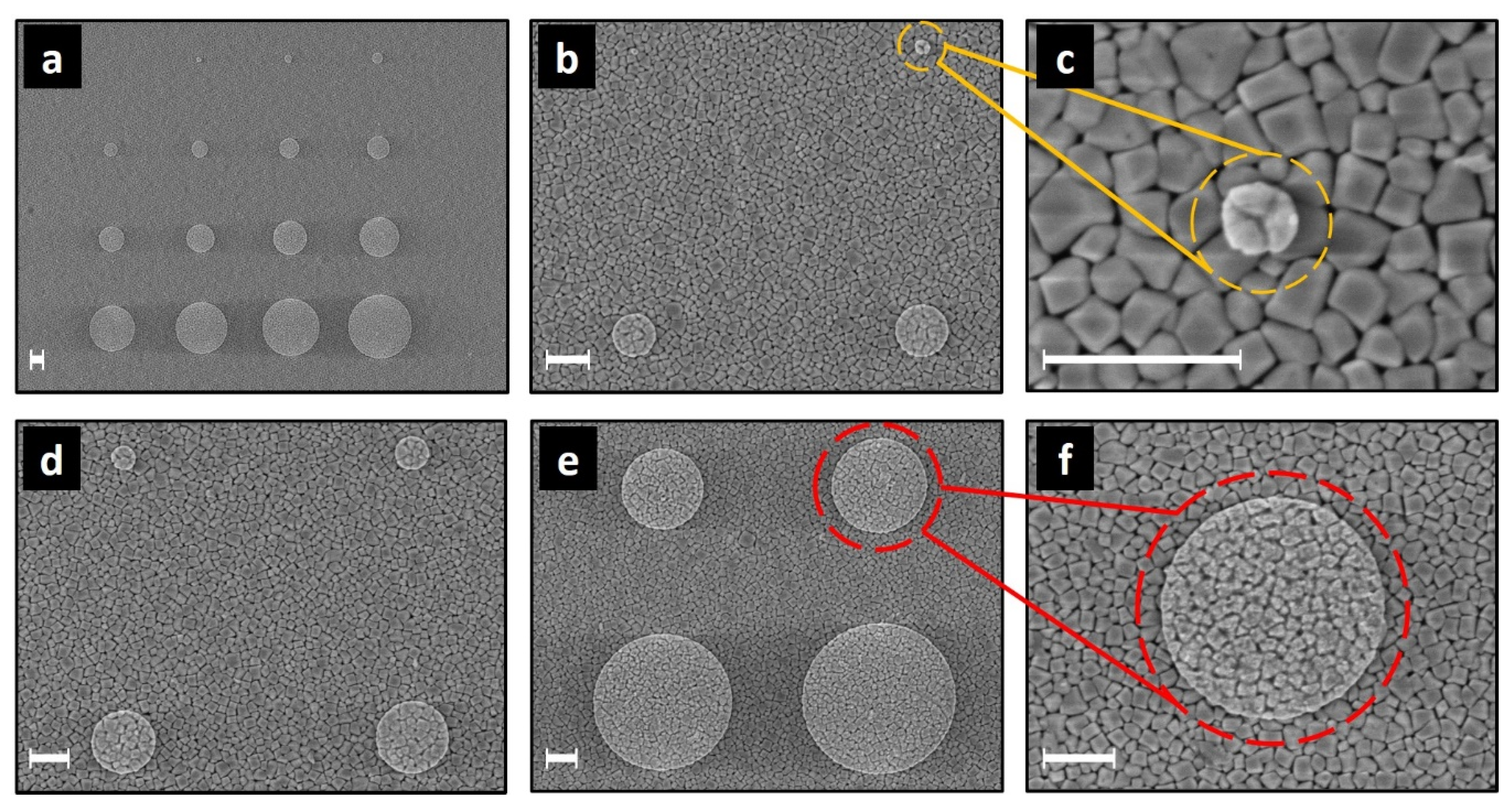
2.2. Samples
2.2.1. Reference Samples
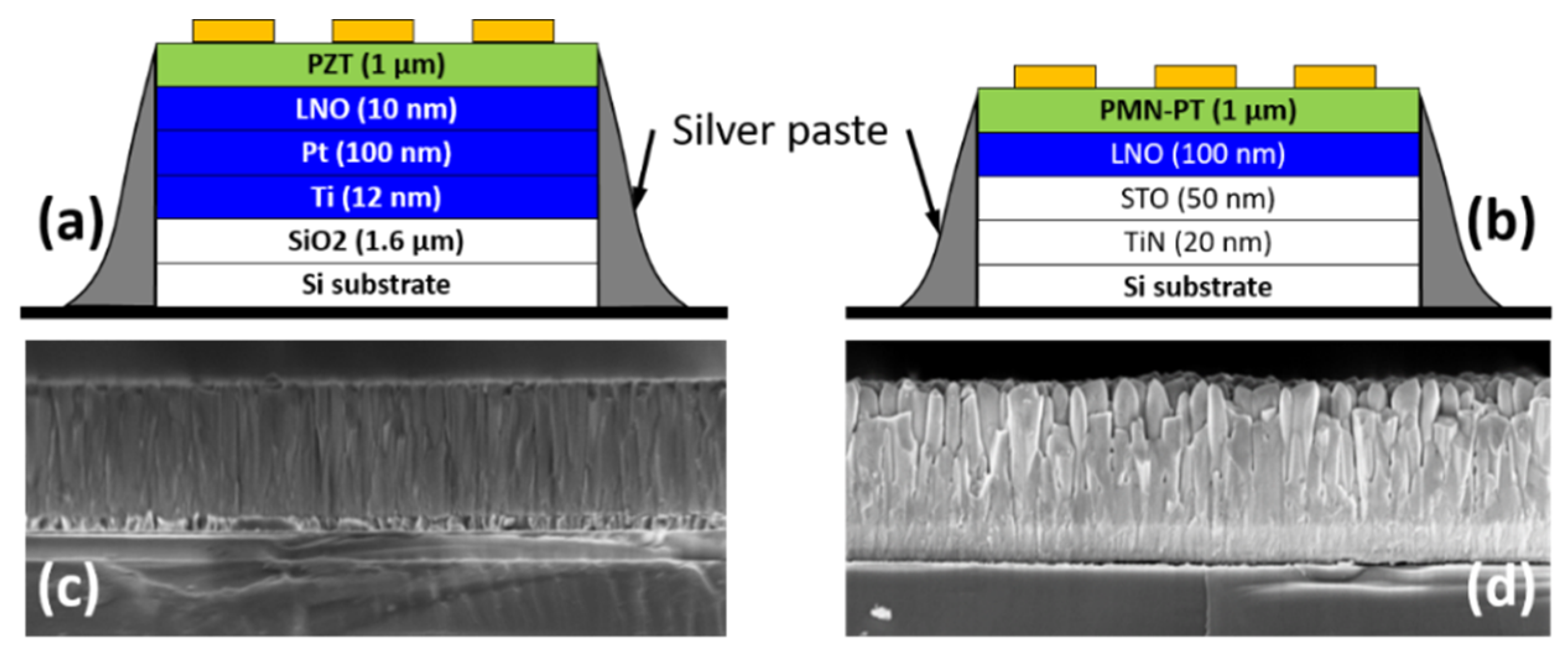
2.2.2. Piezoelectric Samples
2.3. Calibration Method
2.4. Measurement Protocol
3. Results
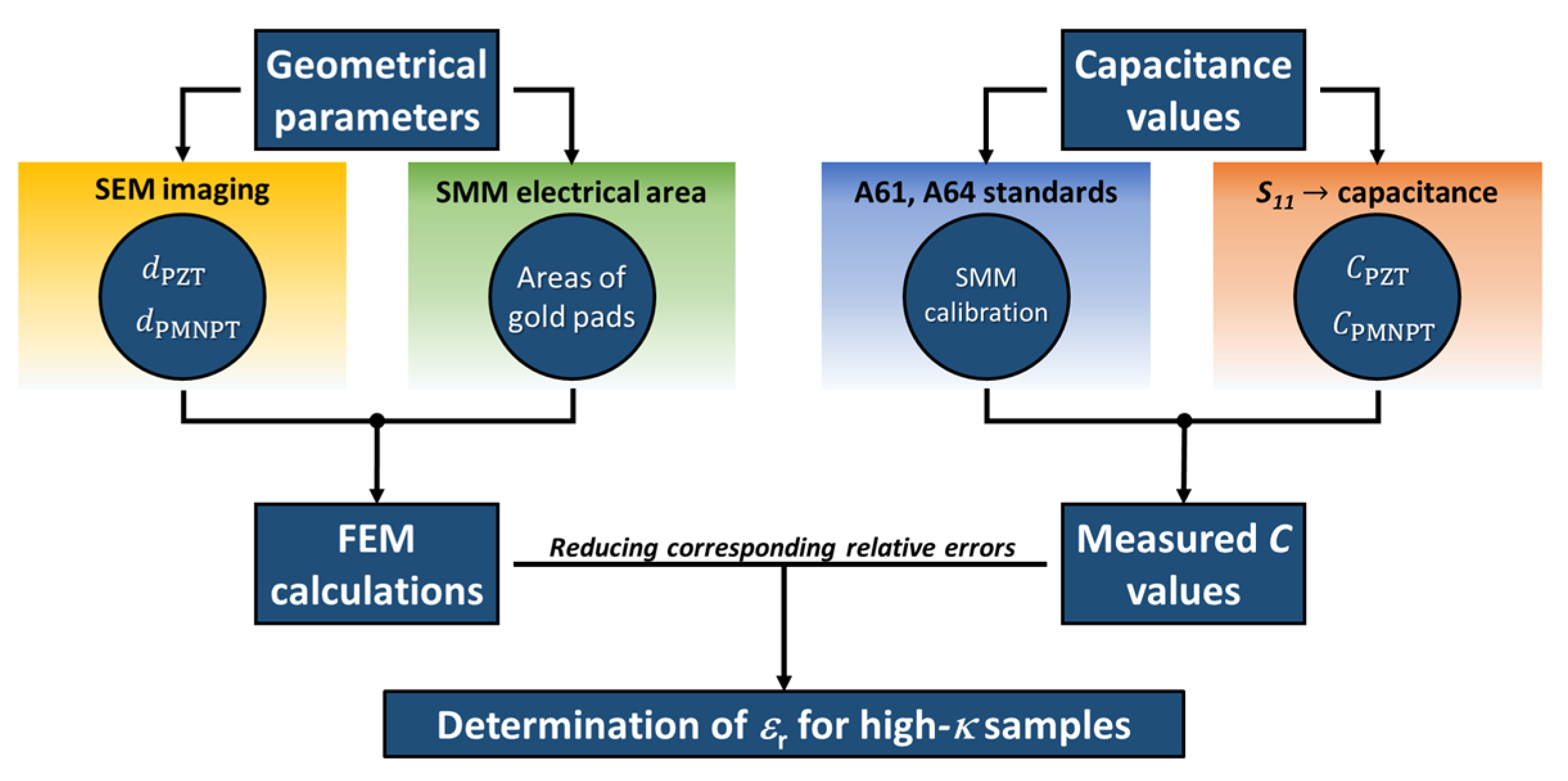
3.1. Capacitance Model
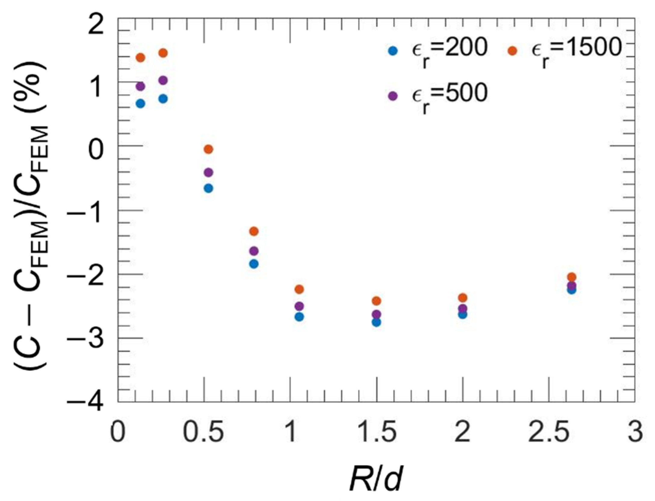
3.1.1. Theory
3.1.2. Dimensional Measurements
- Layer thickness
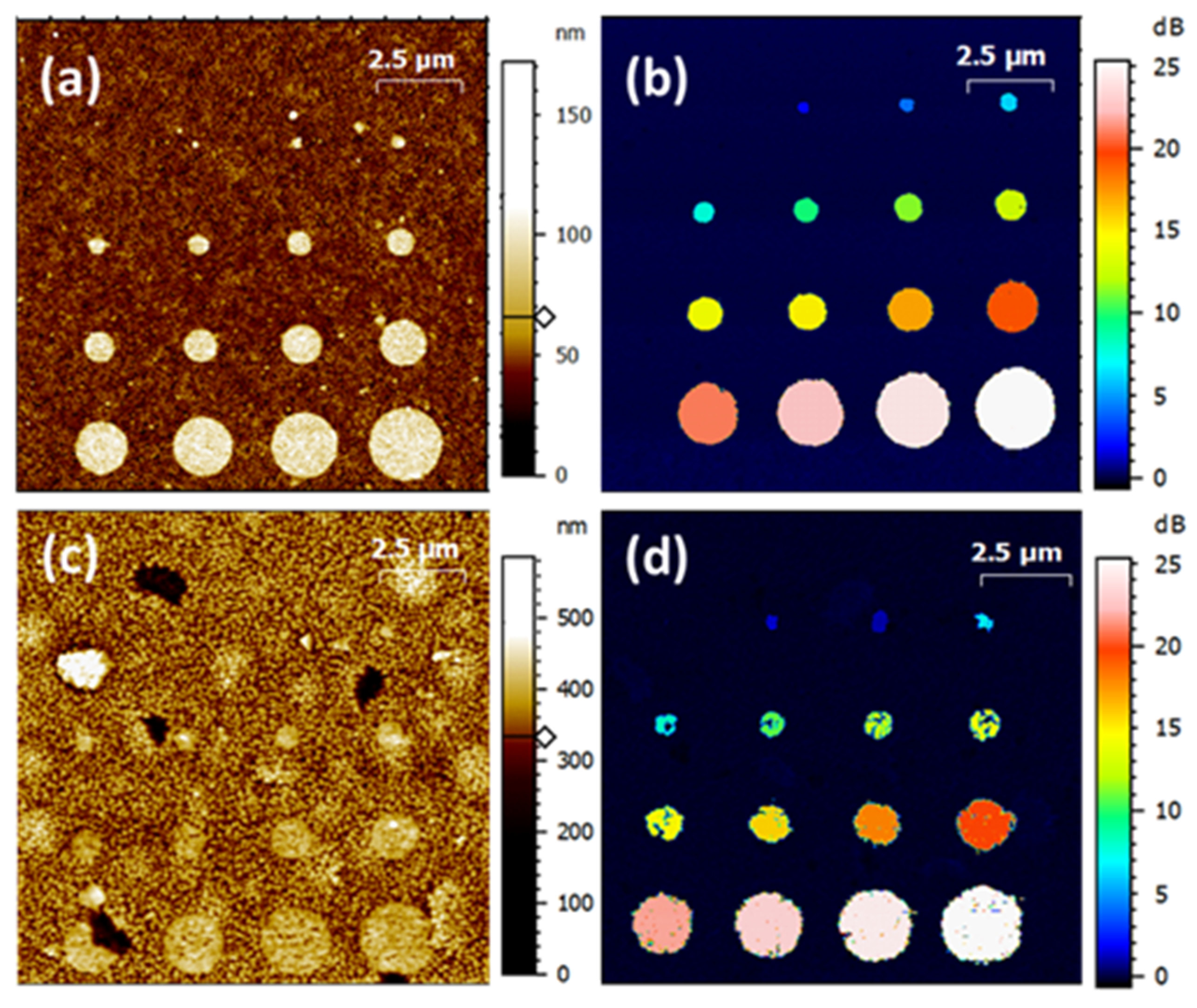
- Gold pad areas
3.2. Capacitance Measurements
3.2.1. Dielectric Constant Determination
3.2.2. Frequency Measurements
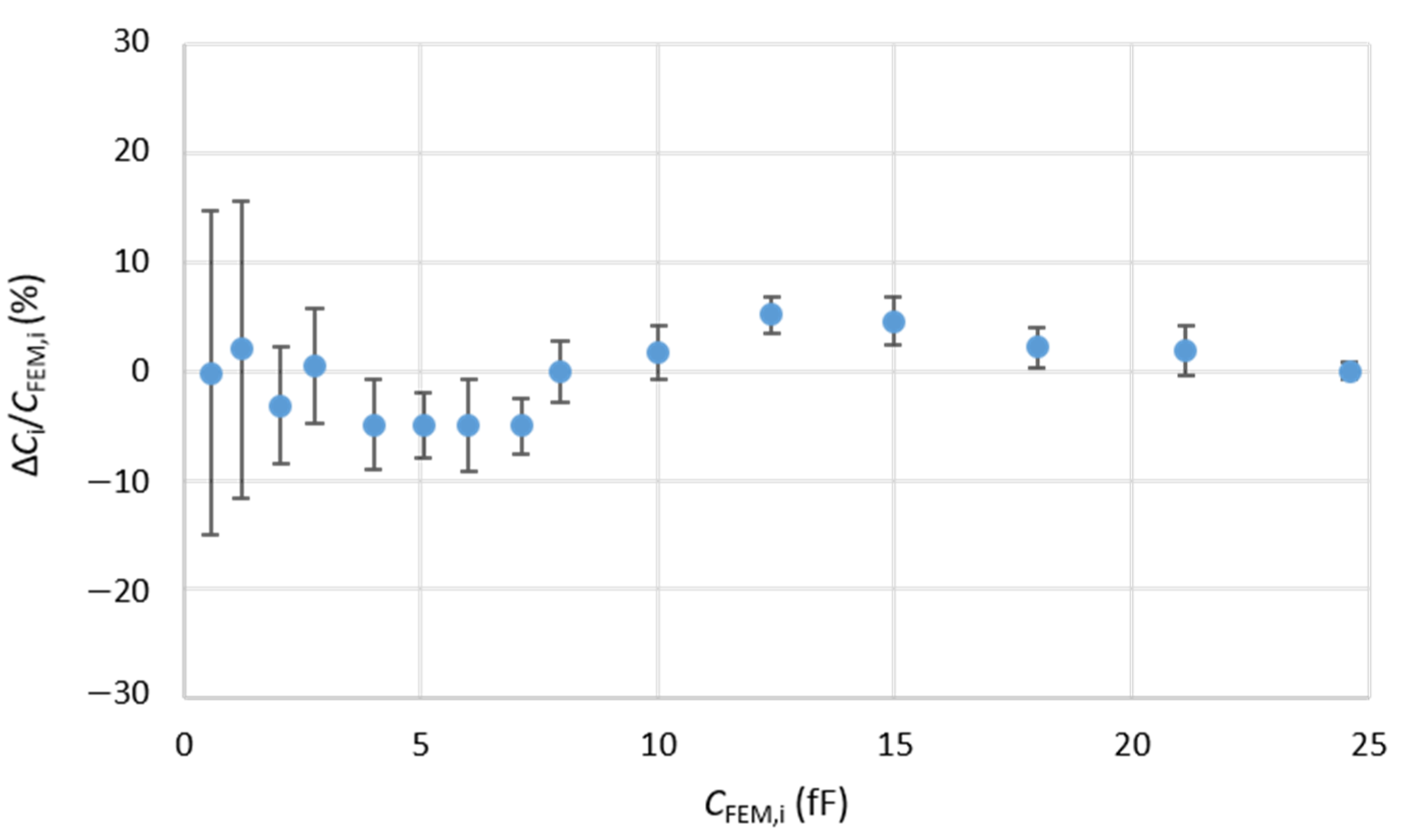
3.3. Uncertainty Budget
4. Discussion
5. Conclusions
Author Contributions
Funding
Institutional Review Board Statement
Informed Consent Statement
Data Availability Statement
Acknowledgments
Conflicts of Interest
References
- Wallace, R.M. Dielectric Materials for Microelectronics. In Springer Handbook of Electronic and Photonic Materials; Kasap, S., Capper, P., Eds.; Springer: Cham, Switzerland, 2017; pp. 615–644. ISBN 9783319489339. [Google Scholar]
- International Technology Roadmap for Semiconductors 2015 Edition “More Moore”; Semiconductor Industry Association: Washington, DC, USA, 2015.
- Sicard, E. Introducing 10-nm FinFET Technology in Microwind. HAL Id hal-01558775 2017. Available online: https://hal.archives-ouvertes.fr/hal-01551695 (accessed on 17 November 2021).
- Bottoms, B. 2019 HIR Chapter 15: Materials and Emerging Research Materials; IEEE Electronics Packaging Society (EPS): 2019. Available online: http://eps.ieee.org/hir (accessed on 17 November 2021).
- Kingon, A.I.; Maria, J.; Streiffer, S.K. Alternative dielectrics to silicon dioxide for memory and logic devices. Nature 2000, 406, 1032–1038. [Google Scholar] [CrossRef]
- Robertson, J. High dielectric constant oxides. Eur. Phys. J.-Appl. Phys. 2004, 28, 265–291. [Google Scholar] [CrossRef] [Green Version]
- Yim, K.; Yong, Y.; Lee, J.; Lee, K.; Nahm, H.H.; Yoo, J.; Lee, C.; Hwang, C.S.; Han, S. Novel high-Κ dielectrics for next-generation electronic devices screened by automated ab initio calculations. NPG Asia Mater. 2015, 7, e190. [Google Scholar] [CrossRef]
- Benech, P.; Duchamp, J.-M. Piezoelectric Materials in RF Applications. In Piezoelectric Materials; Ogawa, T., Ed.; IntechOpen: London, UK, 2016. [Google Scholar]
- Chang, S.W.; Oh, J.; Boles, S.T.; Thompson, C.V. Fabrication of silicon nanopillar-based nanocapacitor arrays. Appl. Phys. Lett. 2010, 96, 153108. [Google Scholar] [CrossRef]
- Son, J.Y.; Shin, Y.H.; Kim, H.; Jang, H.M. NiO resistive random access memory nanocapacitor array on graphene. ACS Nano 2010, 4, 2655–2658. [Google Scholar] [CrossRef] [PubMed]
- Li, L.J.; Zhu, B.; Ding, S.J.; Lu, H.L.; Sun, Q.Q.; Jiang, A.; Zhang, D.W.; Zhu, C. Three-dimensional AlZnO/Al2O3/AlZnO nanocapacitor arrays on Si substrate for energy storage. Nanoscale Res. Lett. 2012, 7, 544. [Google Scholar] [CrossRef] [Green Version]
- Wei, L.; Liu, Q.; Zhu, B.; Liu, W.; Ding, S.; Lu, H.; Jiang, A.; Zhang, D.W. Low-Cost and High-Productivity Three- Dimensional Nanocapacitors Based on Stand-Up ZnO Nanowires for Energy Storage. Nanoscale Res. Lett. 2016, 11, 213. [Google Scholar] [CrossRef] [PubMed] [Green Version]
- Ivanova, N.; Gugleva, V.; Dobreva, M.; Pehlivanov, I.; Stefanov, S.; Andonova, V. Piezoelectric Materials in RF Applications. Intech 2016, i, 13. [Google Scholar]
- Tadigadapa, S.; Mateti, K. Piezoelectric MEMS sensors: State-of-the-art and perspectives. Meas. Sci. Technol. 2009, 20, 092001. [Google Scholar] [CrossRef]
- Larson, J.D.; Gilbert, S.R.; Xu, B. PZT Material properties at UHF and microwave frequencies derived from FBAR measurements. In Proceedings of the IEEE Ultrasonics Symposium, Montreal, QC, Canada, 23–27 August 2004; IEEE: Piscataway, NJ, USA, 2004; Volume 1, pp. 173–177. [Google Scholar]
- Tierno, D.; Dekkers, M.; Wittendorp, P.; Sun, X.; Bayer, S.C.; King, S.T.; Van Elshocht, S.; Heyns, M.; Radu, I.P.; Adelmann, C. Microwave Characterization of Ba-substituted PZT and ZnO Thin Films. IEEE Trans. Ultrason. Ferroelectr. Freq. Control 2018, 65, 881–888. [Google Scholar] [CrossRef]
- Vogel, E.M. Technology and metrology of new electronic materials and devices. Nat. Nanotechnol. 2007, 2, 25–32. [Google Scholar] [CrossRef]
- Aftabjahani, S.; Ameen, A.; Robert, B.; Jeff, B.; Rosario, C. Semiconductor Research Opportunities: An Industry Vision and Guide; Semiconductor Industry Association: Washington, DC, USA, 2017. [Google Scholar]
- Tselev, A.; Yu, P.; Cao, Y.; Dedon, L.R.; Martin, L.W.; Kalinin, S.V.; Maksymovych, P. Microwave a.c. conductivity of domain walls in ferroelectric thin film. Nat. Commun. 2016, 7, 11630. [Google Scholar] [CrossRef] [PubMed] [Green Version]
- Karbassi, A.; Ruf, D.; Bettermann, A.D.; Paulson, C.A.; Weide, D.W. Van Der Quantitative scanning near-field microwave microscopy for thin film dielectric constant measurement Quantitative scanning near-field microwave microscopy for thin film dielectric constant measurement. Rev. Sci. Instrum. 2008, 76, 094706. [Google Scholar] [CrossRef] [PubMed]
- Huber, H.P.; Moertelmaier, M.; Wallis, T.M.; Chiang, C.J.; Hochleitner, M.; Imtiaz, A.; Oh, Y.J.; Schilcher, K.; Dieudonne, M.; Smoliner, J.; et al. Calibrated nanoscale capacitance measurements using a scanning microwave microscope. Rev. Sci. Instrum. 2010, 81, 113701. [Google Scholar] [CrossRef]
- Hoffmann, J.; Gramse, G.; Niegemann, J.; Zeier, M.; Kienberger, F.; Hoffmann, J.; Gramse, G.; Niegemann, J.; Zeier, M. Measuring low loss dielectric substrates with scanning probe microscopes Measuring low loss dielectric substrates with scanning probe microscopes. Appl. Phys. Lett. 2014, 105, 013102. [Google Scholar] [CrossRef]
- Gramse, G.; Kasper, M.; Fumagali, L.; Hinterdorfer, P.; Kienberger, F. Calibrated complex impedance and permittivity measurements with scanning microwave microscopy. Nanotechnology 2014, 25, 145703, Erratum in 2015, 26, 149501. [Google Scholar] [CrossRef]
- Yu, S.; Li, L.; Zhang, W.; Sun, Z.; Dong, H. Multilayer thin films with compsitional PbZrTiO3/BiZnNbO7 layers for tuneable applications. Sci. Rep. 2015, 148, 148–162. [Google Scholar]
- Gagarin, A.; Platonov, R.; Legkova, T.; Altynnikov, A. Estimation of ferroelectric material properties and phase-shifter design key parameters influence on its figure of merit for optimization of development process. Crystals 2021, 11, 538. [Google Scholar] [CrossRef]
- Polcawich, R.G.; Pulskamp, J.S.; Judy, D.; Ranade, P.; Trolier-McKinstry, S.; Dubey, M. Surface Micromachined Microelectromechancial Ohmic Series Switch Using Thin-Film Piezoelectric Actuators. IEEE Trans. Microw. Theory Tech. 2007, 55, 2642–2654. [Google Scholar] [CrossRef]
- Zhai, J.; Xing, Z.; Dong, S.; Li, J.; Viehland, D. Detection of pico-Tesla magnetic fields using magneto-electric sensors at room temperature. Appl. Phys. Lett. 2006, 88, 9–12. [Google Scholar] [CrossRef] [Green Version]
- Zhou, Z.; Zhao, S.; Gao, Y.; Wang, X.; Nan, T.; Sun, N.X.; Yang, X.; Liu, M. The memory effect of magnetoelectric coupling in FeGaB/NiTi/PMN-PT multiferroic heterostructure. Sci. Rep. 2016, 6, 20450. [Google Scholar] [CrossRef] [PubMed] [Green Version]
- Morán-meza, J.A.; Delvallée, A.; Allal, D.; Piquemal, F. A substitution method for nanoscale capacitance calibration using scanning microwave microscopy. Meas. Sci. Technol. 2020, 31, 074009. [Google Scholar] [CrossRef]
- Delvallée, A.; Feltin, N.; Ducourtieux, S.; Trabelsi, M.; Hochepied, J.F. Toward an uncertainty budget for measuring nanoparticles by AFM. Metrologia 2016, 53, 41–50. [Google Scholar] [CrossRef]
- Crouzier, L.; Delvallée, A.; Allard, A.; Devoille, L.; Ducourtieux, S.; Feltin, N. Methodology to evaluate the uncertainty associated with nanoparticle dimensional measurements by SEM. Meas. Sci. Technol. 2019, 30, 085004. [Google Scholar] [CrossRef]
- Piquemal, F.; Morán-meza, J.; Delvallée, A.; Richert, D.; Kaja, K. Progress in traceable nanoscale capacitance measurements using scanning microwave microscopy. Nanomaterials 2021, 11, 820. [Google Scholar] [CrossRef]
- Hoffmann, J.; Wollensack, M.; Zeier, M.; Niegemann, J.; Huber, H. A Calibration Algorithm for Nearfield Scanning Microwave Microscopes. In Proceedings of the 2012 12th IEEE International Conference on Nanotechnology (IEEE-NANO), Birmingham, UK, 20–23 August 2012; pp. 1–4. [Google Scholar]
- Gokul Raj, R.; Krishnamurthy, C.V. Static dielectric constant assessment from capacitance over a wide range of electrode separations. J. Electrost. 2017, 87, 19–25. [Google Scholar] [CrossRef]
- Carlson, G.T.; Illman, B.L. The circular disk parallel plate capacitor. Am. J. Phys. 1994, 62, 1099–1105. [Google Scholar] [CrossRef]
- Paffuti, G.; Cataldo, E.; Di Lieto, A.; Maccarrone, F. Circular plate capacitor with different discs. Proc. R. Soc. Math. Phys. Eng. Sci. 2016, 472, 20160574. [Google Scholar] [CrossRef]
- Patel, Y.; Janusas, G.; Palevicius, A.; Vilkauskas, A.; Lepsik, P. Investigation of the hydrophobic properties of piezoelectric nanocomposites and applications in biomedical micro-hydraulic devices. Mater. Technol. 2020, 54, 407–415. [Google Scholar] [CrossRef]
- Mao, H.; Qiu, M.; Bu, J.; Chen, X.; Verweij, H.; Fan, Y. Self-Cleaning Piezoelectric Membrane for Oil-in-Water Separation. ACS Appl. Mater. Interfaces 2018, 10, 18093–18103. [Google Scholar] [CrossRef]
- Yardin, C. REGPOLY: A software to estimate the calibration function and to compute experimental result. In Proceedings of the International Congress of Metrology, Paris, France, 7–10 October 2013; Volume 04009. [Google Scholar]
- Fischer, R.A. The Conditions under Which χ2 Measures the Discrepancey between Observation and Hypothesis. J. R. Stat. Soc. 1924, 87, 442–450. [Google Scholar]
- Birge, R.T. The calculation of errors by the method of least squares. Phys. Rev. 1932, 40, 207. [Google Scholar] [CrossRef]
- Mohr, P.J.; Taylor, B.N. Codata recommended values of the fundamental physical constants: 2002. Rev. Mod. Phys. 2005, 77, 1. [Google Scholar] [CrossRef] [Green Version]
- JCGM. Evaluation of measurement data—Guide to the expression of uncertainty in measurement. JCGM 2008, 100, 1–116. [Google Scholar]
- Kalpat, S.; Du, X.; Abothu, I.R.; Akiba, A.; Goto, H.; Uchino, K. Effect of Crystal Orientation on Dielectric Properties of Lead Zirconium Titanate Thin Films Prepared by Reactive RF-Sputtering Effect of Crystal Orientation on Dielectric Properties of Lead Zirconium Titanate Thin Films Prepared by Reactive RF-Sputtering. Jpn. J. Appl. Phys. 2001, 40, 713–717. [Google Scholar] [CrossRef]
- Fumagalli, L.; Esfandiar, A.; Fabregas, R.; Hu, S.; Ares, P.; Janardanan, A.; Yang, Q.; Radha, B.; Taniguchi, T.; Watanabe, K.; et al. Anomalously low dielectric constant of confined water. Science 2018, 360, 1339–1342. [Google Scholar] [CrossRef] [Green Version]
- Zhao, Y.-P.; Wang, G.-C.; Lu, T.-M.; Palasantzas, G.; De Hosson, J.T.M. Surface-roughness effect on capacitance and leakage current of an insulating film. Phys. Rev. B 1999, 60, 9157–9164. [Google Scholar] [CrossRef] [Green Version]
- Jin, L. Broadband Dielectric Response in Hard and Soft PZT: Understanding Softening and Hardening Mechanisms. Infoscience 2011, 4988. [Google Scholar] [CrossRef]
- Awang, Z.; Sulaiman, S. PZT and PNZT-based Thin Film Capacitors and Transmission Lines for Microwave Integrated Circuit Applications. In Proceedings of the Second International Conference on Telecommunications and Remote Sensing (ICTRS 2013), Noordwijkerhout, The Netherlands, 11–12 July 2013; pp. 95–103. [Google Scholar]
- Ionescu, D.; Cehan, V. High Frequency Permittivity Determinations for the (PMN–PT)/BaTiO3 Polymer–Ceramic Nanocomposites. In Proceedings of the 33rd International Spring Seminar on Electronics Technology, Warsaw, Poland, 12–16 May 2010; IEEE: Piscataway, NJ, USA, 2010; pp. 332–337. [Google Scholar]
- Fumagalli, L.; Ferrari, G.; Sampietro, M.; Casuso, I.; Mart, E. Nanoscale capacitance imaging with attofarad resolution using ac current sensing atomic force microscopy. Nanotechnology 2006, 17, 4581. [Google Scholar] [CrossRef]
- Fumagalli, L.; Ferrari, G.; Sampietro, M. Dielectric-constant measurement of thin insulating films at low frequency by nanoscale capacitance microscopy. Appl. Phys. Lett. 2007, 91, 243110. [Google Scholar] [CrossRef]
- Gomila, G.; Gramse, G.; Fumagalli, L. Finite-size effects and analytical modeling of electrostatic force microscopy applied to dielectric fi lms. Nanotechnology 2014, 25, 255702. [Google Scholar] [CrossRef] [PubMed]


| Pad Number | Atopo (PZT) (µm2) | uAtopo (PZT) (%) | N |
|---|---|---|---|
| 1 | 0.02 | 7.8 | 4.47 |
| 2 | 0.05 | 9.5 | 2.48 |
| 3 | 0.10 | 3.1 | 2.22 |
| 4 | 0.16 | 3.3 | 1.99 |
| 5 | 0.24 | 2.6 | 1.70 |
| 6 | 0.35 | 1.5 | 1.56 |
| 7 | 0.45 | 1.3 | 1.47 |
| 8 | 0.56 | 1.3 | 1.47 |
| 9 | 0.70 | 1.7 | 1.47 |
| 10 | 1.02 | 1.3 | 1.34 |
| 11 | 1.40 | 1.1 | 1.29 |
| 12 | 1.83 | 1.2 | 1.32 |
| 13 | 2.34 | 1.0 | 1.28 |
| 14 | 2.92 | 1.4 | 1.24 |
| 15 | 3.56 | 0.5 | 1.21 |
| Uncertainty Sources | PZT u (%) | PMN-PT (1st Series) u (%) | PMN-PT (2nd Series) u (%) |
|---|---|---|---|
| Capacitance calculation | (2.5; 9.7) | (6.5; 20.5) | (6.5; 23.6) |
| Area, uA | (1.3; 9.5) | (3.5; 19.7) | (3.4; 22.9) |
| Thickness, ud | 2.1 | 5.5 | 5.5 |
| Capacitance measurements | 3.2 | 3.3 | 3.2 |
| Type-A (Histogram, repeatability) | (0.1; 0.2) | (0.2; 0.6) | (0.2; 0.6) |
| SMM calibration | 3.1 | 3.1 | 3.1 |
| Others | <1.8 | <1.8 | <1.8 |
| Combined uncertainty, uc (%) | 3.5 | 9.1 | 10.6 |
Publisher’s Note: MDPI stays neutral with regard to jurisdictional claims in published maps and institutional affiliations. |
© 2021 by the authors. Licensee MDPI, Basel, Switzerland. This article is an open access article distributed under the terms and conditions of the Creative Commons Attribution (CC BY) license (https://creativecommons.org/licenses/by/4.0/).
Share and Cite
Richert, D.; Morán-Meza, J.; Kaja, K.; Delvallée, A.; Allal, D.; Gautier, B.; Piquemal, F. Traceable Nanoscale Measurements of High Dielectric Constant by Scanning Microwave Microscopy. Nanomaterials 2021, 11, 3104. https://doi.org/10.3390/nano11113104
Richert D, Morán-Meza J, Kaja K, Delvallée A, Allal D, Gautier B, Piquemal F. Traceable Nanoscale Measurements of High Dielectric Constant by Scanning Microwave Microscopy. Nanomaterials. 2021; 11(11):3104. https://doi.org/10.3390/nano11113104
Chicago/Turabian StyleRichert, Damien, José Morán-Meza, Khaled Kaja, Alexandra Delvallée, Djamel Allal, Brice Gautier, and François Piquemal. 2021. "Traceable Nanoscale Measurements of High Dielectric Constant by Scanning Microwave Microscopy" Nanomaterials 11, no. 11: 3104. https://doi.org/10.3390/nano11113104
APA StyleRichert, D., Morán-Meza, J., Kaja, K., Delvallée, A., Allal, D., Gautier, B., & Piquemal, F. (2021). Traceable Nanoscale Measurements of High Dielectric Constant by Scanning Microwave Microscopy. Nanomaterials, 11(11), 3104. https://doi.org/10.3390/nano11113104