Article

Development of a Reflective 193-nm DUV Microscope System for Defect Inspection of Large Optical Surfaces

Center for Scientific Instrumentation, Korea Basic Science Institute, 169-148 Gwahak-ro, Yuseong-gu, Daejeon 34133, Korea
*
Authors to whom correspondence should be addressed.
Appl. Sci. 2019, 9(23), 5205; https://doi.org/10.3390/app9235205
Submission received: 31 October 2019 / Revised: 26 November 2019 / Accepted: 28 November 2019 / Published: 29 November 2019
(This article belongs to the Special Issue Selected Papers from the ICMR 2019)

Abstract

:
We developed a 193-nm deep ultraviolet (DUV) microscope system based on the reflection mode for a precise inspection of various types of defects/cracks on large optical surfaces of the order of one meter in size. Without preprocessing the sample at room temperature and atmospheric pressure, which is commonly necessary for electron microscopy, the reflective 193-nm DUV microscope was used to directly observe optical surface defects in a manner similar to conventional optical microscopes. In addition, the limitations on the selection of materials and thickness of optical samples of transmittive DUV microscopes were overcome. DUV microscope imaging and the analysis on the spatial resolution were verified using a 1D grating structure with a 225-nm line width. This system could be widely applied as an inspection tool because it provides high resolution at the 200-nm scale that is close to the diffraction limit of a 193-nm DUV beam. In the near future, it is expected that our system would be extended to nano/bio imaging as well as the inspection of large optical surfaces.

1. Introduction

Various optical surface metrologies have been studied for the surface inspection of optical elements [1]. There are many criteria used to classify optical surface metrologies; here, we divide them into two kinds of metrologies. One is the macroscopic observation of the overall optical surface (surface figure) of the optical elements, and the other is the microscopic observation of the localized optical surface (surface roughness). Typically, various types of interferometers, such as the Fizeau interferometer [2] and the Twyman–Green interferometer [3], are used for the observation of surface figures. Moreover, for the observation of surface roughness, commercially available metrologies, such as white-light interferometry [4] and scanning probe profilometers [5], are applied. Recently, the size of optical elements extensively applied in space/astronomy [6], X-ray free electron lasers [7], and high-power lasers [8] has increased to the one-meter scale. However, the existing inspection systems for two cases (macroscopic and microscopic) are unable to cope with the optics size, thereby becoming a bottleneck for the development of large optical elements. Currently, the inspection systems for macroscopic observation, such as surface figure, cover optical sizes of the order of a few hundred mm; however, the spatial resolution does not reach the sub-µm range [9,10,11,12]. In inspection systems for microscopic observation, such as surface roughness, the spatial resolution reaches the few hundred nm range, but they are limited to optical sizes of the order of a few tens of mm. Thus, the development of surface inspection systems that can observe large optical surfaces of the order of the one meter-scale together with a spatial resolution of a few hundred nm is necessary.
The enhancement of spatial resolution is one of the most crucial issues for the development of optical microscopes. Currently, state-of-the-art technologies, such as photoactivated localization microscopy (PALM) [13], stimulated emission depletion microscopy (STED) [14], 4pi microscopy [15], confocal microscopy [16], and nonlinear microscopy [17], are being actively developed, and in the modern day, we tend to take nm-level resolution for granted. An alternative to improve the spatial resolution is the use of shorter wavelengths to reduce the diffraction limit of light. Ultraviolet (UV) wavelengths can be applied without a vacuum environment because of the relatively low absorption of UV light at atmospheric pressure, unlike the vacuum conditions required for the use of soft X-rays with a wavelength of a few tens of nm. However, the optical elements available for use at both UV and soft X-ray wavelengths are very limited, contrary to those for visible and infrared wavelengths. In addition, there are limitations on the selection of materials and imaging sample thickness, because recently developed UV microscopes are mainly based on the transmission mode [18,19,20]. The spatial resolution of deep ultraviolet (DUV) microscopes cannot reach the extremely high spatial resolution (~nm scale) of a scanning electron microscope (SEM). Also, DUV microscopes may not be appropriate for the inspection of some UV-sensitive optical materials.
In this paper, a 193-nm DUV microscope system based on the reflection mode was developed coupled with a long traveling translational stage capable of observing large optical surfaces of the one-meter scale. Using a 193-nm ArF laser, the DUV microscope imaging was directly performed without requiring preprocessing of the sample at room temperature and atmospheric pressure. In addition, implementing the reflective DUV microscope removed the limitations on the selection of materials and optical sample thickness. As a result, reflective DUV microscope imaging was demonstrated with a spatial resolution close to the wavelength diffraction limit.

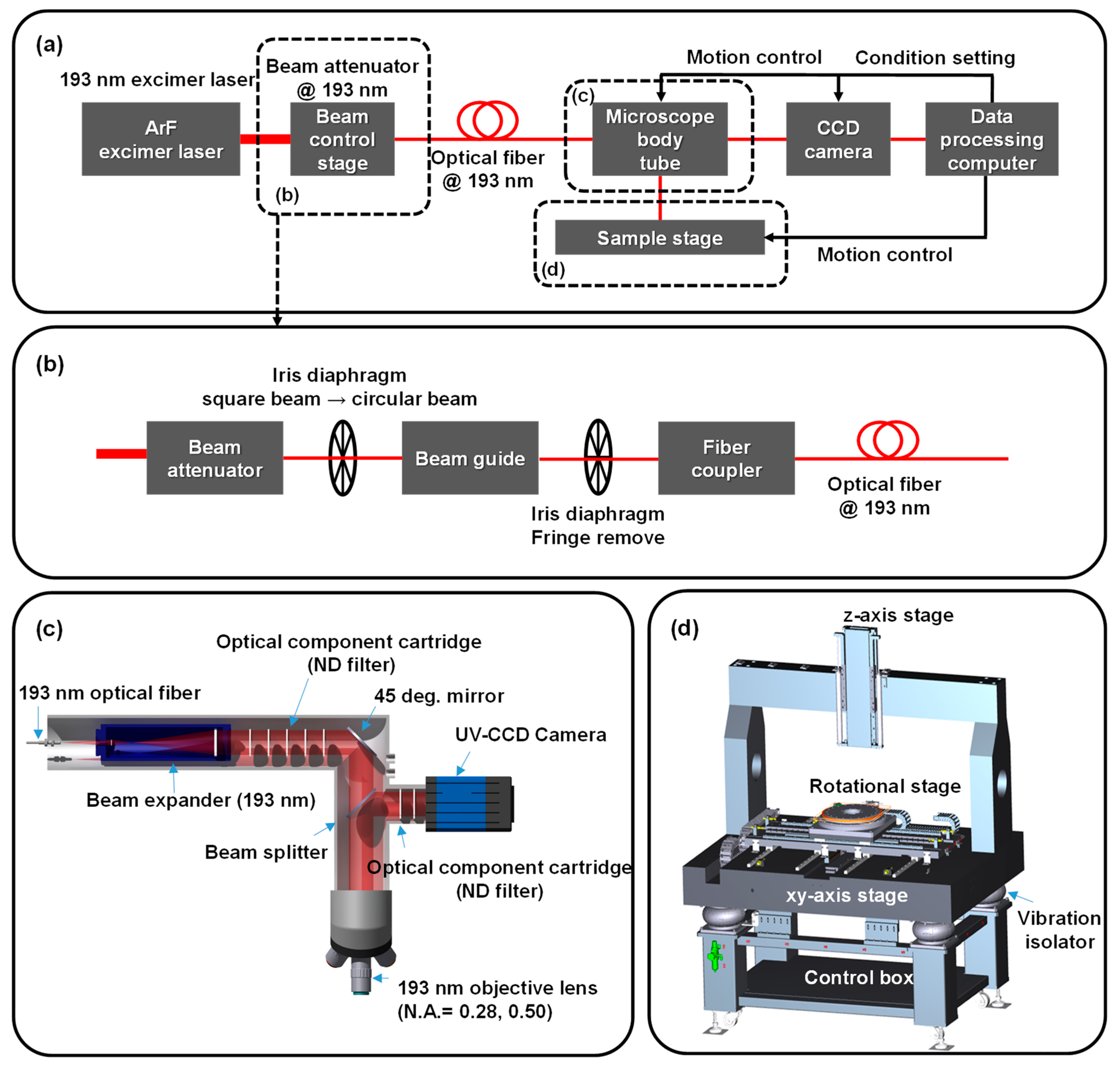
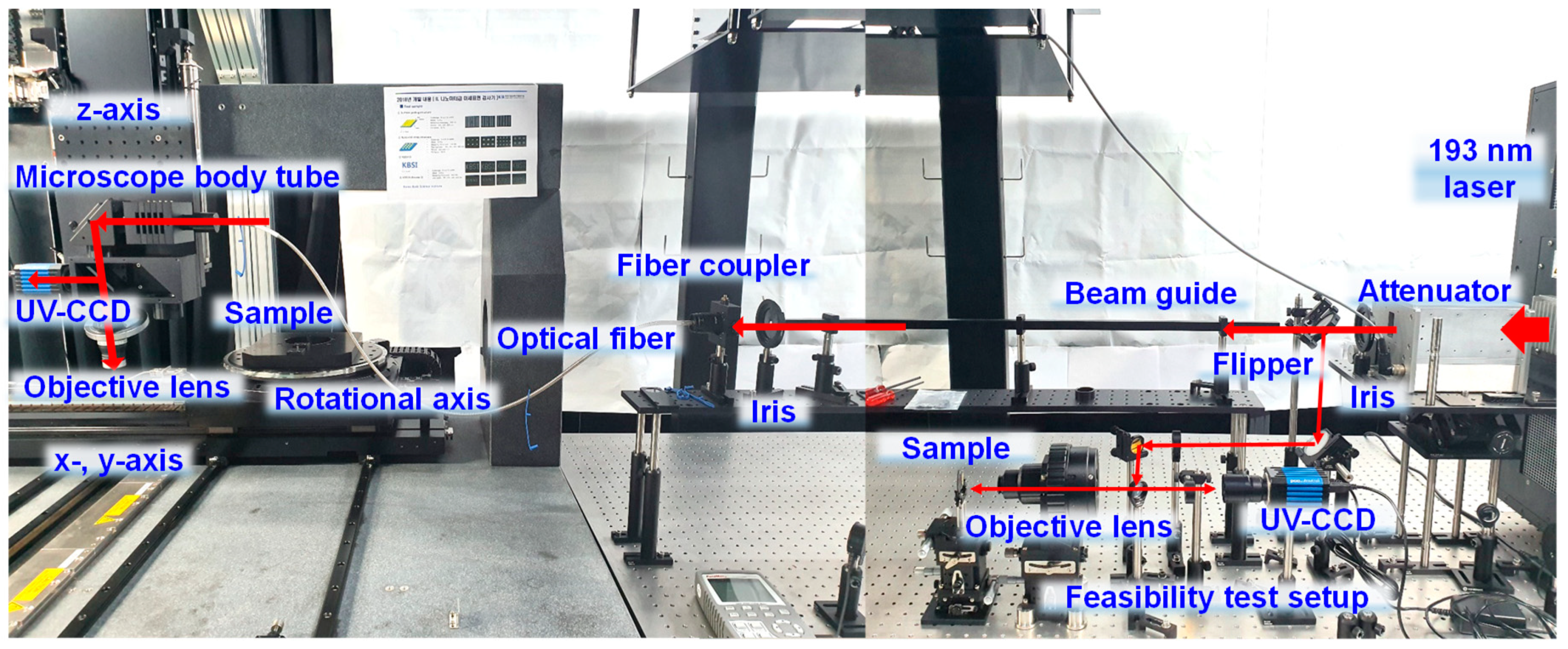
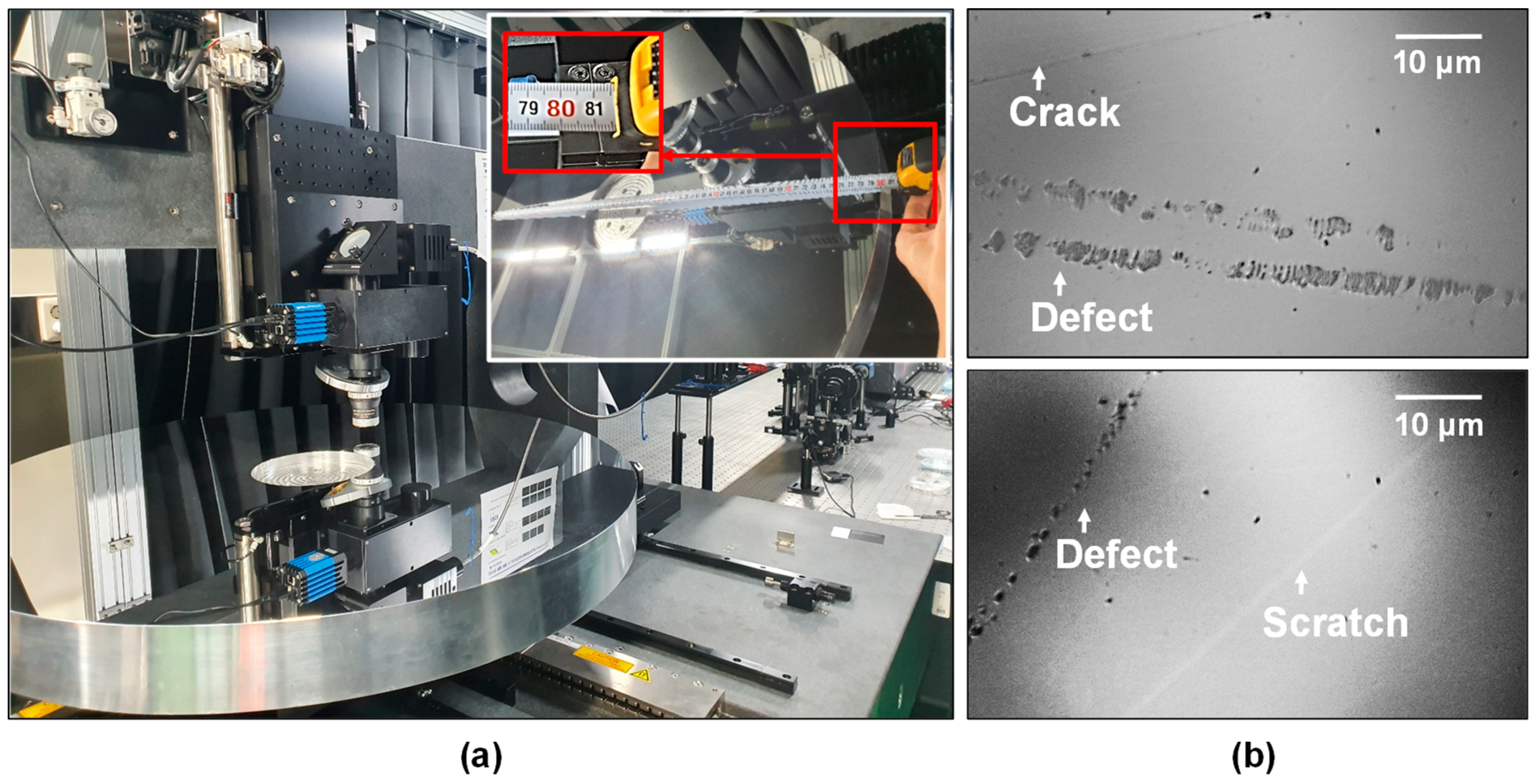
2. Materials and Methods
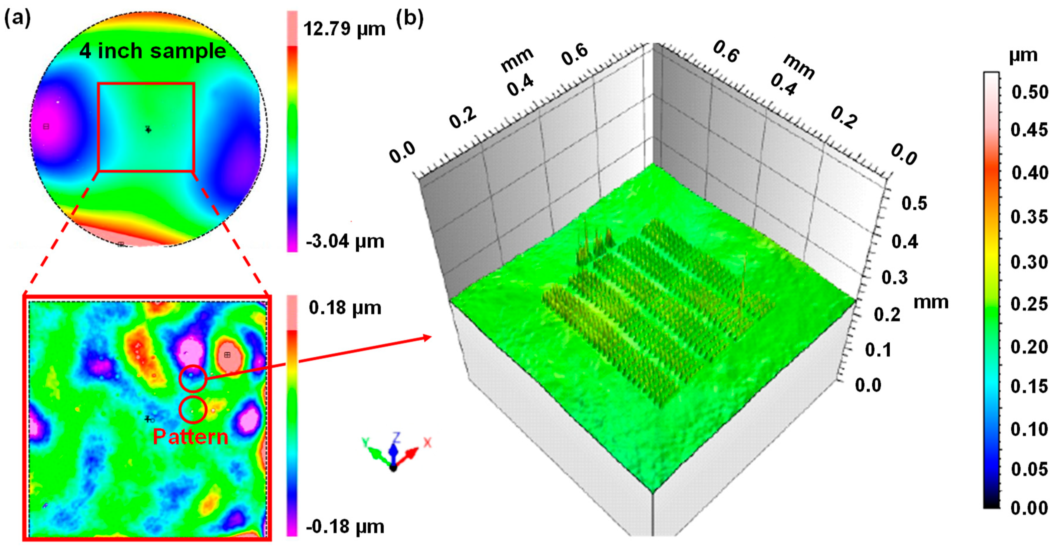
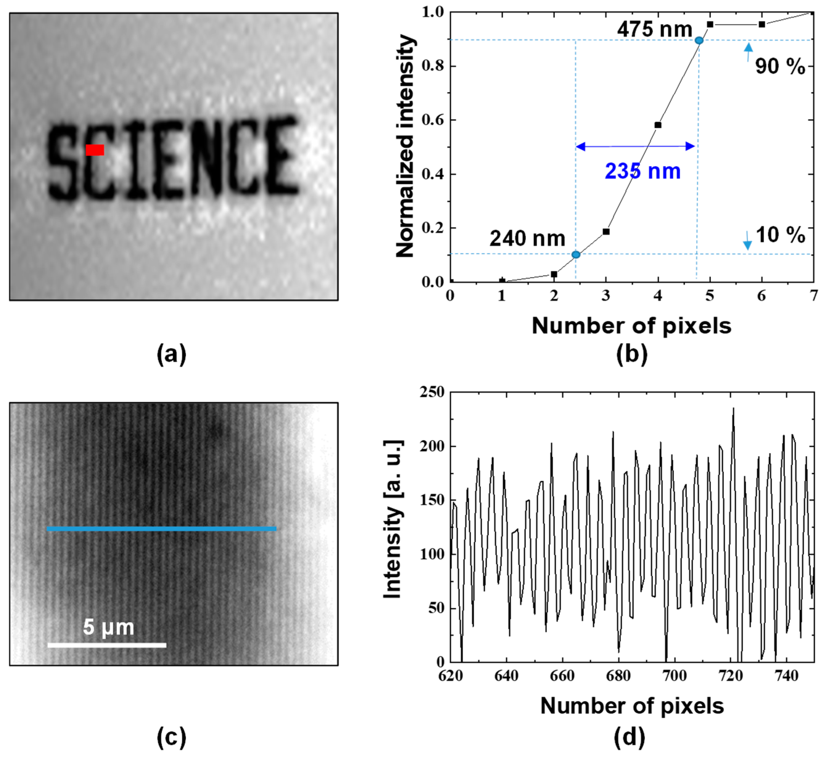
Figure 1 shows the experimental configuration of a 193-nm DUV microscope system based on the reflection mode. As shown in Figure 1a, this consists of a light source, beam control device (Figure 1b), microscope body tube (Figure 1c), sample stage (Figure 1d), and data processing computer.
An ArF excimer laser (Coherent, COMpex110) with a wavelength of 193 nm was used as the light source of the reflective DUV microscope. As shown in Figure 1b, the beam attenuator (Coherent, 2910218) was used to control the excimer laser output energy. Because the beam shape of the 193-nm excimer laser is rectangular type (24 mm (h) × 10 mm (w)), the first iris diaphragm was used to form an 8-mm diameter circular beam. Moreover, the fringe pattern that could be formed around the circular beam during the beam propagation along the beam guide is truncated by the second iris diaphragm. Then, the attenuated circular-shaped beam is entered into a fiber coupler to transfer it through the optical fiber to the microscope body tube that is one the most crucial components in the DUV microscope system. The optical fiber is specially manufactured for the 193-nm wavelength with a 1-mm core diameter and is designed for high energy transfer at up to 10 mJ/pulse.
Figure 1c shows the structure of the microscope body tube. The 193-nm laser beam propagated through the special optical fiber is enlarged to a size suitable for optical imaging through the beam expander. Because the numerical aperture (NA) of the optical fiber is 0.22, the beam with a diameter of 1 mm at the output of the optical fiber increases to 7.7 mm in diameter at the entrance of the beam expander, which is 21.8 mm in distance from the optical fiber output. The beam expander then forms an 18.5-mm diameter collimated beam at a distance of 200 mm from the beam expander output. The optical component cartridges are installed to control the beam energy additionally by using an neutral density filter. The beam reflected by the 45° reflective mirror is propagated into the 193-nm objective lens (Beck Optronic Solutions, Cassegrain-type reflecting objective) after passing through the beam splitter. The light reflected from the sample is propagated backwards; after reflection from the beam splitter, the beam is propagated into the UV-CCD (PCO, pco.ultraviolet) for high-resolution DUV microscope imaging.
Figure 1d shows a designed configuration of the stage system for the installation of the microscope body tube and the large optical surfaces, of the order of one meter in size. This system consists of several stages that move along the x, y, and rotational axes for the large optical sample and a stage that moves along the z axis for the microscope body tube. All components combined form a DUV microscope system capable of measuring up to a one-meter scale, of which each axis consists of a motion controller with a position accuracy of ±1 μm and a maximum movement speed of 100 mm/s. The microscope body tube creates a heavy load on the z-axis stage and the depth of focus of the objective lens is very short; thus, a counterbalance valve for precise z-axis adjustment was installed. Counterbalance valves are used in hydraulic systems working with overriding (running-away) or suspended loads. They are designed to create backpressure at the return line of the actuator to prevent losing control over the load. The detailed specifications for each stage are listed in Table 1. The uncertainty of the motion stage was verified through the experiment on the accuracy of the motion stage. Experimental verification of the stage was done with the displacement sensor in picoscale interferometers (Picoscale, Michelson interferometer). In Table 1, the specifications are presented, and the measurements obtained are compared for each stge. The differences in the measured movements of the motion stage presented in the Table 1 are small enough to have little influence on the imaging results obtained using the DUV microscope.
Figure 2 shows the full experimental configuration of the 193-nm DUV microscope based on the reflection imaging mode. The 193-nm excimer laser light is incident on the microscope body tube that is installed in the z-axis stage of the sample stage, after propagation through the beam attenuator, beam guide, fiber coupler, and optical fiber. After the light propagation in the microscope body tube, the light reflected from the sample is propagated into the UV-CCD. Independently, the feasibility setup using a flipper to switch beam direction is configured on the optical table to test the DUV microscope imaging before the full-scale application of the microscope system. This enables identification of the technical problems of the experimental configuration within a short time.
Figure 3 shows a side view of the structure of the sample pattern prepared for the evaluation of the spatial resolution of the 193-nm DUV microscope system. A 50-nm thick Au film was deposited on a 4-inch silicon substrate, and a 225-nm line-width 1D grating pattern and a 400-nm line-width alphabet pattern were fabricated using E-beam lithography. Such 1D grating patterns with a fill factor of 50% are designed for the evaluation of the spatial resolution of periodic structures, and the alphabet patterns are designed for the evaluation of the spatial resolution of defects or cracks.

3. Results

The characteristics of the 193-nm DUV microscope system are demonstrated by a comparison with commercial equipment used for optical surface inspection. For this, the aspherical stitching interferometer (ASI) based on Fizeau interference was used for the observation of surface figure, and the coherence correlation interferometer (CCI) based on white-light interferometer was used for the observation of surface roughness. The location of the defects (here, we consider the region where the fabricated alphabet patterns exist as defects) can be determined by measuring the surface figure of the sample using the ASI-Q (QED technology) instrument. As shown in Figure 4a, the red square indicates the area where the fabricated alphabet patterns are formed. Despite enlarging the image, it is still not possible to identify the patterns, because the lateral resolution of the ASI-Q is several µm at best. It is applied to quickly determine the position of the defects before the detailed imaging of the defects using the 193-nm DUV microscope system. Figure 4b shows the 3D image of several alphabet patterns observed inside a region measured using a CCI-optics (Taylor Hobson) instrument. Compared with Figure 4a, the enhanced image with high-resolution alphabet patterns is shown in a narrow area (0.825 mm × 0.825 mm). However, it is not sufficient to distinguish the pattern shapes, because it does not reach a spatial resolution high enough to recognize the shape of the alphabet pattern, when we consider the CCI with the lateral resolution of 0.76 μm.
Figure 5a shows the fabricated sample on the stage. The 4-inch sample is fixed on the sample stage and the bright spot (denoted by the red circle) presents the area where the patterns exist. Figure 5b shows the SEM images of the patterns. The SEM images were used to verify that the fabricated patterns were in good agreement with the designed patterns. Patterns with an average line width of 400 nm were used. Pattern imaging was carried out by two sequential processes using two objective lenses. First was wide-field imaging (field of view (FOV) = 625 μm × 467 μm) using an objective lens with NA 0.28 and second was detailed imaging (FOV = 135 μm × 100 μm) using an objective lens with NA 0.50. Figure 5c shows the pattern images of two cases, which clearly distinguish alphabet patterns with a line width of 400 nm.
The spatial resolution of the 193-nm DUV microscope imaging system was evaluated by analyzing the imaging results of the alphabet and 1D grating patterns. Figure 6a shows the DUV microscope image of alphabet patterns obtained with an NA 0.5 objective lens. In this condition, the pixel size was 100 nm. In this figure, the red bar is marked to investigate the spatial resolution of the pattern quantitatively. As a result, the spatial resolution at this position was estimated to be 235 nm by using the knife-edge method [21,22], as shown in Figure 6b. The normalized intensities of 10% and 90% with respect to the background intensity occur at 240 and 475 nm, respectively; thus, the spatial resolution is 235 nm when the intensity varies from 10% to 90%. This can be directly applied to detect defects and cracks on large-area optical components. Figure 6c shows the DUV microscope image of the 1D grating structure with a periodicity of 450 nm. The periodicity of 450 nm of the 1D grating structure and a line width of 225 nm are identified by analyzing this image. As shown in Figure 6d, the spatial resolution is confirmed to be 225 nm, when we consider the full width at half-maximum with respect to a certain single peak intensity distribution in the line profiles.
Figure 7 shows the results of the observation of defects/cracks present on the surface of a planar optical sample (manufactured with aluminum) with a diameter of 800 mm. Figure 7a shows the overall configuration to observe the defects that exist in the local area on the large optical surface using the DUV microscope, while Figure 7b presents clear images of the various kinds of defects, cracks, and scratches that can degrade the performance of large optics. Thus, our results show that this DUV microscope configuration allows imaging with a sub-μm resolution for large optical surfaces, which was not possible with conventional inspection equipment.

4. Conclusions

A 193-nm DUV microscope system applying the reflective mode was developed for the inspection of various defects and cracks on large optical surfaces, of the order of one meter in size. Direct observation was possible without sample preprocessing at room temperature and atmospheric pressure. In addition, the technique removes limitations on properties, such as optical material thickness and type, that exist for transmittive DUV microscopes. The sample imaging and achievable spatial resolution were verified using a 1D grating structure with a 225-nm line width. This DUV microscope system could be developed for applications as a cost-effective solution for quality control in the manufacturing of large optical elements. It is expected that this system can additionally be extended to nano/bio imaging.

Author Contributions

Supervision, I.J.K. and G.H.K.; investigation, H.-S.K. and I.J.K.; methodology, H.-S.K., I.J.K., D.-H.L., S.H., S.K.J. and J.G.P.; software, J.Y.B.; formal analysis, H.-S.K., I.J.K. and G.H.K.; writing, H.-S.K. and I.J.K.

Funding

This research was funded by CREATIVE CONVERGENCE RESEARCH PROJECT in the NATIONAL RESEARCH COUNCIL OF SCIENCE AND TECHNOLOGY OF KOREA, grant number CAP–15–01–KBSI and the KOREA BASIC SCIENCE INSTITUTE, grant number D39615.

Conflicts of Interest

The authors declare no conflict of interest.

References

  1. Briers, J.D. Interferometric testing of optical systems and components: A review. Opt. Laser Technol. 1972, 4, 28–41. [Google Scholar] [CrossRef]
  2. Kajava, T.T.; Lauranto, H.M.; Friberg, A.T. Interference pattern of the Fizeau interferometer. JOSA A 1994, 11, 2045–2054. [Google Scholar] [CrossRef]
  3. Goodwin, E.P.; Wyant, J.C. Field Guide to Interferometric Optical Testing; SPIE Press: Bellingham, WA, USA, 2006. [Google Scholar]
  4. Xu, Z.; Shilpiekandula, V.; Youcef-Toumi, K.; Yoon, S.F. White-light scanning interferometer for absolute nano-scale gap thickness measurement. Opt. Express 1994, 17, 15104–15117. [Google Scholar] [CrossRef]
  5. Flores, S.M.; Toca-Herrera, J.L. The new future of scanning probe microscopy: Combining atomic force microscopy with other surface-sensitive techniques, optical microscopy and fluorescence techniques. Nanoscale 2009, 1, 40–49. [Google Scholar] [CrossRef] [PubMed]
  6. Wang, J.; Lv, J.; Zhao, G.; Wang, G. Free-space laser communication system with rapid acquisition based on astronomical telescopes. Opt. Express 2015, 23, 20655–20667. [Google Scholar] [CrossRef]
  7. Siewert, F.; Buchheim, J.; Gwalt, G.; Bean, R.; Mancuso, A.P. On the characterization of a 1 m long ultra-precise KB-focusing mirror pair for European XFEL by means of slope measuring deflectometry. Rev. Sci. Instrum. 2019, 90, 021713. [Google Scholar] [CrossRef] [PubMed]
  8. Yu, T.J.; Lee, S.K.; Sung, J.H.; Yoon, J.W.; Jeong, T.M.; Lee, J. Generation of high-contrast, 30 fs, 1.5 PW laser pulses from chirped-pulse amplification Ti:sapphire laser. Opt. Express 2012, 20, 10807–10815. [Google Scholar] [CrossRef] [PubMed]
  9. Ye, R.; Chang, M.; Pan, C.S.; Chiang, C.A.; Gabayno, J.L. High-resolution optical inspection system for fast detection and classification of surface defects. Int. J. Optomechatronics 2018, 12, 1–10. [Google Scholar] [CrossRef]
  10. Chang, M.; Chou, Y.C.; Lin, P.T.; Gabayno, J.L. Fast and high-resolution optical inspection system for in-line detection and labeling of surface defects. CMC Comput. Mat. Contin. 2014, 42, 125–140. [Google Scholar]
  11. Cao, B.; Hoang, P.; Ahn, S.; Kang, H.; Kim, J.; Noh, J. High-speed focus inspection system using a position-sensitive detector. Sensors 2017, 17, 2842. [Google Scholar] [CrossRef] [PubMed]
  12. Abuazza, A.; Brabazon, D.; El-Baradie, M.A. Analysis of surface defects using a novel developed fiber-optics laser scanning system. J. Mater. Proc. Technol. 2003, 143, 875–879. [Google Scholar] [CrossRef]
  13. Hess, S.T.; Girirajan, T.P.; Mason, M.D. Ultra-high resolution imaging by fluorescence photoactivation localization microscopy. Biophys. J. 2006, 91, 4258–4272. [Google Scholar] [CrossRef]
  14. Hell, S.W.; Wichmann, J. Breaking the diffraction resolution limit by stimulated emission: Stimulated-emission-depletion fluorescence microscopy. Opt. Lett. 1994, 19, 780–782. [Google Scholar] [CrossRef]
  15. Bewersdorf, J.; Schmidt, R.; Hell, S.W. Comparison of I5M and 4Pi-microscopy. J. Microsc. 2006, 222, 105–117. [Google Scholar] [CrossRef] [PubMed]
  16. Schrader, M.; Hell, S.W. Three-dimensional super-resolution with a 4Pi-confocal microscope using image restoration. J. Appl. Phys. 1998, 84, 4033–4042. [Google Scholar] [CrossRef]
  17. Deitche, J.; Kempe, M.; Rudolph, W. Resolution in nonlinear laser scanning microscopy. J. Microsc. 1994, 174, 69–73. [Google Scholar] [CrossRef]
  18. Brunner, R.; Steiner, R.; Rudolf, K.; Dobschal, H.J. Diffractive-refractive hybrid microscope objective for 193 nm inspection systems. In Proceedings of the SPIE’s 48th Annual Meeting, San Diego, CA, USA, 10 November 2003; Volume 5177, pp. 9–15. [Google Scholar]
  19. Ehret, G.; Pilarski, F.; Bergmann, D.; Bodermann, B.; Buhr, E. A new high-aperture 193 nm microscope for the traceable dimensional characterization of micro-and nanostructures. Meas. Sci. Technol. 2009, 20, 084010. [Google Scholar] [CrossRef]
  20. Li, Z.; Pilarski, F.; Bergmann, D.; Bodermann, B. A Quantitative 193 nm DUV Microscope. In Proceedings of the Euspen International Conference, Delft, The Netherlands, 31 May–4 June 2010. [Google Scholar]
  21. Long, T.; Clement, S.W.; Bao, Z.; Wang, P.; Tian, D.; Liu, D. High spatial resolution and high brightness ion beam probe for in-situ elemental and isotopic analysis. Nucl. Instrum. Methods. Phys. Res. 2018, 419, 19–25. [Google Scholar] [CrossRef]
  22. Kim, H.T.; Kim, I.J.; Kim, C.M.; Jeong, T.M.; Yu, T.J.; Lee, S.K.; Sung, J.H.; Yoon, J.W.; Yun, H.; Jeon, S.C.; et al. Single-shot nanometer-scale holographic imaging with laser-driven x-ray laser. Appl. Phys. Lett. 2011, 98, 121105. [Google Scholar] [CrossRef]
Figure 1. Configuration of a 193-nm DUV microscope system based on the reflection mode. (a) Full configuration; (b) beam control stage; (c) microscope body tube; (d) four-axis controllable (x, y, z, and rotational stage) sample stage to control the large optical elements and microscope body tube.
Applsci 09 05205 g001
Figure 2. Full experimental configuration of the 193-nm DUV microscope system with the reflection imaging mode and the feasibility setup for test DUV microscope imaging.
Applsci 09 05205 g002
Figure 3. Sample design for the evaluation of the spatial resolution of the 193-nm DUV microscope system.
Applsci 09 05205 g003
Figure 4. Surface images of the alphabet patterns observed using ASI-Q and CCI-optics. (a) Surface image of 4-inch sample as shown in Figure 3 using ASI-Q. (b) Detailed 3D image of alphabet patterns on the sample using CCI-optics.
Applsci 09 05205 g004
Figure 5. (a) Pattern formation on the sample. (b) SEM images of alphabet patterns. (c) DUV microscope images of alphabet patterns using NA 0.28 and NA 0.5 objective lenses.
Applsci 09 05205 g005
Figure 6. (a) DUV microscope image of alphabet patterns. (b) Normalized intensity as a function of the number of pixels on the red bar denoted in Figure 6a. (c) DUV microscope image of 1D grating patterns. (d) Line profile of the intensity as a function of number of pixels on the blue line in Figure 6c.
Applsci 09 05205 g006
Figure 7. (a) Overall configuration to observe the defects present on the surface of a planar optical sample that has a diameter of 800 mm. (b) Result of the inspection of a local area, showing the defects, cracks, and scratches identified.
Applsci 09 05205 g007
Table 1. Performance indices for each axis of the sample stage. Specification and measurement results are compared.
AxisXYZR
TypeSpec.Meas.Spec.Meas.Spec.Meas.Spec.Meas.
ActuatorLinear motorLinear motorLinear motor + counterbalanceDirect drive motor
Max. travel length (mm)600600600600300290360°360°
Max. velocity
(mm/s)
10010010010010010030°/s30°/s
Resolution
(nm)
≤ 54.88≤ 54.88≤ 54.88≤ 0.01°≤ 0.01°
Position accuracy (μm)± 1.0± 0.3± 1.0± 0.3± 0.5± 0.3--
Bi-dir. repeatability
(μm)
± 0.5± 0.2± 0.5± 0.25± 0.3± 0.3≤ 0.05°≤ 0.05°
In-position stability (nm)± 100± 29± 100± 41± 100±83--
Spec.: specification, Meas.: measurement, Max.: maximum, Dir.: directional.

