Article

Reduction of Schottky Barrier Height at Graphene/Germanium Interface with Surface Passivation

Univ Rennes, CNRS, IPR (Institut de Physique de Rennes)—UMR 6251, F-35000 Rennes, France
*
Author to whom correspondence should be addressed.
Appl. Sci. 2019, 9(23), 5014; https://doi.org/10.3390/app9235014
Submission received: 29 October 2019 / Revised: 10 November 2019 / Accepted: 14 November 2019 / Published: 21 November 2019

Abstract

:
Fermi level pinning at metal/semiconductor interfaces forbids a total control over the Schottky barrier height. 2D materials may be an interesting route to circumvent this problem. As they weakly interact with their substrate through Van der Waals forces, deposition of 2D materials avoids the formation of the large density of state at the semiconductor interface often responsible for Fermi level pinning. Here, we demonstrate the possibility to alleviate Fermi-level pinning and reduce the Schottky barrier height by the association of surface passivation of germanium with the deposition of 2D graphene.

1. Introduction

Combinations of two-dimensional materials and bulk three-dimensional semiconductors have gained considerable attention lately, owing to potential new device concepts. Most studies focused on the properties of graphene/silicon (G/Si) Schottky junctions [1]. Many different new functionalities were observed such as bias-controlled Schottky barrier height [2,3] (SBH), photodetectors [4,5,6,7,8,9] or solar cells [10,11,12]. When covered with a metal, Metal/G/Si can be used as an efficient spin injector [13,14] or a low-resistance contact [15,16]. The reduction of the Si SBH is made possible by simultaneous etching of the silicon oxide and hydrogen passivation of the surface with graphene already on top [17]. In that case, the hydrogen passivation of Si is protected during metallization. This results in alleviation of the Fermi-level (FL) pinning and a low SBH. It is, therefore, possible to strongly reduce the SBH and associated contact resistance on moderately doped Si without any thermal treatment, or heavy doping at the interface.
Because of similar FL pinning issues, it is very challenging to realize low-resistance contacts to n-type Ge. Reduction of the SBH is particularly important for the realization of ohmic contacts or for impedance matching for spin injection [18,19]. In order to alleviate the FL pinning, different strategies such as Ge surface passivation through wet chemicals [20,21] or deposition of a thin insulator layer on Ge surfaces have been employed [22,23,24,25,26,27].
The aim of this work is to obtain a low SBH for electrons in graphene/Ge junctions using a similar strategy as for graphene/Si junctions: to associate graphene with surface passivation of the semiconductor in order to alleviate FL pinning and reduce the SBH. For that purpose, we used X-ray Photoemission Spectroscopy (XPS) to study the interface between physico-chemistry and band alignments of graphene/germanium contacts and to show the possibility to modify the SBH via wet chemical passivation of the underlying germanium. We then observed the effect of the modification of the graphene work function by gold deposition on the SBH of the junction.

2. Materials and Methods
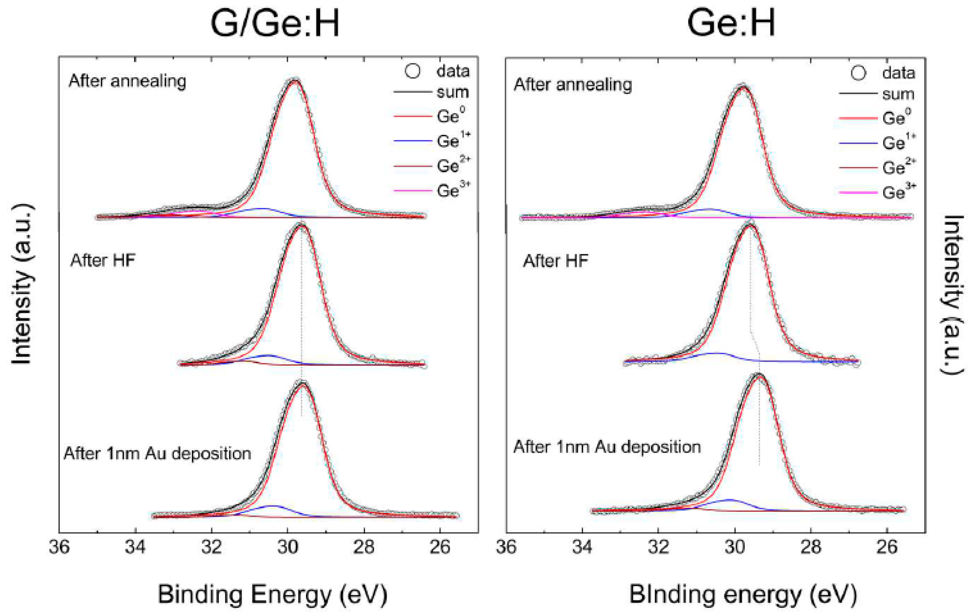
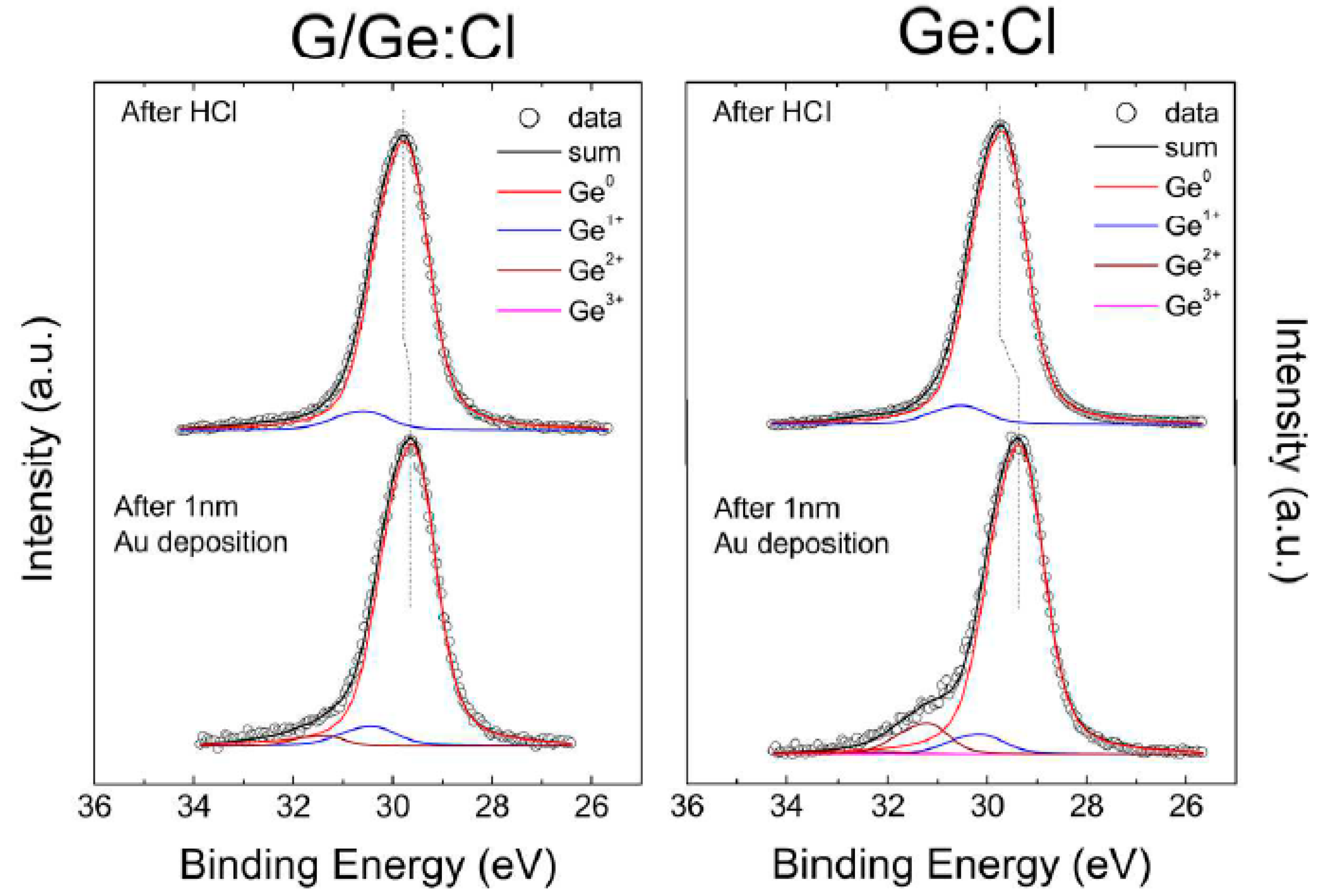
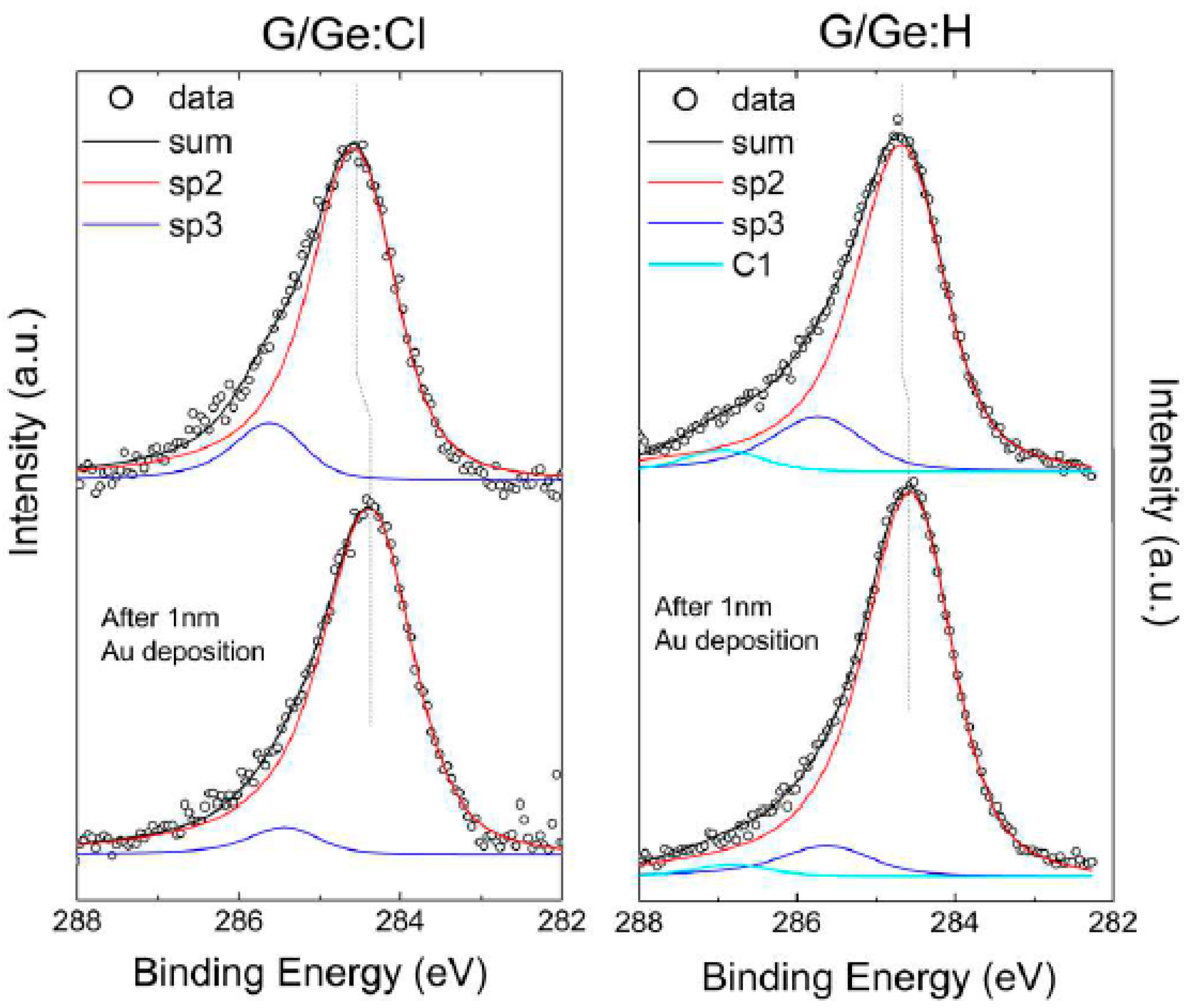
Intrinsic Ge (001) samples were degreased in ethanol for 30 min, then successively dipped in a dilute HCl bath (HCl:H2O, 1:4) for 30 s and a H2O2 bath (H2O2:H2O, 1:10) for 60 s, three times each. The surface oxide was then etched one last time in HCl followed by a final oxidizing step in NH4OH:H2O2:H2O (1:2:10). For the realization of graphene/germanium contacts, monolayer CVD-graphene grown on Cu was purchased from Graphenea®. A 200 nm polymethyl methacrylate (PMMA) layer was spin-coated on top of the G/Cu to serve as a mechanical support layer during transfer. The Cu was then etched in a FeCl3 solution until no Cu could be seen and the floating PMMA/G was rinsed in several water and diluted HCl baths in order to eliminate metallic residues. After rinsing, the PMMA/G was transferred onto the Ge wafer and left to dry overnight. After transfer and drying, the PMMA resist was cleaned in acetone and the sample was introduced under ultra-high vacuum (UHV) with a base pressure of 10−10 Torr for a 3 h annealing at 300 °C in order to remove resist residues. After annealing, the sample was taken out of UHV for a wet passivation step either in HF (10%) for 10 min for hydrogen passivation (hereafter named Ge:H) or in dilute 7.5% HCl for 30 s for Cl passivation (hereafter named Ge:Cl).
We used X-ray photoemission spectroscopy (XPS) to study the physico-chemistry of the G/Ge contacts with different Ge surface treatments before and after gold deposition. Measurements were realized at normal emission and room temperature using a MgKα (1253.6 eV) X-ray source. The kinetic energy of the emitted electrons was measured by employing a hemispherical analyzer (Omicron EA125) with a five-channel detection system. The total energy resolution was 0.80 eV. Before photoemission measurement, the analyzer was calibrated with a thick gold sample. We assume an energy difference of 84.0 eV between the Au4f7/2 peak and the Fermi level [28].

3. Results

Figure 1 shows the Ge3d core level after 3 h annealing in UHV for the G/Ge samples. The experimental spectra were decomposed after background correction with a least-square procedure using a Lorentzian convoluted with a Gaussian to represent each of the spin–orbit-split components of the Ge3d core level. In the fitting procedure, the spin–orbit splitting of the Ge3d core level was fixed at 0.58 eV and the branching ratio was taken to be the statistical value of 3:2. The same spin–orbit-split and branching ratio were used for the various components introduced in our fitting procedure. The main peak at 29.64eV for G/Ge and 29.60eV for Ge is attributed to bulk Ge. Other peaks located at 0.9 eV, 1.6 eV, 2.6 eV and 3.4 eV from the main peak correspond to the photoemission signal from germanium in an oxidation state of +1, +2, +3 and +4, respectively [29].
After HF etching, only the +1 oxidation component is observable for the Ge sample, while for G/Ge the +1 and +2 oxidation states are visible. This indicates that HF removed most of the oxide but that the etching efficiency and/or kinetics in HF are reduced by the presence of graphene on the surface in opposition to what we observed on silicon, where oxide removal is not affected by the presence of graphene [17]. The deposition of 1 nm Au on the Ge surface induces a 0.25 eV shift of the main Ge3d component towards lower binding energies (BE). This shift indicates that the gold deposition induces a band bending change as the Au/Ge interface forms. For the graphene-covered sample, no binding energy shift was observed after the deposition of gold, indicating that no further band bending took place.
Because of the greater bond strength of Ge–Cl over Ge–H, chloride passivation is expected to be more stable than hydrogen [30]. As Ge oxides are soluble in HCl, etching in HCL would remove the oxide and passivate the surface with chloride. We can see in Figure 2 an almost similar shape of the Ge3d spectra between graphene-covered and -uncovered surfaces. Here, in the photoemission spectra, we observe only a contribution from Ge atoms in oxidation state +1 in addition to the Ge bulk component. This indicates that either the oxide removal is not complete in HCl or the surface re-oxidizes before introduction under UHV. We confirm in our survey spectrum that Cl ions are still present at the surface after introduction of the sample in UHV. After the deposition of 1 nm Au on the Ge:Cl surface, we observe a 0.34 eV shift towards lower binding energies of the Ge3d bulk component. The final BE position of the main Ge3d peak is essentially the same as for the Au/Ge:H sample. When the surface is protected with graphene the shift of the Ge3d main component is only 0.19 eV.
Figure 3 shows the experimental spectrum of the C1s core level for single-layer graphene on Ge passivated with HCl and HF. A main component corresponds to C–C sp2 bonds and a second component located at 0.7 eV higher BE is attributed to sp3 carbons [31]. One more component at a 2.4 eV higher BE (labelled C1 on the figure) is assigned to the contribution of carbon atoms from PMMA residues [32]. It can be seen that the deposition of 1 nm of Au on graphene causes a C1s core level shift towards lower BE of 0.18 and 0.10 eV for Ge:Cl and Ge:H samples, respectively. This shift is induced by an electron transfer from graphene toward Au at the graphene/Au interface [33].

4. Discussion

From the position of the main Ge3d peak, we can determine the Schottky barrier height for electrons, defined as the difference in energy between the Fermi level and the conduction band minimum at the interface, with the following equation:
ϕ B = ( Δ ( V B G e 3 d ) + E g ) B E G e 3 d
where Δ ( V B G e 3 d ) is the energy difference between the Ge3d core level and the valence band, E g is the Ge bandgap and B E ( G e 3 d ) is the measured binding energy of the Ge3d core level referenced to the Fermi level. Δ ( V B G e 3 d ) is set to 29.30 eV [25] and the Ge bandgap to 0.67 eV. The measured SBHs are summarized in Table 1 as a function of the surface treatment.
Table 1 summarizes the SBH of our heterostructures with different surface treatments with and without graphene and before and after Au deposition. We can notice that the SBH of intimate Au/Ge interfaces is independent of the Ge surface treatment. These SBH values are close to previous reports for Au/Ge contacts [34]. For metal/Ge interfaces, the FL is strongly pinned close to the valence band edge. Indeed the SBH only weakly depends on the metal work function ranging from 0.49 to 0.67 eV for metal work functions variations of 2.8 eV [35]. The introduction of a graphene monolayer between Au and Ge strongly reduces the SBH to about 0.5 eV. This behavior suggests that the FL pinning was alleviated by the presence of graphene at the interface.
An even lower SBH value of 0.31 eV was obtained for graphene on a HCl-treated Ge surface. This is a strong indication that the chloride passivation was efficient in reducing the surface state density and that the FL is not pinned. In that case, we can apply the simple model of Schottky–Mott where the SBH ϕ B is:
ϕ B = W G χ Ge
with W G the work function of graphene and χ Ge the electronic affinity of the semiconductor. Lin et al. [36] measured a W G of 4.3 eV for CVD-graphene deposited via a PMMA-assisted method similar to ours. This value is lower than the commonly used 4.54 eV because of resist contamination and structural defects induced during wet transfer. With an electron affinity of 4.0 eV for Ge, this would lead to an SBH of 0.30 eV, in excellent agreement with our result. For an un-passivated surface, the FL is expected to be pinned close to the charge neutrality level (0.09 eV above the valence band maximum [35]). In that case, Dimoulas et al. [35] predict an SBH of 0.56 eV for a graphene/Ge contact. The SBH for G/Ge:H is between these two values, suggesting a less efficient passivation of HF compared to HCl. This is expected since the hydrogen passivation is not stable in air and hydrogen is removed from the surface within a few minutes [37]. Xu et al. [38] showed on G/Si:H that the dominant interaction between graphene- and hydrogen-passivated Si surfaces is through Van der Waals forces. In that case, C and Si atoms do not interact with each other. Depassivation of Si induced a stronger interaction between Si and C atoms, eventually leading to the formation of covalent bonds and an increased density of states in the gap of Si. The situation is similar here, with a weak interaction between C and Ge atoms associated with a low density of states in the Ge bandgap when passivation is efficient (Cl-passivation). When the passivation is less efficient (H-passivation), the interaction between C and Ge atoms becomes stronger and the density of states in the Ge gap increases.
As gold is deposited on the G/Ge:Cl surface, the SBH increases by 0.19 eV. At the same time, the work function of graphene is increased by an almost similar value of 0.18 eV. This is another strong indication that the FL is unpinned at the Ge surface. A similar gold deposition weakly modifies the SBH for G/Ge:H, supporting our interpretation of a more pinned FL due to a less efficient hydrogen passivation.

5. Conclusions

We studied the physico-chemistry and band alignments of G/Ge surfaces with different passivation treatments of the Ge surface by photoemission spectroscopy. We observed an almost complete removal of the surface oxides by wet chemical etching in HF or HCl. These wet etchings were efficient even with the graphene layer on the surface. When Au is deposited on Ge, the SBH is essentially independent of the surface treatment, as expected for strongly pinned FL at metal/Ge contacts. We observe a reduction of the SBH by the insertion of a graphene monolayer between Au and Ge, suggesting an alleviation of the FL. An even stronger alleviation is induced by chloride passivation. In that case, we reach the Schottky limit. The association of graphene with an efficient surface passivation could lead to a low SBH on n-type Ge.

Author Contributions

Conceptualization, J.C. and J.-C.L.B.; Data curation, J.C. and J.-C.L.B.; Formal analysis, J.C., A.M. and J.-C.L.B.; Funding acquisition, P.S. and J.-C.L.B.; Investigation, J.-C.L.B.; Methodology, J.C., G.D., B.L., P.S. and J.-C.L.B.; Project administration, P.T., P.S. and J.-C.L.B.; Resources, S.T.; Supervision, P.S. and J.-C.L.B.; Validation, J.-C.L.B.; Writing—original draft, J.-C.L.B.; Writing—review & editing, P.S.

Funding

This research was funded by the Agence Nationale de la Recherche (ANR). We acknowledge the support from the French National Research Agency (ANR) FEOrgSpin project (Grant No. ANR-18-CE24-0017-01).

Conflicts of Interest

The authors declare no conflict of interest.

References

  1. Di Bartolomeo, A. Graphene Schottky Diodes: An Experimental Review of the Rectifying Graphene/Semiconductor Heterojunction. Phys. Rep. 2016, 606, 1–58. [Google Scholar] [CrossRef]
  2. Yang, H.; Heo, J.; Park, S.; Song, H.J.; Seo, D.H.; Byun, K.-E.; Kim, P.; Yoo, I.; Chung, H.-J.; Kim, K. Graphene Barristor, a Triode Device with a Gate-Controlled Schottky Barrier. Science 2012, 336, 1140–1143. [Google Scholar] [CrossRef] [PubMed]
  3. Ojeda-Aristizabal, C.; Bao, W.; Fuhrer, M.S. Thin-Film Barristor: A Gate-Tunable Vertical Graphene-Pentacene Device. Phys. Rev. B Condens. Matter Mater. Phys. 2013, 88, 3–6. [Google Scholar] [CrossRef]
  4. An, Y.; Behnam, A.; Pop, E.; Ural, A. Metal-Semiconductor-Metal Photodetectors Based on Graphene/p-Type Silicon Schottky Junctions. Appl. Phys. Lett. 2013, 102, 013110. [Google Scholar] [CrossRef]
  5. Goykhman, I.; Sassi, U.; Desiatov, B.; Mazurski, N.; Milana, S.; De Fazio, D.; Eiden, A.; Khurgin, J.; Shappir, J.; Levy, U.; et al. On-Chip Integrated, Silicon-Graphene Plasmonic Schottky Photodetector with High Responsivity and Avalanche Photogain. Nano Lett. 2016, 16, 3005–3013. [Google Scholar] [CrossRef]
  6. Casalino, M.; Sassi, U.; Goykhman, I.; Eiden, A.; Lidorikis, E.; Milana, S.; De Fazio, D.; Tomarchio, F.; Iodice, M.; Coppola, G.; et al. Vertically Illuminated, Resonant Cavity Enhanced, Graphene-Silicon Schottky Photodetectors. ACS Nano 2017, 11, 10955–10963. [Google Scholar] [CrossRef]
  7. Amirmazlaghani, M.; Raissi, F.; Habibpour, O.; Vukusic, J.; Stake, J. Graphene-Si Schottky IR Detector. IEEE J. Quantum Electron. 2013, 49, 589–594. [Google Scholar] [CrossRef]
  8. Luongo, G.; Giubileo, F.; Genovese, L.; Iemmo, L.; Martucciello, N.; Di Bartolomeo, A. I-V and C-V Characterization of a High-Responsivity Graphene/Silicon Photodiode with Embedded MOS Capacitor. Nanomaterials 2017, 7, 158. [Google Scholar] [CrossRef]
  9. Luongo, G.; Di Bartolomeo, A.; Giubileo, F.; Chavarin, C.A.; Wenger, C. Electronic Properties of Graphene/p-Silicon Schottky Junction. J. Phys. D Appl. Phys. 2018, 51, 255305. [Google Scholar] [CrossRef]
  10. Li, X.; Zhu, H.; Wang, K.; Cao, A.; Wei, J.; Li, C.; Jia, Y.; Li, Z.; Li, X.; Wu, D. Graphene-on-Silicon Schottky Junction Solar Cells. Adv. Mater. 2010, 22, 2743–2748. [Google Scholar] [CrossRef]
  11. Miao, X.; Tongay, S.; Petterson, M.K.; Berke, K.; Rinzler, A.G.; Appleton, B.R.; Hebard, A.F. High Efficiency Graphene Solar Cells by Chemical Doping. Nano Lett. 2012, 12, 2745–2750. [Google Scholar] [CrossRef]
  12. Song, Y.; Li, X.; Mackin, C.; Zhang, X.; Fang, W.; Palacios, T.; Zhu, H.; Kong, J. Role of Interfacial Oxide in High-Efficiency Graphene-Silicon Schottky Barrier Solar Cells. Nano Lett. 2015, 15, 2104–2110. [Google Scholar] [CrossRef]
  13. Van’t Erve, O.M.J.; Friedman, A.L.; Cobas, E.; Li, C.H.; Robinson, J.T.; Jonker, B.T. Low-Resistance Spin Injection into Silicon Using Graphene Tunnel Barriers. Nat. Nanotechnol. 2012, 7, 737–742. [Google Scholar] [CrossRef]
  14. Van’t Erve, O.M.J.; Friedman, A.L.; Cobas, E.; Li, C.H.; Hanbicki, A.T.; McCreary, K.M.; Robinson, J.T.; Jonker, B.T. A Graphene Solution to Conductivity Mismatch: Spin Injection from Ferromagnetic Metal/Graphene Tunnel Contacts into Silicon. J. Appl. Phys. 2013, 113, 17C502. [Google Scholar] [CrossRef]
  15. Lee, M.H.; Cho, Y.; Byun, K.E.; Shin, K.W.; Nam, S.G.; Kim, C.; Kim, H.; Han, S.A.; Kim, S.W.; Shin, H.J.; et al. Two-Dimensional Materials Inserted at the Metal/Semiconductor Interface: Attractive Candidates for Semiconductor Device Contacts. Nano Lett. 2018, 18, 4878–4884. [Google Scholar] [CrossRef]
  16. Courtin, J.; Le Gall, S.; Chretien, P.; Moréac, A.; Delhaye, G.; Lépine, B.; Tricot, S.; Turban, P.; Schieffer, P.; Le Breton, J.-C. Low Schottky Barrier Height and Transport Mechanism in Gold-Graphene-Silicon (001) Heterojunctions. Nanoscale Adv. 2019, 1, 3372–3378. [Google Scholar] [CrossRef]
  17. Le Breton, J.C.; Tricot, S.; Delhaye, G.; Lépine, B.; Turban, P.; Schieffer, P. Band Alignments in Fe/Graphene/Si (001) Junctions Studied by x-Ray Photoemission Spectroscopy. Appl. Phys. Lett. 2016, 109, 051601. [Google Scholar] [CrossRef]
  18. Cantoni, M.; Petti, D.; Rinaldi, C.; Bertacco, R. Bandstructure Line-up of Epitaxial Fe/MgO/Ge Heterostructures: A Combined x-Ray Photoelectron Spectroscopy and Transport Study. Appl. Phys. Lett. 2011, 98, 032104. [Google Scholar] [CrossRef]
  19. Jain, A.; Louahadj, L.; Peiro, J.; Le Breton, J.C.; Vergnaud, C.; Barski, A.; Beigné, C.; Notin, L.; Marty, A.; Baltz, V.; et al. Electrical Spin Injection and Detection at Al2O3/n-Type Germanium Interface Using Three Terminal Geometry. Appl. Phys. Lett. 2011, 99, 162102. [Google Scholar] [CrossRef]
  20. Thathachary, A.V.; Bhat, K.N.; Bhat, N.; Hegde, M.S. Fermi Level Depinning at the Germanium Schottky Interface through Sulfur Passivation. Appl. Phys. Lett. 2010, 96, 152108. [Google Scholar] [CrossRef]
  21. Maeda, T.; Takagi, S.; Ohnishi, T.; Lippmaa, M. Sulfur Passivation of Ge (0 0 1) Surfaces and Its Effects on Schottky Barrier Contact. Mater. Sci. Semicond. Process. 2006, 9, 706–710. [Google Scholar] [CrossRef]
  22. Roy, A.M.; Lin, J.Y.J.; Saraswat, K.C. Specific Contact Resistivity of Tunnel Barrier Contacts Used for Fermi Level Depinning. IEEE Electron Device Lett. 2010, 31, 1077–1079. [Google Scholar] [CrossRef]
  23. Roy, A.M.; Lin, J.; Saraswat, K.C. The Effect of Fixed Charge in Tunnel-Barrier Contacts for Fermi-Level Depinning in Germanium. IEEE Electron Device Lett. 2012, 33, 761–763. [Google Scholar] [CrossRef]
  24. Zhou, Y.; Ogawa, M.; Han, X.; Wang, K.L. Alleviation of Fermi-Level Pinning Effect on Metal/Germanium Interface by Insertion of an Ultrathin Aluminum Oxide. Appl. Phys. Lett. 2008, 93, 202105. [Google Scholar] [CrossRef]
  25. Nishimura, T.; Kita, K.; Toriumi, A. A Significant Shift of Schottky Barrier Heights at Strongly Pinned Metal/Germanium Interface by Inserting an Ultra-Thin Insulating Film. Appl. Phys. Express 2008, 1, 051406. [Google Scholar] [CrossRef]
  26. Khurelbaatar, Z.; Kil, Y.H.; Yun, H.J.; Shim, K.H.; Nam, J.T.; Kim, K.S.; Lee, S.K.; Choi, C.J. Modification of Schottky Barrier Properties of Au/n-Type Ge Schottky Barrier Diode Using Monolayer Graphene Interlayer. J. Alloys Compd. 2014, 614, 323–329. [Google Scholar] [CrossRef]
  27. Kobayashi, M.; Kinoshita, A.; Saraswat, K.; Wong, H.S.P.; Nishi, Y. Fermi Level Depinning in Metal/Ge Schottky Junction for Metal Source/Drain Ge Metal-Oxide-Semiconductor Field-Effect-Transistor Application. J. Appl. Phys. 2009, 105, 023702. [Google Scholar] [CrossRef]
  28. Seah, M.P. Letters to the Editor. Surf. Interface Anal. 1989, 14, 488. [Google Scholar] [CrossRef]
  29. Schmeisser, D.; Schnell, R.D.; Bogen, A.; Himpsel, F.J.; Rieger, D.; Landgren, G.; Morar, J.F. Surface Oxidation States of Germanium. Surf. Sci. 1986, 172, 455–465. [Google Scholar] [CrossRef]
  30. Lu, Z.H. Air-Stable Cl-Terminated Ge(111). Appl. Phys. Lett. 1995, 68, 520–522. [Google Scholar] [CrossRef]
  31. Nikitin, A.; Näslund, L.-Å.; Zhang, Z.; Nilsson, A. C–H Bond Formation at the Graphite Surface Studied with Core Level Spectroscopy. Surf. Sci. 2008, 602, 2575–2580. [Google Scholar] [CrossRef]
  32. Cunge, G.; Ferrah, D.; Petit-Etienne, C.; Davydova, A.; Okuno, H.; Kalita, D.; Bouchiat, V.; Renault, O. Dry Efficient Cleaning of Poly-Methyl-Methacrylate Residues from Graphene with High-Density H2 and H2-N2 Plasmas. J. Appl. Phys. 2015, 118, 123302. [Google Scholar] [CrossRef]
  33. Giovannetti, G.; Khomyakov, P.; Brocks, G.; Karpan, V.; van den Brink, J.; Kelly, P. Doping Graphene with Metal Contacts. Phys. Rev. Lett. 2008, 101, 026803. [Google Scholar] [CrossRef]
  34. Lieten, R.R.; Afanas’ev, V.V.; Thoan, N.H.; Degroote, S.; Walukiewicz, W.; Borghs, G. Mechanisms of Schottky Barrier Control on N-Type Germanium Using Ge3N4interlayers. J. Electrochem. Soc. 2011, 158, 358–362. [Google Scholar] [CrossRef]
  35. Dimoulas, A.; Tsipas, P.; Sotiropoulos, A.; Evangelou, E.K. Fermi-Level Pinning and Charge Neutrality Level in Germanium. Appl. Phys. Lett. 2006, 89, 12–15. [Google Scholar] [CrossRef]
  36. Lin, W.-H.; Chen, T.-H.; Chang, J.-K.; Taur, J.-I.; Lo, Y.-Y.; Lee, W.-L.; Chang, C.-S.; Su, W.-B.; Wu, C.-I. A Direct and Polymer-Free Method for Transferring Graphene Grown by Chemical Vapor Deposition to Any Substrate. ACS Nano 2014, 8, 1784–1791. [Google Scholar] [CrossRef]
  37. Rivillon, S.; Chabal, Y.J.; Amy, F.; Kahn, A. Hydrogen Passivation of Germanium (100) Surface Using Wet Chemical Preparation. Appl. Phys. Lett. 2005, 87, 253101. [Google Scholar] [CrossRef]
  38. Xu, Y.; He, K.T.; Schmucker, S.W.; Guo, Z.; Koepke, J.C.; Wood, J.D.; Lyding, J.W.; Aluru, N.R. Inducing Electronic Changes in Graphene through Silicon (100) Substrate Modification. Nano Lett. 2011, 11, 2735–2742. [Google Scholar] [CrossRef]
Figure 1. Ge3d core level of G/Ge:H and Ge:H samples after annealing for 3 h under vacuum, after 10 mins in HF (10%) and after 1 nm Au deposition.
Applsci 09 05014 g001
Figure 2. Ge3d core level of G/Ge:Cl and Ge:Cl samples after 30 s in HCl (7.5%) and after 1 nm Au deposition.
Applsci 09 05014 g002
Figure 3. C1s core level of the graphene-covered regions for HF- and HCl-passivated Ge surfaces before and after 1 nm Au deposition.
Applsci 09 05014 g003
Table 1. Schottky Barrier Height (in eV) for various Ge surface treatments.
Surface TreatmentG/GeAu/G/GeAu/Ge
HF0.490.530.78
HCl0.310.500.77

