Article

Two-Step Plasma Treatment on Sputtered and Electroplated Cu Surfaces for Cu-To-Cu Bonding Application

1
Graduate School of Nano-IT Design Convergence, Seoul National University of Science and Technology, Seoul 01811, Korea
2
Department of Mechanical Engineering, Seoul National University of Science and Technology, Seoul 01811, Korea
*
Author to whom correspondence should be addressed.
Appl. Sci. 2019, 9(17), 3535; https://doi.org/10.3390/app9173535
Submission received: 2 August 2019 / Revised: 26 August 2019 / Accepted: 26 August 2019 / Published: 28 August 2019

Abstract

:

Featured Application

3D packaging, Flip chip packaging.

Abstract

The technology trends of next generation electronic packaging are moving toward heterogeneous 3D packaging systems. One of the key processes of 3D packaging system is Cu-to-Cu bonding, which is highly dependent on the planarized, activated, and oxygen-free Cu surface. A two-step plasma treatment is studied to form a Cu surface that does not react with oxygen and improves the Cu bonding interface quality at low bonding temperature (300 °C). In this study, the effects of two-step plasma treatment on both sputtered and electroplated Cu surfaces were evaluated through structural, chemical, and electrical analysis. The Cu bonding interface was studied by scanning acoustic tomography analysis after the thermocompression bonding process. Both sputtered and electroplated Cu thin films had the preferred orientation of (111) plane, but sputtered Cu exhibited larger grains than the electroplated Cu. As a result, the roughness of sputtered Cu was lower, and the resistivity was higher than that of electroplated Cu. Based on X-ray photoelectron spectroscopy analysis, the sputtered Cu formed more copper nitrides and fewer copper oxides than the electroplated Cu. A significant improvement in bonding quality at the Cu bonded interface was observed in sputtered Cu.

1. Introduction

3D packaging is becoming a core advanced packaging technology because of its improved performance, effective power delivery, efficient signal integrity, small form factor, and heterogeneous packaging [1,2,3]. However, there are still technological challenges to be resolved such as thermal management, design and methodology, yield, electrical testing and reliability. In 3D packaging, there are three ways to stack devices such as die stacking, wafer stacking and package stacking. Die stacking can offer higher yield, but medium performance improvement, and wafer stacking give the highest performance with the lowest cost possible, but a cost with this methodology depends on a compound yield. Lastly, package stacking provides higher yield, but lower performance improvement and the highest cost [1]. In order to construct a stacked device structure, TSV (through Si via) forming, Si wafer thinning, and wafer or chip bonding processes are needed. In many bonding techniques Cu-to-Cu bonding should be developed for high density and performance. The advantages of Cu as a bonding material are its mainstream CMOS material, low resistivity, high thermal conductivity, good resistance to electromigration, and no brittle intermetallic compound (IMC) formation. However, a good Cu diffusion bonding requires high bonding temperature above 400 °C, which is not practically suitable for a mass production manufacturing.
Much research on low temperature Cu-to-Cu bonding has been reported [4,5,6,7,8,9,10,11,12,13,14]. The research includes coverage of surface activated bonding [4], passivation using a self-assembled monolayer [5], wet cleaning [6,7], metal passivation with Pd, Mg, Ag, or Au [8,9,10,11], Cu (111) crystal plane studies [12], Cu/SiO2 hybrid bonding [3,13], and Cu/polymer hybrid bonding [14]. So far, the direct bonding interconnect (DBI) technique by Ziptronix [13] has been considered the most adoptable Cu bonding process in mass production. Despite the extensive studies, however, a number of weaknesses such as Cu surface oxidation, Cu planarization by CMP (chemical mechanical polishing), and complete decomposition of passivated material still exist.
In this research, a method to prevent copper oxidation prior to Cu-to-Cu bonding was studied using two-step plasma treatment. The first plasma step was to remove copper oxide and to clean any contaminants by Ar plasma, and then the second plasma step was to form copper nitride with N2 plasma. The formed copper nitride on the Cu surface was expected to decompose into metallic Cu and nitrogen. The copper nitride formation was carried out in a conventional direct current sputtering technique because it is a simple and highly cost-efficient method. Although a decomposition of copper nitride depends on various deposition and growth techniques, it typically occurs at ~300 °C [15,16], which can potentially lower the Cu-to-Cu bonding temperature. Previously the Ar plasma effect in two-step plasma treatment process using sputtered Cu thin film has been studied [17]. However, in this study, the effect of two-step plasma treated process on electroplated Cu compared to sputtered Cu was investigated. Since Cu thin films have different microstructure depending on deposition techniques, it is necessary to study the formation of copper nitride on differently deposited Cu thin film. In addition, electroplated Cu thin films are more commonly used in mass production.

2. Materials and Methods

The process flow of a two-step plasma treatment on a Cu surface prior to Cu-to-Cu bonding is schematically illustrated in Figure 1. Both sputtered and electroplated Cu thin films were prepared on 700-nm-thick SiO2 in a 200-mm Si wafer. For the sputtered Cu samples, a 50-nm-thick Ti thin film was deposited in a conventional sputter (Sorona, Inc., PyungTak, Korea, SRA-110) under 5 mtorr working pressure and 2500 W power with 80 sccm Ar gas flow. Subsequently, a ~1-μm-thick Cu thin film was deposited under 5 mtorr working pressure and 2500 W power with 80 sccm Ar gas flow. For the electroplated samples, 100-nm-thick Cu as a seed layer was deposited on a Ti-deposited wafer followed by ~1-μm-thick electroplated Cu that was done in a manual electroplater (Sungwon Forming, Ansan, Korea, SW-PM2-R2Q1) with 2ASD (amps/square decimeter) current density and 6.48A current. Both the sputtered and electroplated samples were then subjected to two-step plasma treatment in a direct current (DC) sputter chamber. First, Ar plasma treatment was carried out for 30 s at an Ar gas flow rate of 150 sccm, radio frequency (RF) power of 100 W, and pressure of 7.5 mTorr. The samples were then treated by N2 plasma for 300 s at a N2 gas flow rate of 45 sccm, RF power of 200 W, and pressure of 7.5 mTorr. The process conditions for each sample are summarized in Table 1. After the two-step plasma treatment, Cu-to-Cu thermocompression bonding was performed at 300 °C under 7000 mbar for 1 h in a wafer bonder (SUSS Microtec, SB 8e), and the post-annealing process was undertaken at 200 °C under 200 mbar for 1 h. The bonding process temperature and pressure profile is shown in Figure 2.
The plasma-treated samples were analyzed structurally by X-ray photoelectron spectroscopy (XPS, Thermo Scientific, Inc., Waltham, MA, USA, K-Alpha), X-ray diffraction (XRD, Malvern PANalytical, Ltd., Malvern, UK, Empyrean, X’pert PRO-MPD), transmission electron microscopy (TEM, Talos F200X), and atomic force microscopy (AFM, Veeco Dimension 3100). The sheet resistance was measured at 20 points per sample by semiconductor parameter analyzer (SPA, Agilent, Santa Clara, CA, USA, 4155C) using a 4-point probe method. For the bonded wafers, the bonding quality of the Cu bonded interface was confirmed by scanning acoustic tomography (SAT, Hitachi Power Solution, Ltd., Hitachi-Shi, Japan, Hitachi FineSAT III).

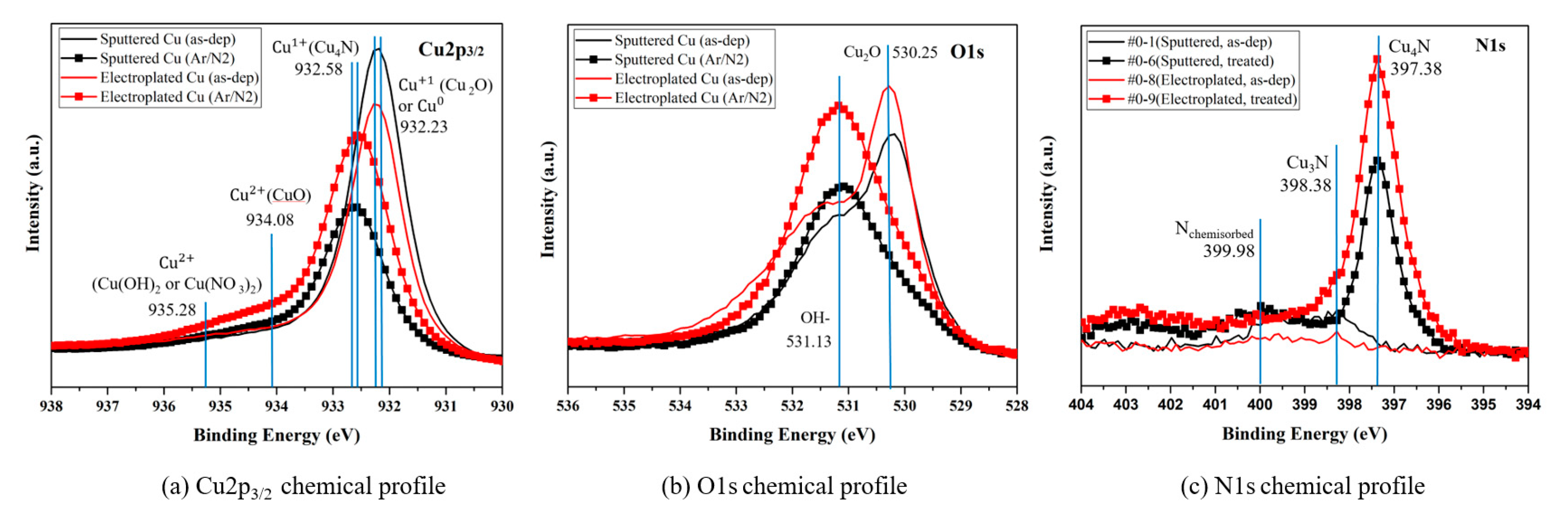
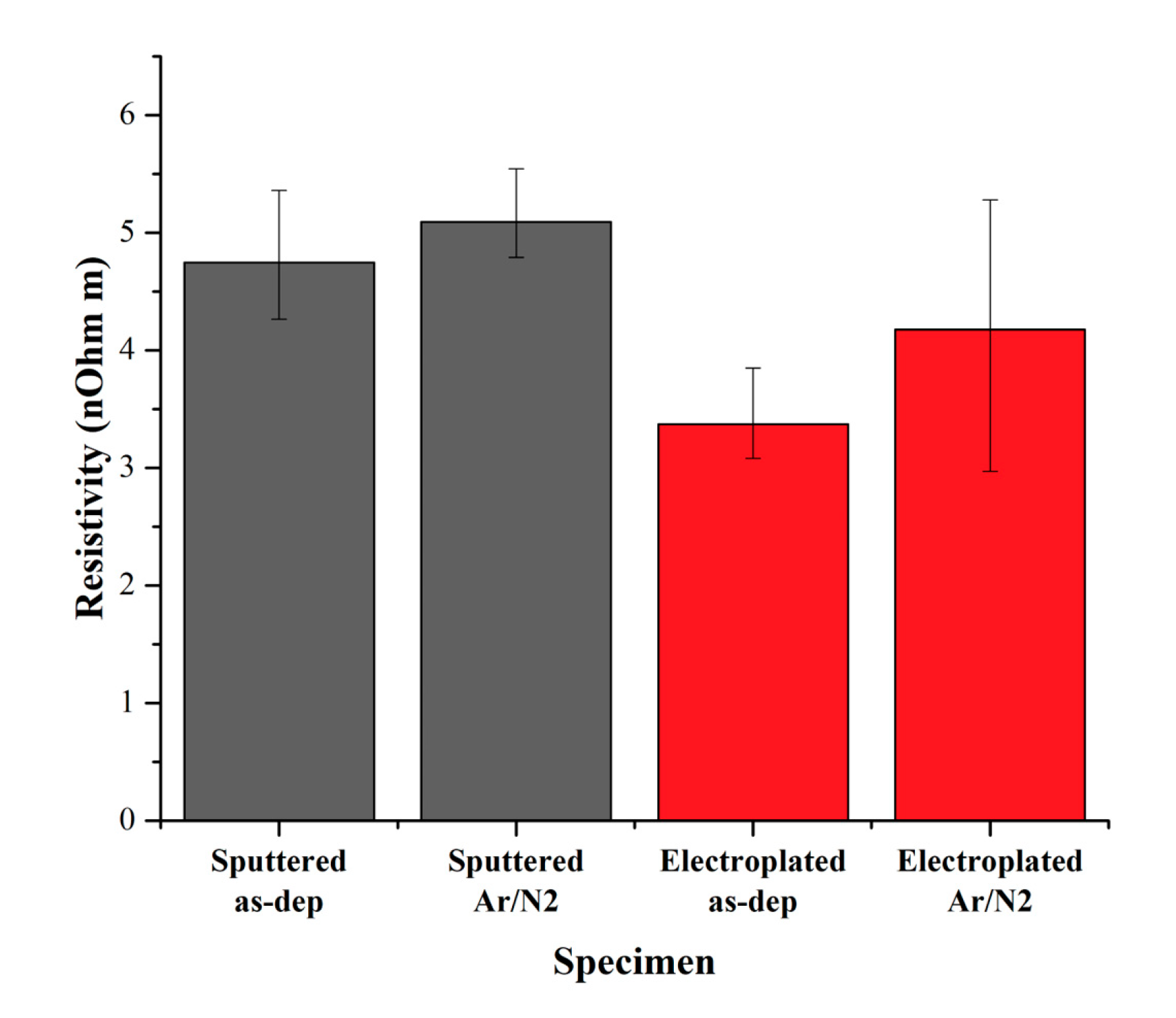
3. Results and Discussion

Figure 3 shows the X-ray diffraction patterns of the sputtered and electroplated Cu thin films. All samples had the preferred orientation of Cu (111) plane, and the reduction of Cu (111) peak was more noticeable in the sputtered Cu thin films after the two-step plasma treatment. Almost no copper oxide or copper nitride peaks were observed in the XRD (X-ray diffraction) analysis due to the extremely thin oxide or nitride formation on the top surface of Cu thin films. Cu grain size was estimated using the Scherrer equation (grain size = Kλ/βcosθ where K is a shape facto, λ is the X-ray wavelength, β is the line broadening at half the maximum intensity, and θ is the Bragg angle.), and the sputtered Cu thin film showed slightly larger grain size than the electroplated Cu thin film, and the grain size increased about 10 nm after the two-step plasma treatment. This agreed with the TEM (transmission electron microscopy) results shown in Figure 4. The SEM images in Figure 4a showed a larger grain in the sputtered Cu thin film, and the diffraction patterns in Figure 4b showed small grains in random orientation since the diffraction resulted in circles instead of set of sharp dots. Both Cu thin films showed (111) planes, but the electroplated Cu thin film exhibited more defects such as dislocations and stacking faults than the sputtered Cu thin films as shown in Figure 4c.
Further studies on the chemical states of copper, oxygen, and nitrogen were undertaken using the XPS (X-ray photoelectron spectroscopy) analysis shown in Figure 5. For the as-deposited sample, the Cu2p peak of the sputtered Cu and electroplated Cu in Figure 5a occurred at 932.18 eV and 932.28.7 eV, respectively. The peak at 932.2 eV may be linked to a pure metallic copper (Cuo) or the Cu1+ chemical state of Cu2O [18,19,20], but it is most likely related to Cu2O because the O1s peak at ~530.2 eV in Figure 5b indicates Cu2O state. After the two-step plasma treatment, it was found that the Cu2O peak at 932.2 eV had almost disappeared, and the CuO peak appeared at 934.08 eV in Figure 5a. In addition, the Cu2p binding energy of the sputtered Cu moved toward a slightly higher binding energy at around 932.58 eV than the electroplated Cu. In Figure 5b the O1s peak at ~530.2 eV had also disappeared, and the only strong OH-related peak at 531.2 eV appeared. The N1s peak observed at 397.38 eV in Figure 5c, and the Cu2p peak at 932.58 eV in Figure 5a, which is a higher binding energy than the chemical state of Cu0 and the Cu1+ of Cu2O, led to the formation of Cu4N at the surface. The qualitative analysis of nitride formation using Cu2p XPS survey data is summarized in Table 2. It is clearly showed that the sputtered Cu showed little more Cu4N formation than the electroplated Cu. This seems to be because the electroplated Cu thin film may have more copper oxide on the surface than the sputtered Cu thin film initially due to the electroplating process characteristics and has a high surface roughness (Rq) due to small grains. In Figure 6, the measured surface roughness by AFM confirmed that the sputtered Cu had a much lower roughness value than the electroplated Cu, as expected from the TEM results. After the two-step plasma treatment, the surface roughness decreased in both the sputtered and electroplated Cu surfaces. The XPS analysis strongly implies that the two-step plasma treatment sufficiently removed copper oxide on Cu surface and formed copper nitride to prevent further oxidation.
In order to confirm the resistivity changes by the plasma treatment, the sheet resistance was measured to estimate the Cu resistivity, and the results are shown in Figure 7. The resistivity of sputter Cu was higher than electroplated Cu due to a larger grain size. The very small increase in resistivity was observed in the sputtered Cu after the two-step plasma treatment, whereas the higher increase in resistivity was observed in the electroplated Cu. It has been reported that Cu4N tends to offer metallic behavior and Cu3N for semiconducting behavior, unlike copper oxides [21]. This means that the electroplated Cu has more oxide or less nitride formation than the sputtered Cu.
Following the two-step plasma treatment, the two plasma-treated Cu wafers were bonded at 300 °C, and then the bonding quality at the bonded Cu interface was evaluated using SAT (scanning acoustic tomography) and FIB (focused ion beam) analysis. In general, the darker the spot color in the SAT images, the better the bonding quality at the Cu bonding interface. In a previous report [17], the black spot in the sputtered Cu showed a complete bonded Cu interface with full Cu diffusion. In Figure 8, the as-deposited sample showed extremely poor bonding quality, but after the two-step plasma treatment, the bonding quality significantly improved in the sputtered Cu, and somewhat improved in the electroplated Cu with incomplete spot-bonded images. Considering that neither warpage control nor surface planarization by CMP (chemical mechanical polishing) was performed, the sputtered Cu exhibited a better bonded Cu interface than the electroplated Cu. In the XPS and AFM analysis, the sputtered Cu was observed to form more copper nitride and less copper oxide on the Cu surface and had lower surface roughness than the electroplated Cu. This may explain better bonding quality in the sputtered Cu. Despite the inherent problem of blanket Cu wafer bonding process in this experiment, the two-step plasma treatment has shown the possibility of preventing continuous copper oxidation and allowing low-temperature Cu bonding.

4. Conclusions

In this study, the effect of two-step plasma treatment on sputtered and electroplated Cu surfaces was comparatively evaluated. The two-step plasma treatment using Ar and N2 gases was carried out on 200-mm Cu deposited wafers, and then a wafer pair was bonded at 300 °C in a vacuum. The sputtered Cu formed more copper nitride and less copper oxide and had lower surface roughness than the electroplated Cu. And the improved bonding quality of Cu bonded interface was more evident in sputtered Cu samples than in electroplated Cu samples. Overall, compared with the as-deposited sample, the two-stage plasma treated sample showed a passivated copper nitrate layer, improving the binding quality of the Cu bonded interface.

Author Contributions

Conceptualization, S.E.K.; Methodology, H.S., H.P.; Validation, H.S., H.P. and S.E.K.; Formal analysis, H.S., H.P.; Investigation, H.S.; Data curation, H.S., S.E.K.; Writing—original draft preparation, H.S., S.E.K.; Writing—review and editing, S.E.K.; Visualization, H.S.; Supervision, S.E.K.; Funding acquisition, S.E.K.

Funding

This research was supported by the MOTIE (Ministry of Trade, Industry & Energy (#20003524) and KSRC (Korea Semiconductor Research Consortium) support program for the development of the future semiconductor device and also was partially supported by Basic Science Research Program through the National Research Foundation of Korea (NSF) funded by the Ministry of Science and ICT (NRF-2018R1A2B6003921).

Conflicts of Interest

The authors declare no conflict of interest.

References

  1. List, R.S.; Webb, C.; Kim, S.E. 3D wafer stacking technology. In Proceedings of the Advanced Metallization Conference, San Diego, CA, USA, 1–3 October 2002. [Google Scholar]
  2. Das, S.; Chandrakasan, A.P.; Reif, R. Calibration of Rent’s rule models for three-dimensional integrated circuits. IEEE Trans. Very Large Scale Integr. Syst. 2004, 12, 359–366. [Google Scholar] [CrossRef]
  3. Morrow, P.; Kobrinsky, M.J.; Ramanathan, S.; Park, C.M.; Harmes, M.; Ramachandrarao, V.; Park, H.M.; Kloster, G.; List, S.; Kim, S.E. Wafer-level 3D interconnects via Cu bonding. In Proceedings of the Advanced Metallization Conference, San Diego, CA, USA, 19–21 October 2004. [Google Scholar]
  4. Kim, T.H.; Howlader, M.M.R.; Itoh, T.; Suga, T. Room temperature Cu–Cu direct bonding using surface activated bonding method. J. Vac. Sci. Technol. A 2003, 21, 449–453. [Google Scholar] [CrossRef]
  5. Tan, C.S.; Lim, D.F.; Ang, X.F.; Wei, J.; Leong, K.C. Low temperature Cu-Cu thermo-compression bonding with temporary passivation of self-assembled monolayer and its bond strength enhancement. Microelectron. Reliab. 2012, 52, 321–324. [Google Scholar] [CrossRef]
  6. Huffman, A.; Lannon, J.; Lueck, M.; Gregory, C.; Temple, D. Fabrication and characterization of metal-to-metal interconnect structures for 3-D integration. J. Instrum. 2009, 4, P03006. [Google Scholar] [CrossRef]
  7. Fan, J.; Lim, D.F.; Tan, C.S. Effects of surface treatment on the bonding quality of wafer-level Cu-to-Cu thermo-compression bonding for 3D integration. J. Micromech. Microeng. 2013, 23, 045025. [Google Scholar] [CrossRef]
  8. Huang, Y.-P.; Chien, Y.-S.; Tzeng, R.-N.; Chen, K.-N. Demonstration and electrical performance of Cu–Cu bonding at 150 °C with Pd passivation. IEEE Trans. Electron Devices 2015, 62, 2587–2592. [Google Scholar] [CrossRef]
  9. Panigrahy, A.K.; Ghosh, T.; Vanjari, S.R.K.; Singh, S.G. Demonstration of sub 150 °C Cu-Cu thermocompression bonding for 3D IC applications, utilizing an ultra-thin layer of manganin alloy as an effective surface passivation layer. Mater. Lett. 2017, 194, 86–89. [Google Scholar] [CrossRef]
  10. Liu, Z.; Cai, J.; Wang, Q.; Liu, L.; Zou, G. Modified pulse laser deposition of Ag nanostructure as intermediate for low temperature Cu-Cu bonding. Appl. Surf. Sci. 2018, 445, 16–23. [Google Scholar] [CrossRef]
  11. Kuwae, H.; Yamada, K.; Momose, W.; Shoji, S.; Mizuno, J. Cu-Cu Quasi-Direct Bonding with Atomically Thin-Au and Pt Intermediate Layer Using Atomic Layer Deposition. In Proceedings of the International Conference on Electronic Packaging, Niigata, Japan, 17–19 April 2019. [Google Scholar]
  12. Juang, J.-Y.; Lu, C.-L.; Chen, K.-J.; Chen, C.-C.A.; Hsu, P.-N.; Chen, C.; Tu, K.N. Copper-to-copper direct bonding on highly (111)-oriented nanotwinned copper in no-vacuum ambient. Sci. Rep. 2018, 8, 13910. [Google Scholar] [CrossRef] [PubMed]
  13. Enquist, P.; Fountain, G.; Petteway, C.; Hollingsworth, A.; Grady, H. Low cost of ownership scalable copper direct bond interconnect 3D IC technology for three dimensional integrated circuit applications. In Proceedings of the IEEE International Conference on 3D System Integration, San Francisco, CA, USA, 28–30 September 2009. [Google Scholar]
  14. Huyghebaert, C.; Van Olmen, J.; Civale, Y.; Phommahaxay, A.; Jourdain, A.; Sood, S.; Farrens, S.; Soussan, P. Cu to Cu interconnect using 3D-TSV and Wafer to Wafer thermocompression bonding. In Proceedings of the IEEE International Interconnect Technology Conference, Burlingame, CA, USA, 6–9 June 2010. [Google Scholar]
  15. Wang, D.Y.; Nakamine, N.; Hayashi, Y. Properties of various sputter-deposited Cu–N thin films. J. Vac. Sci. Technol. A 1998, 16, 2084–2092. [Google Scholar] [CrossRef]
  16. Du, Y.; Ji, A.L.; Ma, L.B.; Wang, Y.; Cao, Z.X. Electrical conductivity and photo reflectance of nanocrystalline copper nitride thin films deposited at low temperature. J. Cryst. Growth 2005, 280, 490–494. [Google Scholar] [CrossRef]
  17. Park, H.; Kim, S.E. Two-step plasma treatment on copper surface for low temperature Cu thermo-compression bonding. IEEE Trans. Compon. Packag. Manuf. Technol. 2019. [Google Scholar] [CrossRef]
  18. Navío, C.; Capitán, M.J.; Álvarez, J.; Yndurain, F.; Miranda, R. Intrinsic surface band bending in Cu3N (100) ultrathin films. Phys. Rev. B 2007, 76, 085105. [Google Scholar] [CrossRef]
  19. Okada, M.; Vattuone, L.; Moritani, K.; Savio, L.; Teraoka, Y.; Kasai, T.; Rocca, M. X-ray photoemission study of the temperature-dependent CuO formation on Cu(410) using an energetic O2 molecular beam. Phys. Rev. B 2007, 75, 233413. [Google Scholar] [CrossRef]
  20. Biesinger, M.C. Advanced analysis of copper X-ray photoelectron spectra. Surf. Interface Anal. 2017, 49, 1325–1334. [Google Scholar] [CrossRef]
  21. Gonzalez-Arrabal, R.; Gordillo, N.; Martin-Gonzalez, M.; Ruiz-Bustos, R.; Agulló-López, F. Thermal stability of copper nitride thin films: The role of nitrogen migration. J. Appl. Phys. 2010, 107, 103513. [Google Scholar] [CrossRef] [Green Version]
Figure 1. Fabrication process flow.
Applsci 09 03535 g001
Figure 2. Bonding process profile.
Applsci 09 03535 g002
Figure 3. XRD analysis of sputtered and electroplated Cu thin films.
Applsci 09 03535 g003
Figure 4. TEM analysis of plasma treated Cu thin films: (a) cross-sectional images, (b) diffraction pattern indexing, (c) lattice indexing.
Applsci 09 03535 g004
Figure 5. XPS analysis: (a) Cu2p, (b) O1s, (c) N1s.
Applsci 09 03535 g005
Figure 6. Roughness of plasma treated Cu thin films measured by atomic force microscopy (AFM).
Applsci 09 03535 g006
Figure 7. Estimated resistivity of plasma treated Cu thin films by measuring sheet resistance.
Applsci 09 03535 g007
Figure 8. Bonded interface by SAT and FIB measurements.
Applsci 09 03535 g008
Table 1. Process condition for sputtered and electroplated Cu samples.
SubstrateCu DepositionAr Plasma ConditionN2 Plasma Condition
Sputtered
Cu sample
Si/SiO2(700 nm)/
Ti(50 nm)
Flow rate Ar 80sccm,
RF 2500 W,
Pressure 5mTorr
Flow rate 150sccm,
RF 100 W,
Pressure 7.5mTorr,
Time 30 s
Flow rate 45sccm,
RF 200 W,
Pressure 7.5mTorr
Time 300 s
Electroplated
Cu sample
Si/SiO2(700 nm)/
Ti(50 nm)/Cu(100 nm)
Current density 2ASD
Freq. 40 Hz,
Speed 40 rpm
Table 2. Qualitative analysis of nitride formation using Cu2p XPS data.
Cu4N/CuCuO/Cu
Sputtered Cu sample0.8420.070
Electroplated Cu sample0.7410.095

