All-Sputtering, High-Transparency, Good-Stability Coplanar Top-Gate Thin Film Transistors

 , ,
, ,  , and
, and 
Abstract
:1. Introduction
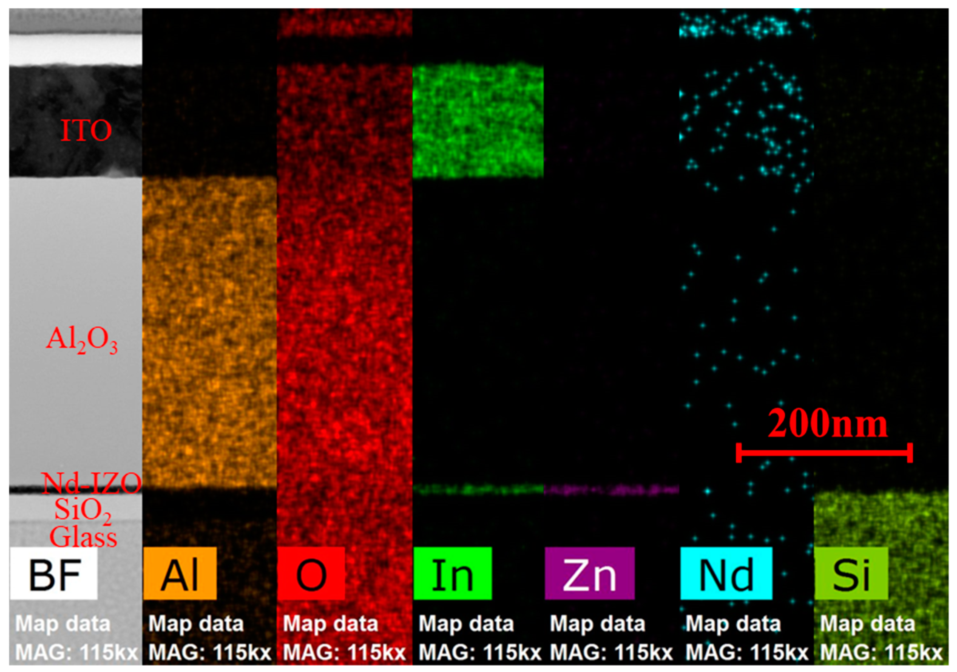
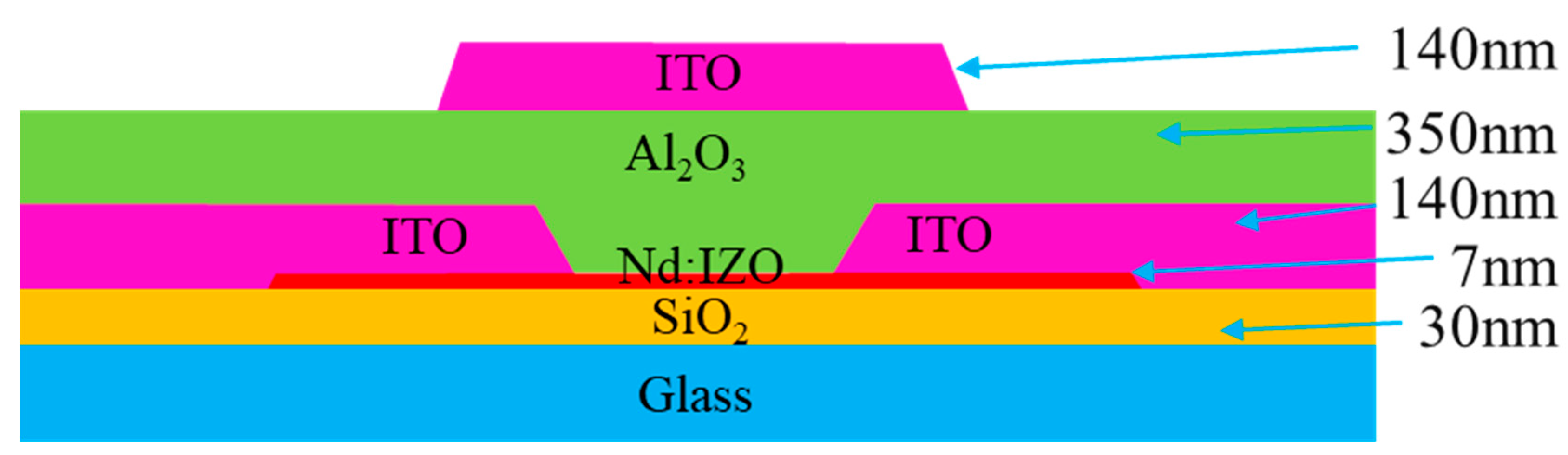
2. Experimental
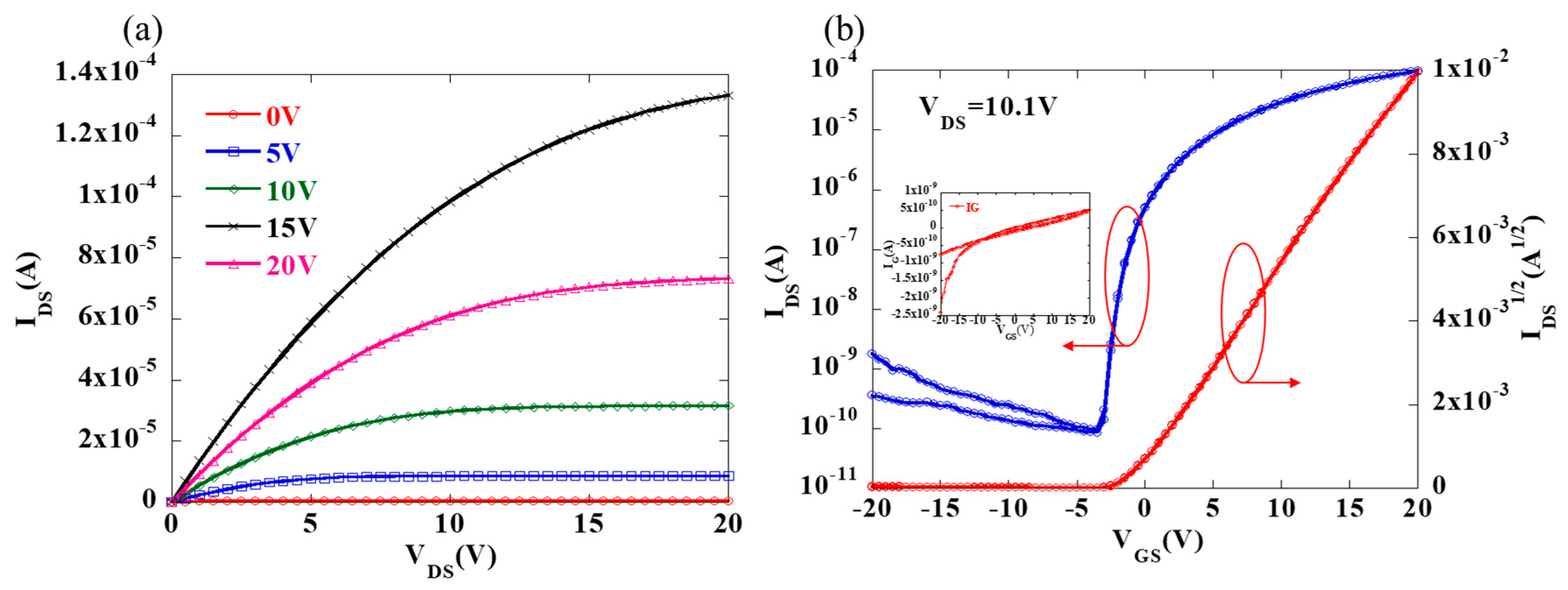
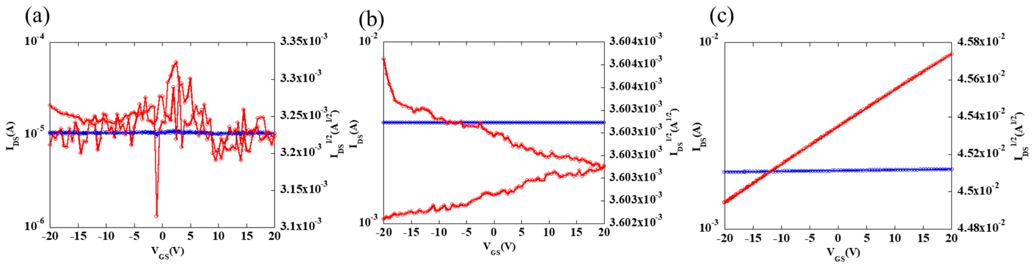
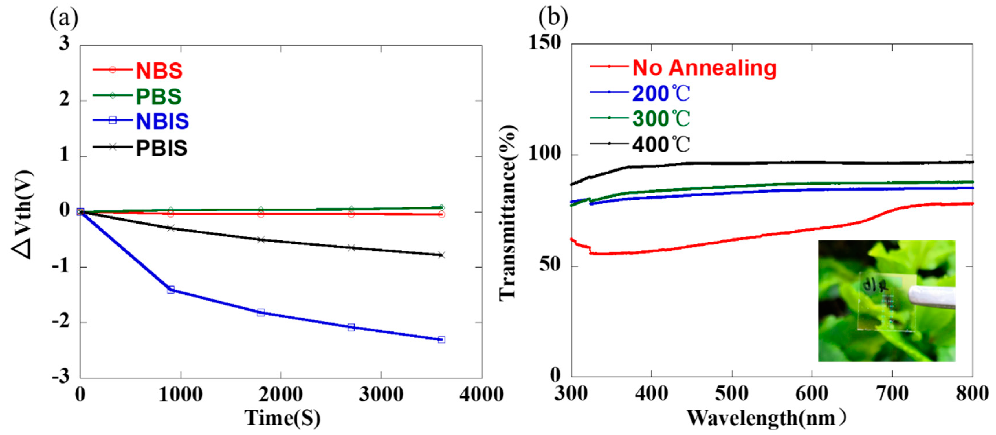
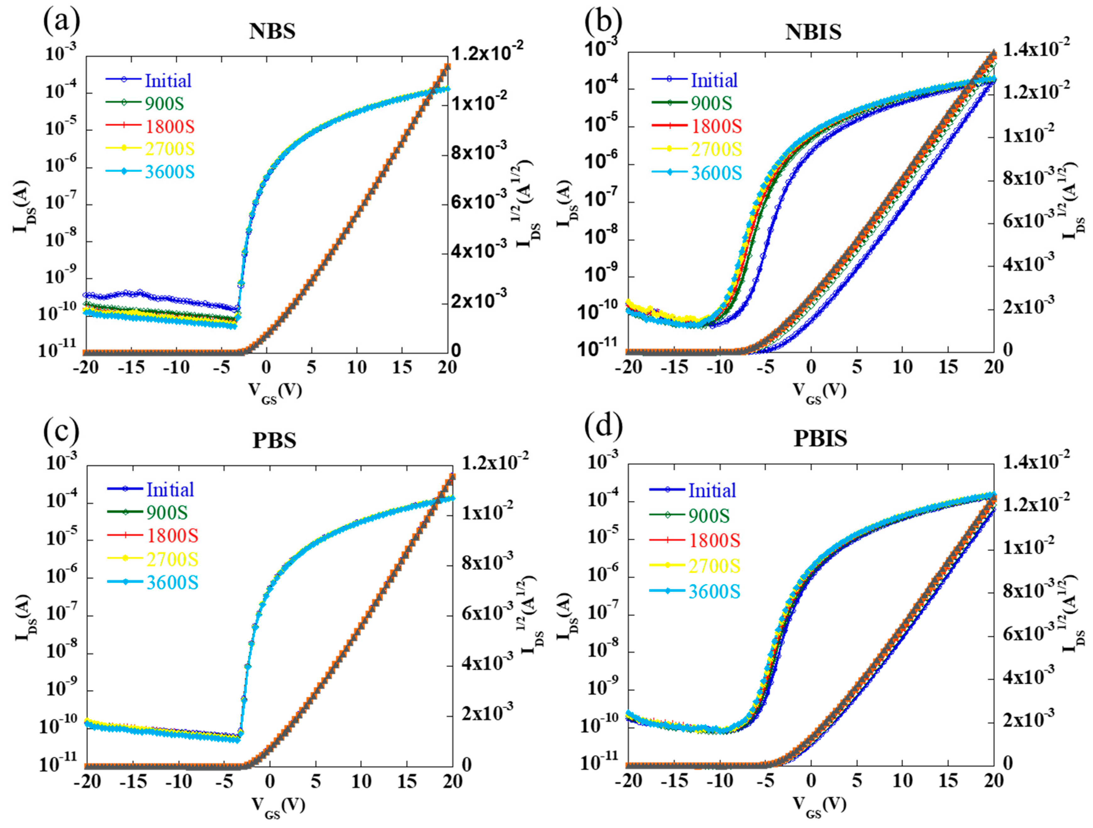
3. Results and Discussion
4. Conclusions
Author Contributions
Funding
Acknowledgments
Conflicts of Interest
References
- Yu, X.; Marks, T.J.; Facchetti, A. Metal Oxides for Optoelectronic Applications. Nat. Mater. 2016, 15, 383–396. [Google Scholar] [CrossRef] [PubMed]
- Lee, S.; Nathan, A. Subthreshold Schottky-barrier Thin-Film Transistors with Ultralow Power and High Intrinsic Gain. Science 2016, 354, 302–304. [Google Scholar] [CrossRef] [PubMed]
- Lee, H.N.; Kyung, J.; Sung, M.C.; Kim, D.Y.; Sun, K.K.; Kim, S.J.; Chang, N.K.; Kim, H.G.; Kim, S.T. Oxide TFT with Multilayer Gate Insulator for Backplane of AMOLED Device. J. Soc. Inf. Disp. 2012, 16, 265–272. [Google Scholar] [CrossRef]
- Conley, J.F. Instabilities in Amorphous Oxide Semiconductor Thin-Film Transistors. IEEE Trans. Device Mater. Reliab. 2010, 10, 460–475. [Google Scholar] [CrossRef]
- Jung, H.; Kim, W.; Park, B.; Woo, W.J.; Oh, I.; Lee, S.J.; Kim, Y.C.; Myoung, J.; Gatineau, S.; Dussarrat, C.; et al. Enhanced Light Stability of InGaZnO Thin-Film Transistors by Atomic-Layer-Deposited Y2O3 with Ozone. ACS Appl. Mater. Interfaces 2018, 10, 2143–2150. [Google Scholar] [CrossRef] [PubMed]
- Hu, S.; Lu, K.; Ning, H.; Zheng, Z.; Zhang, H.; Fang, Z.; Yao, R.; Xu, M.; Wang, L.; Lan, L.; et al. High Mobility Amorphous Indium-Gallium-Zinc-Oxide Thin-Film Transistor by Aluminum Oxide Passivation Layer. IEEE Electron Device Lett. 2017, 38, 879–882. [Google Scholar] [CrossRef]
- Song, Y.; Xu, R.; He, J.; Siontas, S.; Zaslavsky, A.; Paine, D.C. Top-Gated Indium–Zinc–Oxide Thin-Film Transistors within Situ Al2O3/HfO2 Gate Oxide. IEEE Electron Device Lett. 2014, 35, 1251–1253. [Google Scholar] [CrossRef]
- Hsieh, H.; Wu, C.; Chien, C.; Chen, C.; Yang, C.; Wu, C. Influence of Channel-Deposition Conditions and Gate Insulators On Performance and Stability of Top-Gate IGZO Transparent Thin-Film Transistors. J. Soc. Inform. Display 2010, 18, 796. [Google Scholar] [CrossRef]
- Lee, J.; Cho, I.; Lee, J.; Cheong, W.; Hwang, C.; Kwon, H. Comparative Study of Electrical Instabilities in Top-Gate InGaZnO Thin Film Transistors with Al2O3 and Al2O3/SiNx Gate Dielectrics. Appl. Phys. Lett. 2009, 94, 222112. [Google Scholar] [CrossRef]
- Lin, C.; Chien, C.; Wu, C.; Hsieh, H.; Wu, C.; Yeh, Y.; Cheng, C.; Lai, C.; Yu, M. Top-Gate Staggered a-IGZO TFTs Adopting the Bilayer Gate Insulator for Driving AMOLED. IEEE Trans. Electron Devices 2012, 59, 1701–1708. [Google Scholar] [CrossRef]
- Fakhri, M.; Theisen, M.; Behrendt, A.; Görrn, P.; Riedl, T. Top-Gate Zinc Tin Oxide Thin-Film Transistors with High Bias and Environmental Stress Stability. Appl. Phys. Lett. 2014, 104, 251603. [Google Scholar] [CrossRef]
- Lu, K.; Yao, R.; Hu, S.; Liu, X.; Wei, J.; Wu, W.; Ning, H.; Xu, M.; Lan, L.; Peng, J. High-Performance and Flexible Neodymium- Doped Oxide Semiconductor Thin-Film Transistors with Copper Alloy Bottom-Gate Electrode. IEEE Electron Device Lett. 2018, 39, 839–842. [Google Scholar] [CrossRef]
- Park, J.; Kim, S.; Kim, C.; Kim, S.; Song, I.; Yin, H.; Kim, K.K.; Lee, S.; Hong, K.; Lee, J. High-Performance Amorphous Gallium Indium Zinc Oxide Thin-Film Transistors through N2O Plasma Passivation. Appl. Phys. Lett. 2008, 93, 733. [Google Scholar] [CrossRef]
- Lee, J.; Park, J.S.; Pyo, Y.S.; Dong, B.L.; Kim, E.H.; Stryakhilev, D.; Kim, T.W.; Jin, D.U.; Mo, Y.G. The Influence of the Gate Dielectrics on Threshold Voltage Instability in Amorphous Indium-Gallium-Zinc Oxide Thin Film Transistors. Appl. Phys. Lett. 2009, 95, 043509. [Google Scholar] [CrossRef]
- Kim, D.; Fu, Y.; Kim, S.; Lee, W.; Lee, K.H.; Chung, H.K.; Lee, H.J.; Yang, H.; Chae, H. Polyethyleneimine Ethoxylated-Mediated All-Solution-Processed High-Performance Flexible Inverted Quantum Dot-Light-Emitting Device. ACS Nano 2017, 11, 1982. [Google Scholar] [CrossRef] [PubMed]
- Lin, Z.; Lan, L.; Xiao, P.; Sun, S.; Li, Y.; Song, W.; Gao, P.; Peng, J. Studies on Ndx In1−XO3 Semiconducting Thin Films Prepared by Rf Magnetron Sputtering. Appl. Phys. Lett. 2014, 105, 142104. [Google Scholar] [CrossRef]
- Song, E.; Lan, L.; Xiao, P.; Lin, Z.; Sun, S.; Li, Y.; Song, W.; Gao, P.; Peng, J. Thin-Film Transistors with Neodymium-Incorporated Indium–Zinc-Oxide Semiconductors. IEEE Trans. Electron Devices 2016, 63, 1916–1920. [Google Scholar] [CrossRef]
- Park, J.S.; Maeng, W.; Kim, H.; Park, J. Review of Recent Developments in Amorphous Oxide Semiconductor Thin-Film Transistor Devices. Thin Solid Films 2012, 520, 1679–1693. [Google Scholar] [CrossRef]
- Son, K.S.; Park, J.S.; Kim, T.S.; Kim, H.S.; Seo, S.J.; Kim, S.J.; Seon, J.B.; Ji, K.H.; Jeong, J.K.; Ryu, M.K. Improvement of Photo-Induced Negative Bias Stability of Oxide Thin Film Transistors by Reducing the Density of Sub-Gap States Related to Oxygen Vacancies. Appl. Phys. Lett. 2013, 102, 710. [Google Scholar] [CrossRef]
- Chowdhury, M.D.H.; Um, J.G.; Jin, J. Remarkable Changes in Interface O Vacancy and Metal-Oxide Bonds in Amorphous Indium-Gallium-Zinc-Oxide Thin-Film Transistors by Long Time Annealing at 250 °C. Appl. Phys. Lett. 2014, 105, 2945. [Google Scholar] [CrossRef]
- Yang, B.S.; Park, S.; Oh, S.; Kim, Y.J.; Jeong, J.K.; Hwang, C.S.; Kim, H.J. Improvement of the Photo-Bias Stability of the Zn–Sn–O Field Effect Transistors by an Ozone Treatment. J. Mater. Chem. 2012, 22, 10994–10998. [Google Scholar] [CrossRef]
- Cho, B.; Lee, J.; Seo, H.; Jeon, H. Electrical Stability Enhancement of the Amorphous In-Ga-Zn-O Thin Film Transistor by Formation of Au Nanoparticles On the Back-Channel Surface. Appl. Phys. Lett. 2013, 102, 488. [Google Scholar] [CrossRef]
- Pei, Y.U.; Lin, L.; Zheng, W.; Qu, Y.; Huang, Z.; Lai, F. Effect of Passing Electric Current on the Electrical and Optical Properties of Ito Films in Air. Surf. Rev. Lett. 2009, 16, 887–893. [Google Scholar] [CrossRef]


| Layer | Pressure (mTorr) | Power (W) | O2/Ar ratio (%) | Time (s) | Thickness (nm) |
|---|---|---|---|---|---|
| SiO2 | 1 | 100 | 0 | 900 | 30 |
| Nd-IZO | 5 | 80 | 5 | 300 | 7 |
| ITO | 5 | 100 | 0 | 600 | 140 |
| Al2O3 | 1 | 120 | 0 | 12600 | 350 |
| ITO | 5 | 100 | 0 | 600 | 140 |
| Time (s) | Vth (V) NBS | Vth (V) NBIS | Vth(V) PBS | Vth (V) PBIS |
|---|---|---|---|---|
| Initial | −0.03 | −1.81 | −0.06 | −0.52 |
| 900 | −0.06 | −3.21 | −0.03 | −0.81 |
| 1800 | −0.06 | −3.62 | −0.03 | −1.02 |
| 2700 | −0.07 | −3.88 | −0.02 | −1.17 |
| 3600 | −0.07 | −4.11 | −0.01 | −1.30 |
© 2018 by the authors. Licensee MDPI, Basel, Switzerland. This article is an open access article distributed under the terms and conditions of the Creative Commons Attribution (CC BY) license (http://creativecommons.org/licenses/by/4.0/).
Share and Cite
Chen, J.; Huang, X.; Li, Q.; Fang, Z.; Ning, H.; Tao, R.; Liang, H.; Zhou, Y.; Yao, R.; Peng, J. All-Sputtering, High-Transparency, Good-Stability Coplanar Top-Gate Thin Film Transistors. Appl. Sci. 2019, 9, 83. https://doi.org/10.3390/app9010083
Chen J, Huang X, Li Q, Fang Z, Ning H, Tao R, Liang H, Zhou Y, Yao R, Peng J. All-Sputtering, High-Transparency, Good-Stability Coplanar Top-Gate Thin Film Transistors. Applied Sciences. 2019; 9(1):83. https://doi.org/10.3390/app9010083
Chicago/Turabian StyleChen, Jianqiu, Xiuqi Huang, Qunjie Li, Zhiqiang Fang, Honglong Ning, Ruiqiang Tao, Hongfu Liang, Yicong Zhou, Rihui Yao, and Junbiao Peng. 2019. "All-Sputtering, High-Transparency, Good-Stability Coplanar Top-Gate Thin Film Transistors" Applied Sciences 9, no. 1: 83. https://doi.org/10.3390/app9010083
APA StyleChen, J., Huang, X., Li, Q., Fang, Z., Ning, H., Tao, R., Liang, H., Zhou, Y., Yao, R., & Peng, J. (2019). All-Sputtering, High-Transparency, Good-Stability Coplanar Top-Gate Thin Film Transistors. Applied Sciences, 9(1), 83. https://doi.org/10.3390/app9010083