Article

Evolution of Transient Liquid-Phase Sintered Cu–Sn Skeleton Microstructure During Thermal Aging

1
Manufacturing Engineering Center, Mitsubishi Electric Corporation, Hyogo 6618661, Japan
2
Division of Materials and Manufacturing Science, Graduate School of Engineering, Osaka University, Osaka 5650871, Japan
*
Author to whom correspondence should be addressed.
Appl. Sci. 2019, 9(1), 157; https://doi.org/10.3390/app9010157
Submission received: 19 December 2018 / Accepted: 27 December 2018 / Published: 4 January 2019
(This article belongs to the Special Issue Selected Papers from the NMJ2018)

Abstract

:
The evolution of the transient liquid-phase sintered (TLPS) Cu–Sn skeleton microstructure during thermal aging was evaluated to clarify the thermal reliability for die-attach applications. The Cu–Sn skeleton microstructure, which consists of Cu particles connected with Cu–Sn intermetallic compounds partially filled with polyimide resin, was obtained by the pressure-less TLP sintering process at 250 °C for 1 min using a novel Cu-solder-resin composite as a bonding material in a nitrogen atmosphere. Experimental results indicate that the TLPS joints were mainly composed of Cu, Cu6Sn5, and Cu3Sn in the as-bonded state, where submicron voids were observed at the interface between Cu3Sn and Cu particles. After thermal aging at 150, 175, and 200 °C for 1000 h, the Cu6Sn5 phase fully transformed into Cu3Sn except at the chip-side interface, where the number of the submicron voids appeared to increase. The averaged shear strengths were found to be 22.1 (reference), 22.8 (+3%), 24.0 (+9%), and 19.0 MPa (−14%) for the as-bonded state and specimens aged at 150, 175, and 200 °C for 1000 h, respectively. The TLPS joints maintained a shear strength over 19 MPa after thermal aging at 200 °C for 1000 h because of both the positive and negative impacts of the thermal aging, which include the transformation of Cu6Sn5 into Cu3Sn and the formation of submicron voids at the interface, respectively. These results indicate an excellent thermal reliability of the TLPS Cu–Sn skeleton microstructure.

1. Introduction

The demand for high heat endurance bonding solutions is rising steadily because of next generation power modules with wide bandgap semiconductor materials such as silicon carbide (SiC) [1,2]. There is a strong need for power modules to operate at high powers and frequencies with a high integration and miniaturization capability. Moreover, the SiC chips have lower power losses and higher switching speeds, even at elevated temperatures. These applications provide higher operation temperatures, which have recently exceeded 175 °C or reached 200 °C compared to the conventional 150 °C. The bonding layers are exposed to high temperature operation atmospheres. Therefore, high heat tolerance bonding technologies as alternatives to conventional Sn-based solders are in high demand. Sinter bonding using nano- or micro-particles is one of the most promising technologies and has been reported to provide outstanding thermal and electrical conductivity and reliable performance [3,4,5,6]. However, the sinter bonding technology requires complicated industrial equipment and processing because of the necessity of the pressure-assisted bonding process, so it cannot be widely applicable to industrial use. Another high-heat-tolerance bonding solution is strongly required for these reasons.
In recent years, transient liquid-phase (TLP) bonding has been developed as a promising packaging technique for next generation power modules [7,8,9,10]. Low melting point materials (Sn, In) and high melting point materials (Cu, Ag, Ni) are provided as layers or mixed powders that isothermally solidify during processing, which have higher re-melting points than the employed bonding materials. The technique involving the mixed powders as the bonding material is called transient liquid-phase sintering [11,12,13]. In a Cu–Sn system, the bonding layer is composed of Cu6Sn5 and Cu3Sn intermetallic compounds (IMCs), whose melting points are 415 °C and 640 °C, respectively. The mechanical properties of the Cu–Sn IMCs indicate higher strengths and creep resistances compared to conventional Sn-based solders [14]. These properties indicate that the Cu–Sn transient liquid-phase sintered (TLPS) joints could be appropriate as a temperature resistant method for power electronics applications; however, Cu–Sn IMCs have been generally used for the purposes of crack formation in conventional soldering because of their quite brittle and stiff properties [15,16,17]. These mechanical properties of the IMCs cause joint fracture during thermal stresses despite the higher melting point of the TLP joints [18,19,20]. The authors proposed a novel approach for reducing the stiffness of TLPS joints by controlling the microstructural morphology using a Cu-solder-resin composite as the bonding material [21,22], where a skeleton shaped microstructure consisting of Cu particles connected with Cu–Sn IMC bridges partially filled with polyimide resin was observed. In addition, the Cu–Sn skeleton microstructure showed a superior thermal cyclic reliability to a conventional Sn-based solder owing to the stiffness reduction effects of the joints. However, the precise study of the microstructural evolution of the joints during high-temperature operation has not yet been investigated.
In the present study, the evolution of the TLPS Cu–Sn skeleton microstructure during thermal aging was evaluated by shear strength tests, X-ray diffraction analysis, microstructure observation, and a fractographical approach. From these results, the microstructural and mechanical evolutions of the TLPS Cu–Sn skeleton joints are discussed.

2. Experimental Procedure

The Cu-solder-resin composite investigated in this work is a paste that mainly contains Cu particles, Sn–3Ag–0.5Cu (SAC305) solder particles, and polyimide-type thermosetting resin, as shown in Figure 1. The melting point of the solder is 220 °C. The cure temperature of the polyimide resin is 230–240 °C. The sizes of the Cu particles and solder particles are approximately 10 and 3 μm, respectively. The content of the copper in wt.% is approximately three times higher than that of the solder, which is designed to consume the solder through the formation of Cu–Sn IMCs. The content of the polyimide resin is approximately 20% in volume within the total of the Cu, solder, and polyimide resin. The polyimide resin is chosen by a curing temperature close to the melting point of the solder and by the soft mechanical properties, whose yield strength is approximately 1 MPa, which was expected to easily deform while embedded within the microstructure of the Cu and IMCs.
Figure 2 shows a schematic of the die-attached specimen in this work. Properties were obtained from the joints between the Kovar (Ni–Co–Fe alloy) chips and the directly bonded copper substrates, composed of two 0.3-mm-thick copper electrodes bonded to a 0.6-mm-thick silicon nitride (Si3N4) substrate. The chips had dimensions of 7 × 7 × 2 mm and a Ni/Au surface metallization. The thickness of the Ni and Au metallization was 2.0 and 0.1 μm, respectively. Before bonding, the chips were mounted onto the composite paste, which was printed on the substrate with a 100-μm thickness in advance. After preheating at 100 °C for 60 min in air using a hotplate, the specimens were bonded at 250 °C for 1 min in nitrogen atmosphere using a reflow furnace (VSU28, Invacu, Ltd., Burgas, Bulgaria). No pressure was applied in this heating process. Afterward, the die-attached specimens were subjected to thermal aging testing at 150, 175, and 200 °C for 500 or 1000 h in air. Analyses of the cross-sections and fracture surfaces of the aged specimens were performed by field emission scanning electron microscopy (FE-SEM; SU8000, Hitachi High-Technologies Corporation, Tokyo, Japan) and energy dispersive X-ray spectrometry (EDX; EMAX Evolution, HORIBA, Ltd., Kyoto, Japan). The crystal structure of each phase in the TLPS layer was identified by X-ray diffraction (XRD; D8 DISCOVER, Bruker Corporation, Billerica, MA, USA) apparatus, as shown in Figure 3. The specimens for XRD were prepared by a tilted cross-sectioning method for resin-molded specimens. The die-attached specimens were subjected to shear tests with a cross head speed of 100 μm/s at room temperature by a bond tester (CONDOR 150, XYZTEC). The average value of the two samples was regarded as the shear strength. After the shear test, the fracture surfaces were analyzed using FE-SEM and EDX.

3. Results

Figure 4 presents XRD results of the Cu-solder-resin composite paste and a bonding layer in the as-bonded state. Sn, Ag3Sn, and Cu peaks are detected in the composite paste, while Cu6Sn5, Cu3Sn, Ag3Sn, and Cu peaks are detected in the as-bonded state. In the as-bonded state, the Sn peaks, which are detected in the composite paste, fully disappear, while the Cu6Sn5 and Cu3Sn peaks appear. The disappearance of Sn and appearance of Cu–Sn IMCs could have occurred through isothermal solidification reactions between the Cu particles and solder particles during bonding. A cross-sectional SEM image of the as-bonded TLPS joint is shown in Figure 5, which indicates that the dark gray Cu particles are connected with the light gray bridges of the Cu–Sn IMCs within a black polyimide resin matrix. This shows the unique microstructure of the TLPS joint, which is a Cu-IMC skeleton shaped microstructure partially filled with polyimide resin. Figure 6a shows the magnified structures of the chip side interface. (Cu,Ni)6Sn5 is observed on the Ni/Au metalized chip surface, and no intermediate layers are detected between them. An intermediate layer composed of Cu3Sn IMCs is observed between the Cu particles and (Cu,Ni)6Sn5 IMCs. Figure 6b shows the substrate side interface, where Cu6Sn5 IMCs are observed on the Cu electrode of the substrate with an intermediate layer of Cu3Sn IMCs. These phases were confirmed by EDX results, as shown in Table 1. In addition, it should be noted that submicron voids are observed in the Cu3Sn layer, as shown in Figure 6. The submicron voids are observed in the Cu3Sn layer on the Cu particles but not on the Cu substrate.
Cross-sectional SEM images of the TLPS joints aged at 150, 175, and 200 °C for 1000 h, which are shown in Figure 7, show little change compared to the as-bonded state, as shown in Figure 5. The XRD results of the TLPS bonding layer aged at 150, 175, and 200 °C for 1000 h, as shown in Figure 8, show that Cu, Ag3Sn, and Cu3Sn peaks—and no Cu6Sn5 peaks—are detected in the aged state. This indicates that the Cu6Sn5, which are detected only in the as-bonded state, fully transformed into the Cu3Sn phase during the thermal aging for 1000 h. Focusing on the interfacial microstructure on the chip side (Figure 9 and Table 2) surface and substrate side (Figure 10 and Table 3) surface, both the Cu3Sn phase and residual (Cu,Ni)6Sn5 phase are observed at the chip side interface, whereas only the Cu3Sn phase is observed at the substrate side interface. Although a small amount of the (Cu,Ni)6Sn5 phase could remain because of the Ni dissolution from the chip metallization, it can be concluded from these XRD and EDX results that the highest amount of the Cu6Sn5 phase, as seen in the as-bonded state, transforms into Cu3Sn through the thermal aging. In addition, it should be noted that the number of submicron voids at the interface between the Cu3Sn and Cu particles apparently increases through the thermal aging, as can be seen from a comparison between Figure 6 (as-bonded) and Figure 9 and Figure 10 (aged).
Figure 11 illustrates the relationship between the shear strengths of the TLPS joints and aging conditions. The shear strength of the as-bonded joints is approximately 22.1 MPa. During the aging process, the shear strengths aged at 150 and 175 °C increase from 22.1 to 24.4 and 27.4 MPa in the first 500 h, respectively; afterward, they decrease to 22.8 and 24.0 MPa, respectively, after 1000 h. In contrast, that aged at 200 °C remains constant in the first 500 h and slightly decreases afterward to 19.0 MPa after 1000 h. The lowest shear strength of all the aged specimens is approximately 19 MPa, which is quite high when compared to the requirement of MIL-STD-883, Method 2019.7 (>0.5 MPa, 7 × 7 mm in die-size). This indicates that the joints could be applied to high-temperature applications with an excellent shear strength stability. The representative fracture surfaces of the as-bonded and aged specimens are shown in Figure 12. The fractography of the as-bonded specimen shows a brittle fracture surface on the Cu6Sn5, as shown in Figure 12a,b. The fractography of the aged specimens also shows a brittle surface. However, a fracture clearly appears at the interface between Cu and Cu3Sn, as shown in Figure 12c–h. The morphology of the fractured surface appears similar to a “boiled egg” and “peeled eggshell”, which represents the Cu particle and Cu3Sn layer covering them. Such unique fracture surfaces are observed only on the aged specimens. Based on the results, the change in the fracture behavior could have occurred by the microstructural variation through thermal aging.

4. Discussion

Cu6Sn5 was not detected in the joints aged at 150–200 °C for 1000 h except at the chip side interface, as it was fully transformed to Cu3Sn. There are two possible reactions for the transformation from Cu6Sn5 to Cu3Sn, as shown in Equations (1) and (2):
9 Cu + Cu 6 Sn 5 5 Cu 3 Sn ,
Cu 6 Sn 5 2 Cu 3 Sn + 3 Sn .
The values of the Gibbs free energy changes of the two reactions calculated by Bao et al. [23] are approximately −89 and 10 kJ/mol (150–200 °C), respectively. Thus, the reaction in Equation (1) was the main pathway for the transformation from Cu6Sn5 to Cu3Sn under the aging conditions in this study. The transformation from Cu6Sn5 to Cu3Sn could affect the joint strengths because of the different mechanical properties of Cu6Sn5 and Cu3Sn. For example, numerical studies estimated the elastic moduli of Cu6Sn5 and Cu3Sn [24,25]. Some experimental studies evaluated Young’s modulus of Cu6Sn5 at the macro-scale [26,27] and micro-scale [28,29,30,31]. Furthermore, Liu et al. evaluated the mechanical properties of Cu3Sn and Cu6Sn5 through both experimental and modelling techniques of micro-cantilever bending tests of the IMCs [32]. Although there is a wide variability in the values of their mechanical properties, the Cu3Sn generally exhibits superior properties—including a high strength, high elongation, and low elastic modulus—compared to those of Cu6Sn5. For instance, Liu et al. reported the tensile strengths of Cu3Sn and Cu6Sn5 to be 2.15 and 1.13 GPa and the tensile strains of Cu3Sn and Cu6Sn5 to be 0.016 and 0.010, respectively [32]. In addition, Lee et al. reported the bonding strength of TLPS joints composed of Cu3Sn to be five times higher than that composed of Cu6Sn5 [10]. Based on these studies, the transformation from Cu6Sn5 to Cu3Sn could have a positive effect on improving the joint strengths through thermal aging.
Despite the fact that the transformation from Cu6Sn5 to Cu3Sn might have improved the mechanical properties of the joints, the shear strengths of the TLPS joints showed little increase (150 and 175 °C) or a slight decrease (200 °C) through thermal aging in this study, as shown in Figure 11 in Section 3. The submicron voids observed in the Cu3Sn, as shown in the SEM images (i.e., Figure 9 and Figure 10 in Section 3), could adversely affect the TLPS joint strengths. Interestingly, the submicron voids were observed in the Cu3Sn layer on the Cu particles, but not on the Cu substrate, as shown in Figure 6, Figure 9 and Figure 10 in Section 3. Some studies demonstrated that submicron voids could be formed because of Kirkendall voids within the TLP layers of Cu–Sn [23,33,34], Ni–Sn [35], and Ag–Sn [23] systems. The Kirkendall voids were also observed in joints consisting of Sn-based solders and Cu [15,36,37,38]. Yu et al. reported that the formation of Kirkendall voids as the diffusion rate of Cu atoms is much higher than that of Sn atoms in the Cu3Sn layer between the Cu substrate and SAC305 solder [36]. However, previous results on Kirkendall void formation in Cu/Sn systems are not always consistent because of impurity atoms in the joints. Yu et al. [36] demonstrated that S segregation to a Cu/Cu3Sn interface localized Kirkendall voids at the interface. Laurilla et al. [37] suggested that impurity atoms (not identified) in an electroplated Cu film assisted void formation. Moreover, Yang et al. [38] suggested that excess H in a Cu pad introduced during electroplating condensed into voids in Cu3Sn. Although further studies are necessary, the submicron voids observed in the Cu3Sn phase only on the Cu particles in this study might have occurred because of impurity atoms in the Cu particles. Based on the observation results of the cross-section before/after thermal aging, the increase in the amount of the submicron voids could negatively affect the TLPS joint strengths.
The microstructural evolution aged at 150–200 °C can be approximately described as the following evolving model, as shown in Figure 13. First, the original metallurgical microstructure of the TLPS layer was mainly composed of Cu6Sn5 (or (Cu,Ni)6Sn5 at the chip side interface), residual Cu particles, and Cu3Sn layers in between the Cu6Sn5 and Cu particles, as shown in Figure 13a. Submicron voids formed at the interface between the Cu3Sn and Cu particles due to the possible mechanisms of the Kirkendall void. Secondly, with the increase in aging time, the transformation of the Cu6Sn5 (or (Cu,Ni)6Sn5 at the chip side interface) into Cu3Sn through the diffusion of Cu atoms from the residual Cu particles and the formation of submicron voids at the interface between the Cu3Sn and residual Cu particles occurred simultaneously, as shown in Figure 13b. Finally, with the increase in the aging time, the residual Cu6Sn5, except for the small amount of (Cu,Ni)6Sn5 at the chip side interface, fully transformed into Cu3Sn. In addition, the number of submicron voids gradually increased, as shown in Figure 13c. The analysis of the thermal aging characteristics for the TLP sintering shows that the joints aged at 150–200 °C for 1000 h maintained a shear strength exceeding 19 MPa on average, as shown in Figure 11 in Section 3, because of both the positive and negative impacts of thermal aging on the shear strengths, which include the transformation of Cu6Sn5 into Cu3Sn and the formation of submicron voids at the interface between the Cu3Sn and residual Cu particles, respectively. In other words, the TLPS layer could produce relatively stable strengths for die-attach applications through metallurgical reactions during thermal aging.

5. Conclusions

This study investigated the microstructural evolution and change in mechanical properties of the TLPS Cu–Sn skeleton microstructure using a Cu-solder-resin composite during thermal aging at 150–200 °C, and the mechanism of phase transformation and void formation was discussed. The following conclusions can be made:
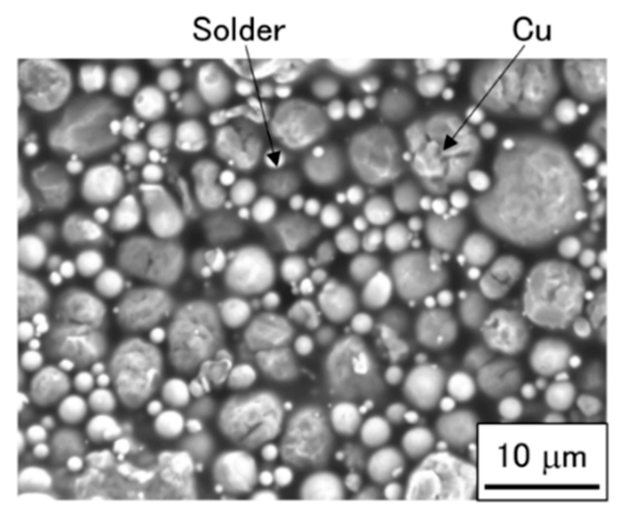
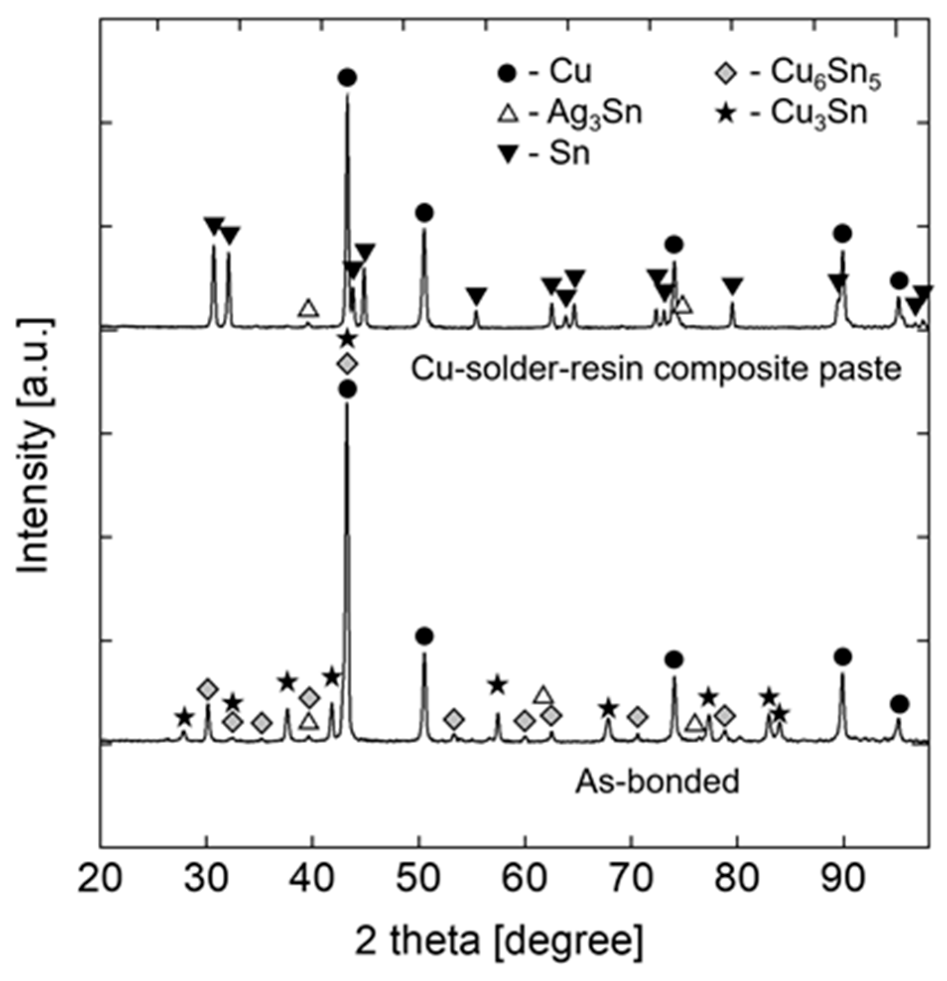
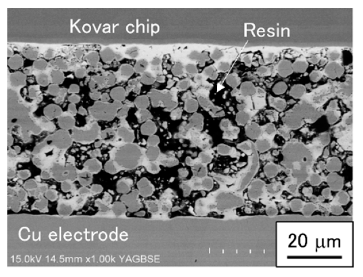
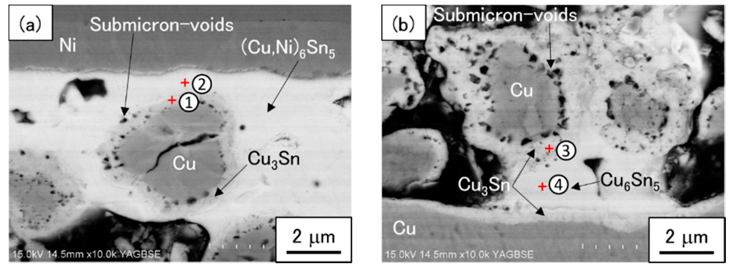
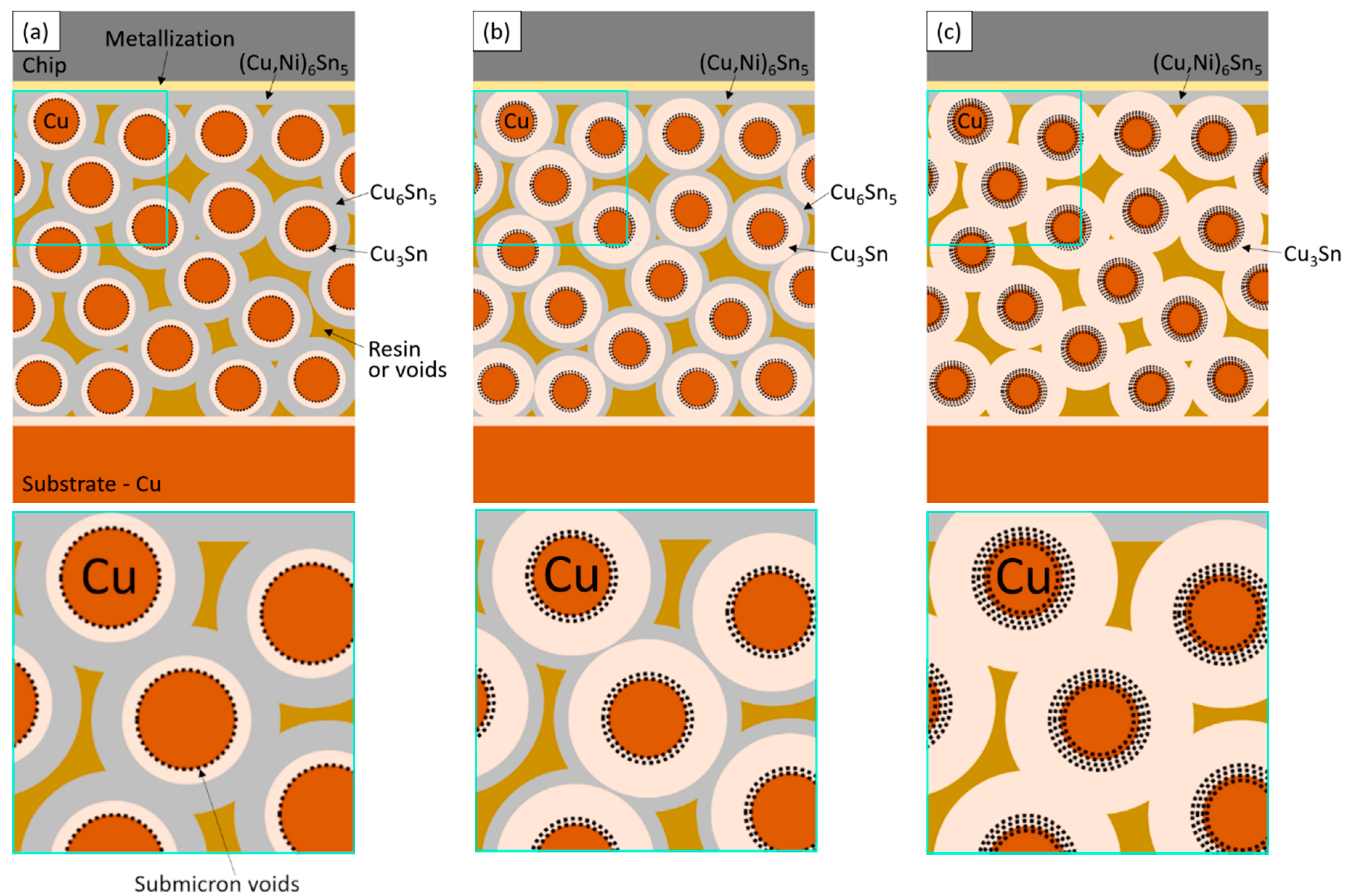
  • In the as-bonded state, the Cu–Sn skeleton microstructure was identified as comprising Cu particles connected with Cu6Sn5 and Cu3Sn IMCs partially filled with polyimide resin. In addition, submicron voids were observed at the interface between the Cu3Sn phase and Cu particles.
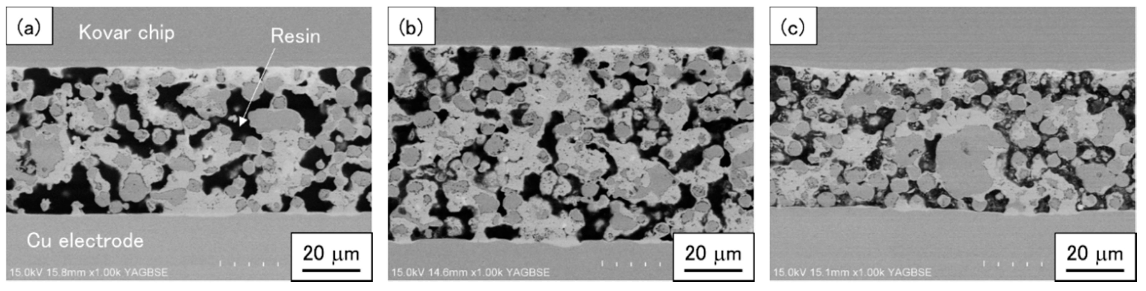
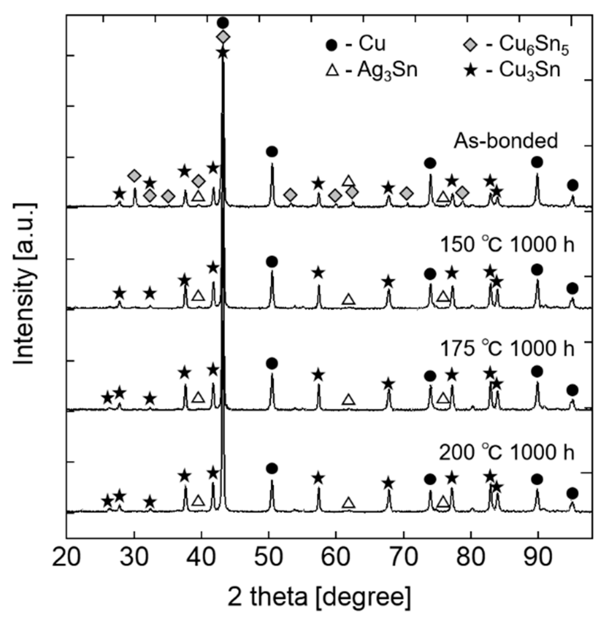
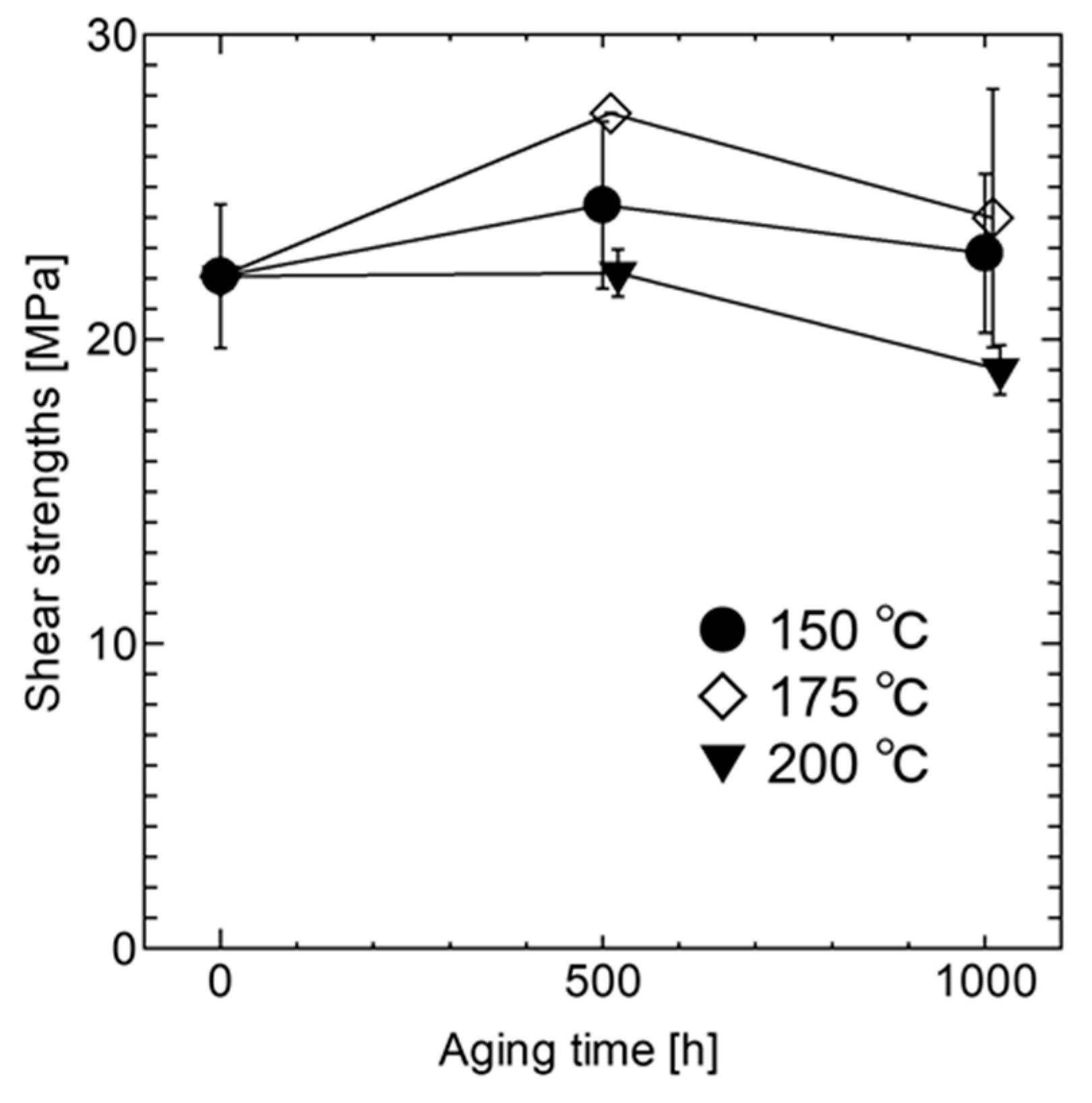
  • After aging at 150–200 °C for 1000 h, the Cu6Sn5 phase fully transformed into Cu3Sn except for the small amount of (Cu,Ni)6Sn5 phase at the chip side interface. The phase transformation from Cu6Sn5 into Cu3Sn could have a positive impact on the shear strengths owing to the better mechanical properties of the Cu3Sn. Furthermore, the number of submicron voids at the interface between Cu3Sn and Cu particles appeared to increase after aging, which should be because of the Kirkendall effects between them. The formation of submicron voids could have a negative impact on the shear strengths, suggesting a good agreement with the factography after aging.
  • The averaged shear strengths were found to be 22.1 (reference), 22.8 (+3%), 24.0 (+9%), and 19.0 MPa (−14%) for the as-bonded state and the specimens aged at 150, 175, and 200 °C for 1000 h, respectively. The TLPS joints maintained a shear strength over 19 MPa after the thermal aging at 200 °C for 1000 h because of both the positive and negative impacts of the thermal aging, as mentioned above. These results indicate an excellent thermal reliability of the TLPS Cu–Sn skeleton microstructure.

Author Contributions

Conceptualization, H.T., Y.K. and A.H.; Investigation, H.T.; Methodology, H.T., A.L., T.M. and T.S.; Project administration, H.Y.; Resources. H.T. and H.Y.; Supervision, Y.K. and A.H.; Validation, H.T. and H.Y.; Visualization, H.T.; Writing—original draft, H.T.; Writing—review & editing; H.T., A.L., T.M., T.S., Y.K. and A.H.

Funding

This research received no external funding.

Conflicts of Interest

The authors declare no conflict of interest.

References

  1. McNutt, T.; Passmore, B.; Fraley, J.; McPherson, B.; Shaw, R.; Olejniczak, K.; Lostetter, A. High-Performance, Wide-Bandgap Power Electronics. J. Electron. Mater. 2014, 43, 4552–4559. [Google Scholar] [CrossRef]
  2. Drevin-Bazin, A.; Lacroix, F.; Barbot, J.F. SiC die attach for high-temperature applications. J. Electron. Mater. 2014, 43, 695–701. [Google Scholar] [CrossRef]
  3. Hirose, A.; Tatsumi, H.; Takeda, N.; Akada, Y.; Ogura, T.; Ide, E.; Morita, T. A novel metal-to-metal bonding process through in-situ formation of Ag nanoparticles using Ag2O microparticles. J. Phys. Conf. Ser. 2009, 165, 2074. [Google Scholar] [CrossRef]
  4. Tatsumi, H.; Kumada, S.; Fukuda, A.; Yamaguchi, H.; Kashiba, Y. Impact of Metallurgical and Mechanical Properties of Sintered Silver Nanoparticles on Die-attach Reliability of High-temperature Power Modules. J. Microelectron. Electron. Packag. 2016, 13, 121–127. [Google Scholar] [CrossRef]
  5. Alarifi, H.; Hu, A.; Yavuz, M.; Zhou, Y.N. Silver nanoparticle paste for low-temperature bonding of copper. J. Electron. Mater. 2011, 40, 1394–1402. [Google Scholar] [CrossRef]
  6. Peng, P.; Hu, A.; Gerlich, A.P.; Zou, G.; Liu, L.; Zhou, Y.N. Joining of Silver Nanomaterials at Low Temperatures: Processes, Properties, and Applications. ACS Appl. Mater. Interfaces 2015, 7, 12597–12618. [Google Scholar] [CrossRef]
  7. Mustain, H.A.; Brown, W.D.; Ang, S.S. Transient liquid phase die attach for high-temperature silicon carbide power devices. IEEE Trans. Compon. Packag. Technol. 2010, 33, 563–570. [Google Scholar] [CrossRef]
  8. Bajwa, A.A.; Qin, Y.; Reiner, R.; Quay, R.; Wilde, J. Assembly and Packaging Technologies for Higherature and High-Power GaN Devices. IEEE Trans. Compon. Packag. Manuf. Technol. 2015, 5, 1402–1416. [Google Scholar] [CrossRef]
  9. Yoon, S.W.; Glover, M.D.; Shiozaki, K. Nickel-tin transient liquid phase bonding toward high-temperature operational power electronics in electrified vehicles. IEEE Trans. Power Electron. 2013, 28, 2448–2456. [Google Scholar] [CrossRef]
  10. Lee, B.S.; Yoon, J.W. Cu-Sn Intermetallic Compound Joints for High-Temperature Power Electronics Applications. J. Electron. Mater. 2018, 47, 430–435. [Google Scholar] [CrossRef]
  11. Shearer, C.; Shearer, B.; Matijasevic, G.; Gandhi, P. Transient liquid phase sintering composites: Polymer adhesives with metallurgical bonds. J. Electron. Mater. 1999, 28, 1319–1326. [Google Scholar] [CrossRef]
  12. Feng, H.; Huang, J.; Yang, J.; Zhou, S.; Zhang, R.; Chen, S. A Transient Liquid Phase Sintering Bonding Process Using Nickel-Tin Mixed Powder for the New Generation of High-Temperature Power Devices. J. Electron. Mater. 2017, 46, 4152–4159. [Google Scholar] [CrossRef]
  13. Hu, T.; Chen, H.; Li, M.; Zhao, Z. Cu@Sn Core–Shell Structure Powder Preform for High-Temperature Applications Based on Transient Liquid Phase Bonding. IEEE Trans. Power Electron. 2016, 32, 441–451. [Google Scholar]
  14. Mu, D.; Huang, H.; McDonald, S.D.; Nogita, K. Creep and mechanical properties of Cu6Sn5 and (Cu,Ni)6Sn5 at elevated temperatures. J. Electron. Mater. 2013, 42, 304–311. [Google Scholar] [CrossRef]
  15. Li, C.; Hu, X.; Jiang, X.; Li, Y. Interfacial reaction and microstructure between the Sn3Ag0.5Cu solder and Cu–Co dual-phase substrate. Appl. Phys. A Mater. Sci. Process. 2018, 124, 484. [Google Scholar] [CrossRef]
  16. Takaku, Y.; Liu, X.J.; Ohnuma, I.; Kainuma, R.; Ishida, K. Interfacial Reaction and Morphology Between Molten Sn Base Solders and Cu Substrate. Mater. Trans. 2004, 45, 646–651. [Google Scholar] [CrossRef] [Green Version]
  17. Tu, P.L.; Chan, Y.C.; Lai, J.K.L. Effect of intermetallic compounds on the thermal fatigue of surface mount solder joints. IEEE Trans. Compon. Packag. Manuf. Technol. Part B 1997, 20, 87–93. [Google Scholar] [CrossRef]
  18. Dudek, R.; Sommer, P.; Fix, A.; Rzepka, S.; Michel, B. Reliability issues for high temperature interconnections based on transient liquid phase soldering. In Proceedings of the 2013 14th International Conference on Thermal, Mechanical and Multi-Physics Simulation and Experiments in Microelectronics and Microsystems (EuroSimE 2013), Wroclaw, Poland, 14–17 April 2013; pp. 1–8. [Google Scholar]
  19. Guth, K.; Oeschler, N.; Böwer, L.; Speckels, R.; Strotmann, G.; Heuck, N.; Krasel, S.; Ciliox, A. New assembly and interconnect technologies for power modules. In Proceedings of the 2012 7th International Conference on Integrated Power Electronics Systems (CIPS), Nuremberg, Germany, 6–8 March 2012; pp. 1–5. [Google Scholar]
  20. Guth, K.; Heuck, N.; Stahlhut, C.; Ciliox, A.; Oeschler, N.; Ag, I.T. End-of-life investigation on the XT interconnect technology. In Proceedings of the PCIM Europe 2015, Nuremberg, Germany, 19–20 May 2015; pp. 72–79. [Google Scholar]
  21. Tatsumi, H.; Lis, A.; Monodane, T.; Yamaguchi, H.; Kashiba, Y.; Hirose, A. Transient Liquid Phase Sintering Using Copper-Solder-Resin Composite for High- temperature Power Modules. In Proceedings of the 2018 IEEE 68th Electronic Components and Technology Conference (ECTC), San Diego, CA, USA, 29 May–1 June 2018; pp. 564–567. [Google Scholar]
  22. Tatsumi, H.; Lis, A.; Yamaguchi, H.; Kashiba, Y.; Hirose, A. Stiffness Reduction Approach of Transient Liquid-Phase Sintered Joints for SiC Die-Attach Applications. 2018; submitted. [Google Scholar]
  23. Bao, Y.; Wu, A.; Shao, H.; Zhao, Y.; Liu, L.; Zou, G. Microstructural evolution and mechanical reliability of transient liquid phase sintered joint during thermal aging. J. Mater. Sci. 2018, 54, 765–776. [Google Scholar] [CrossRef]
  24. Chen, W.H.; Yu, C.F.; Cheng, H.C.; Lu, S.T. Crystal size and direction dependence of the elastic properties of Cu3Sn through molecular dynamics simulation and nanoindentation testing. Microelectron. Reliab. 2012, 52, 1699–1710. [Google Scholar] [CrossRef]
  25. Shen, T.; Feng, Y.; Hu, C.; Dai, H.; Song, M.; Yang, W.; Liu, H.; Wei, X. First-principles calculations of structural and mechanical properties of Cu6Sn5. Optoelectron. Adv. Mater. Rapid Commun. 2016, 10, 268–272. [Google Scholar] [CrossRef]
  26. Subrahmanvan, B. Elastic Moduli of some complicated binary alloys systems. Mater. Trans. 1971, 13, 93–95. [Google Scholar]
  27. Rhee, H.; Lucas, J.P.; Subramanian, K.N. Micromechanical characterization of thermomechanically fatigued lead-free solder joints. J. Mater. Sci. Mater. Electron. 2002, 13, 477–484. [Google Scholar] [CrossRef]
  28. Che, F.X.; Pang, J.H.L. Characterization of IMC layer and its effect on thermomechanical fatigue life of Sn-3.8Ag-0.7Cu solder joints. J. Alloys Compd. 2012, 541, 6–13. [Google Scholar] [CrossRef]
  29. Deng, X.; Chawla, N.; Chawla, K.K.; Koopman, M. Deformation behavior of (Cu, Ag)-Sn intermetallics by nanoindentation. Acta Mater. 2004, 52, 4291–4303. [Google Scholar] [CrossRef]
  30. Xu, L.; Pang, J.H.L. Nanoindentation on SnAgCu lead-free solder joints and analysis. J. Electron. Mater. 2006, 35, 2107–2115. [Google Scholar] [CrossRef]
  31. Yang, P.-F.; Lai, Y.-S.; Jian, S.-R.; Chen, J.; Chen, R.-S. Nanoindentation identifications of mechanical properties of Cu6Sn5, Cu3Sn, and Ni3Sn4 intermetallic compounds derived by diffusion couples. Mater. Sci. Eng. A 2008, 485, 305–310. [Google Scholar] [CrossRef]
  32. Liu, L.; Chen, Z.; Liu, C.; Wu, Y.; An, B. Micro-mechanical and fracture characteristics of Cu6Sn5 and Cu3Sn intermetallic compounds under micro-cantilever bending. Intermetallics 2016, 76, 10–17. [Google Scholar] [CrossRef]
  33. Mo, L.; Chen, Z.; Wu, F.; Liu, C. Microstructural and mechanical analysis on Cu-Sn intermetallic micro-joints under isothermal condition. Intermetallics 2015, 66, 13–21. [Google Scholar] [CrossRef]
  34. Liu, X.; He, S.; Nishikawa, H. Low temperature solid-state bonding using Sn-coated Cu particles for high temperature die attach. J. Alloys Compd. 2017, 695, 2165–2172. [Google Scholar] [CrossRef]
  35. Feng, H.; Huang, J.; Peng, X.; Lv, Z.; Wang, Y.; Yang, J.; Chen, S.; Zhao, X. Microstructural Evolution of Ni-Sn Transient Liquid Phase Sintering Bond during High-Temperature Aging. J. Electron. Mater. 2018, 47, 4642–4652. [Google Scholar] [CrossRef]
  36. Yu, J.; Kim, J.Y. Effects of residual S on Kirkendall void formation at Cu/Sn-3.5Ag solder joints. Acta Mater. 2008, 56, 5514–5523. [Google Scholar] [CrossRef]
  37. Laurila, T.; Vuorinen, V.; Kivilahti, J.K. Interfacial reactions between lead-free solders and common base materials. Mater. Sci. Eng. R Rep. 2005, 49, 1–60. [Google Scholar] [CrossRef]
  38. Yang, W.; Messler, R.W.; Felton, L.E. Microstructure Evolution of Eutectic Sn-Ag Solder Joints.pdf. J. Electron. Mater. 1994, 23, 765–772. [Google Scholar] [CrossRef]
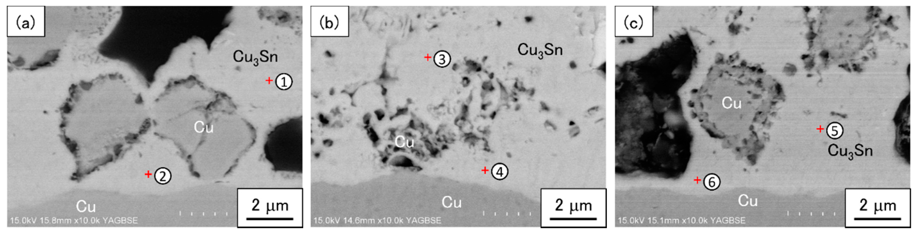
Figure 1. SEM image of Cu-solder-resin composite paste.
Applsci 09 00157 g001
Figure 2. Schematic of a die-attached specimen.
Applsci 09 00157 g002
Figure 3. XRD method using tilted cross-sectioning: (a) before cross-sectioning, (b) after cross-sectioning, (c) schematic of XRD arrangement, and (d) irradiated area of the transient liquid-phase sintered (TLPS) layer.
Applsci 09 00157 g003
Figure 4. XRD patterns of the Cu-solder-resin composite paste and the as-bonded TLPS bonding layer.
Applsci 09 00157 g004
Figure 5. Cross-sectional SEM image of an as-bonded TLPS joint.
Applsci 09 00157 g005
Figure 6. Cross-sectional SEM images of the interfaces between the bonding layer and (a) chip and (b) substrate, as-bonded.
Applsci 09 00157 g006
Figure 7. Cross-sectional SEM images of a TLPS joint aged at (a) 150, (b) 175, and (c) 200 °C for 1000 h.
Applsci 09 00157 g007
Figure 8. XRD patterns of the TLPS bonding layer as-bonded and aged at 150, 175, and 200 °C for 1000 h.
Applsci 09 00157 g008
Figure 9. Cross-sectional SEM images of the interfaces between the bonding layer and chip aged at (a) 150, (b) 175, and (c) 200 °C for 1000 h.
Applsci 09 00157 g009
Figure 10. Cross-sectional SEM images of the interfaces between the bonding layer and substrate aged at (a) 150, (b) 175, and (c) 200 °C for 1000 h.
Applsci 09 00157 g010
Figure 11. Shear strengths of TLPS joints aged at 150, 175, and 200 °C for 1000 h.
Applsci 09 00157 g011
Figure 12. Fracture surfaces of the joints (a,b) as-bonded and aged at (c,d) 150, (e,f) 175, and (g,h) 200 °C for 1000 h.
Applsci 09 00157 g012
Figure 13. Mechanism model of the microstructural evolution for the TLPS layer aged at 150–200 °C: (a) as-bonded, (b) gradual transformation of Cu6Sn5 into Cu3Sn and formation of submicron voids, and (c) fully-transformed structure with dominated Cu3Sn.
Applsci 09 00157 g013
Table 1. Chemical composition (at.%) in the marked areas in Figure 6 measured by EDX spectroscopy.
AreaCuSnNiAuPhase
173.825.0--1.2Cu3Sn
244.244.65.36.0(Cu,Ni)6Sn5 + Au
375.624.4----Cu3Sn
456.044.0----Cu6Sn5
Table 2. Chemical composition (at.%) in the marked areas in Figure 9 measured by EDX spectroscopy.
Aging ConditionAreaCuSnNiAuPhase
150 °C 1000 h174.224.7--1.0Cu3Sn
246.942.04.17.1(Cu,Ni)6Sn5 + Au
175 °C 1000 h372.826.0--1.2Cu3Sn
447.836.34.411.5(Cu,Ni)6Sn5 + Au
200 °C 1000 h571.726.6--1.7Cu3Sn
647.638.45.88.1(Cu,Ni)6Sn5 + Au
Table 3. Chemical composition (at.%) in the marked areas in Figure 10 measured by EDX spectroscopy.
Aging ConditionAreaCuSnNiAuPhase
150 °C 1000 h175.724.3----Cu3Sn
273.126.9----Cu3Sn
175 °C 1000 h373.626.4----Cu3Sn
478.721.3----Cu3Sn
200 °C 1000 h575.524.5----Cu3Sn
676.123.9----Cu3Sn

