1. Introduction
An electric arc represents a type of electrical discharge in gases that occurs when an electric current passes through a gas gap under the influence of an electric field. An electric arc used for welding, cutting, and surfacing of metals is referred to as a welding arc [
1,
2]. Owing to their characteristics, electrical discharges are suitable for generating high-performance plasma sources for various technological applications (plasma welding, surfacing, spraying, cutting, and melting of metals). As is known, arc discharges used in welding are characterized by the low value of the cathode fall of potential, which is close to the ionization energy of the atoms of a specific material. The small magnitude of the cathode fall of potential is a consequence of a high electron emission current from the cathode that arises at high total discharge currents of 1–10
5 A. Important technological characteristics of the arc include arc ignition and stability. This refers to the ability of the arc to maintain an unchanged spatial position relative to the electrodes in a stable burning mode, as well as its capability to deviate and move without extinction under the action of external and internal factors [
2]. A review of the literature shows that almost all studies evaluating the stability of welding arcs were focused on the assessment of current and voltage, electrode diameter, coating type, arc length, and the determination of their interrelations.
In [
3,
4], it was shown that the stability of arc ignition during TIG welding with direct current of reverse polarity in the range of low currents of 0.5–20 A depends on the cathode spots. It was shown that high speeds of movement of the cathode spot on the surface of the tungsten electrode at the initial stage of arc ignition with low current lead to arc extinguishing. The quality of mechanical treatment of the tungsten cathode affects the formation of the cathode spot and erosion of the tungsten electrode. Using a mechanically polished tungsten electrode, an arc of 0.7 A can be maintained. Reducing the radius of curvature at the tip of the tungsten electrode helps to reduce the time required to form a stable cathode spot.
It is worth noting that the widespread use of aluminum in various industries has raised the issue of aluminum welding [
5]. High-quality joints were only achieved using direct current (DC) with reverse polarity and alternating current (AC) [
6,
7,
8]. It has been established that cathode spots play an important role in aluminum welding. The formation of a weld pool during aluminum welding without the formation of an oxide film (Al
2O
3) depends on the cathode spot. The mechanisms of oxide film evaporation and the role of cathode spots in aluminum welding have been examined in detail in studies, and new hypotheses regarding film evaporation have been proposed [
6,
7,
8].
In the additive manufacturing of machine parts from aluminum using welding and plasma arcs, cathode spots play an important role in obtaining a high-quality product [
9,
10,
11].
At the same time, scientific works devoted to welding arcs have not addressed the physical nature of cathode and anode spots. Classic works on the physics of welding [
2] do not provide a comprehensive theory of cathode and anode spot formation. There are very few published works devoted to theoretical issues of cathode spot formation in welding arcs. Scientific works devoted to welding arcs do not address the physical nature of cathode and anode spots. Classic works on welding physics do not offer a comprehensive theory of cathode and anode spot formation. There are very few published works devoted to theoretical issues of cathode spot formation in a welding arc. There are no experimental studies devoted to the mechanisms of cathode spot formation in a welding arc for basic welding processes: Manual Metal Arc (MMA), TIG (Tungsten Inert Gas) TIG-DC, TIG-AC, MIG (Metal Inert Gas), MIGW (Metal Inert Gas Welding), MAG (Metal Active Gas), MAGW (Metal Active Gas Welding), FCAW (Flux Core Arc Welding), and SAW (Submerged Arc Welding).
At the same time, in the related field of vacuum arcs, extensive experimental and theoretical material has been accumulated [
12,
13,
14,
15,
16,
17,
18,
19,
20,
21,
22,
23,
24,
25,
26,
27,
28,
29,
30], which can be used as a first approach to evaluating the role of cathode and anode spots in the welding arc.
A commonly known classification of arc discharges is their division according to the nature of processes occurring on the cathode surface [
12,
13,
14,
15,
16,
17,
18,
19,
20]. In this case, two groups can be distinguished.
The first group corresponds to arc discharges with a hot cathode, whose average temperature is sufficient to provide a high thermionic emission current. This type of discharge may be either self-sustained or non-self-sustained, for example, when the cathode is externally heated.
The second group includes arc discharges with cathode spots. This type of discharge occurs when the average cathode temperature is insufficient to provide the thermionic emission current required to sustain the discharge. As a result, the discharge current density becomes localized in the cathode spots. The current density in the spots may reach extremely high values, up to 107 A/cm2, leading to local heating of the cathode material.
The physics of processes in cathode spots is highly complex and diverse, and therefore no generally accepted model exists to date [
12,
13,
14,
15]. Moreover, the physical nature of the aggregate state of matter within the spot, its shape, and its formation mechanism are still unknown. Even the question of why cathode material heating occurs during the formation of cathode spots remains a subject of discussion [
16,
19].
An analysis of numerous studies investigating cathode spots in the vacuum arc [
12,
13,
14,
15,
16,
17,
18,
19,
20,
21,
22,
23,
24,
25,
26,
27,
28,
29,
30,
31,
32,
33,
34] shows that the operating modes of arc discharges with cold cathodes differ according to the type of cathode spots observed. Cathode spots play a crucial role in closing the discharge current; they serve as the sources of the plasma-forming medium and electrons. At the same time, the key parameters are not only the commonly considered ones—arc current, external magnetic field strength, and cathode–anode distance—but also the cathode material (its thermophysical properties and chemical composition) and the structure of its surface [
12,
13,
14,
15].
For this reason, the spots reported in the literature often differ from one another in several properties. Even on the same material (copper), different researchers observed spots of various sizes carrying different currents.
For example, the authors of [
13], at a current of 200 A, observed only group cathode spots. The author of [
12], at currents of 3–10 A, observed spot cells but did not determine their dimensions. In works [
19,
20,
21,
22,
23], at currents of 50–70 A, spots with diameters ranging from 50 to 100 μm were observed; at currents of 10–15 A, diameters of 10–30 μm; and at currents below 10 A, diameters of 1–5 μm. In [
23], for copper cathodes at a current of 25–30 A, the spot diameter was 25–30 μm. In [
24,
25,
26], it was shown that the most probable crater diameter on copper cathodes increased with arc current.
Such differences in experimental values [
12,
13,
19,
20,
21,
22,
23,
24,
25,
26] obtained for the same material (copper) are determined by differences in arc burning modes (current, arc burning duration), as well as by the spatial and temporal resolution available to a particular researcher.
The author of work [
30] further complicated the classification of cathode spots by insisting on the fractal nature of the spot, by analogy with already known natural self-similar examples described in the extensive literature. The work [
30] itself contains no specific new information; it is merely descriptive in nature and summarizes already known experimental facts.
A more detailed attempt to apply fractal analysis was made by the authors of [
31], who applied the Minkowski–Bouligand method. According to the authors of [
31], determining the exact threshold value for the fractal dimension
D of the spot structure is difficult.
The topic of cathode spot theory has not been overlooked by artificial intelligence methods. For example, in [
32], an attempt was made to reveal the mechanism of cathode spot formation using neural networks. However, it should be noted that modern software tools employing artificial intelligence are mainly intended for statistical processing based on regression models. Prediction based on regression models is a statistical method that uses an equation to describe the relationship between a dependent variable (that which needs to be predicted) and one or more independent variables (influencing factors). The resulting equation makes it possible to perform predictions by estimating the value of the dependent variable for new values of the independent variables through interpolation (within the data range) or extrapolation (beyond the data range).
Despite the large number of experimental studies in the field of vacuum arcs [
12,
13,
14,
15,
16,
17,
18,
19,
20,
21,
22,
23,
24,
25,
26,
27,
28,
29,
30,
31,
32,
33,
34,
35,
36,
37,
38,
39,
40,
41,
42], we do not have dependent or independent variables suitable for modeling.
A review of the identified 24 publications shows that, in most studies, it is not specified which conditions (current, voltage, cathode diameter, pressure, etc.) are nominal and which constitute uncontrolled disturbances that deviate the actual operating conditions from the nominal ones, leading to deviations in the size and shape of the cathode spot from the predicted values.
As stated by the author of work [
33]: “He writes about the phenomenon of the cathode spot and asks questions that remain unanswered, despite the existence of a large body of work. In his work, he attempts to answer some of these questions from a phenomenological perspective, leaving the question of the spot’s structure unanswered.
All these questions require answers, but at present, we do not even have a reasonable, experimentally verifiable theory of cathode spot formation. This is due to the objective reasons associated with the phenomenon of cathode spots—the high temperature of the welding arc column (from 6000 to 30,000 °C), the currently unknown temperature of the cathode spots themselves (no direct and accurate measurements exist in the literature), the velocity of spot motion, their short lifetimes, and other factors. It is also due to the fact that there exist only two methods for experimental investigation: (1) the direct optical method using high-speed cameras [
13,
15,
19,
20,
21,
22,
23,
24,
27,
28,
29,
30], and (2) the indirect autograph method [
12,
27,
28,
29,
30], based on the examination of imprints left on the metal after the spots disappear.
Detailed analytical reviews of the experimental results obtained by these two methods are presented in [
13,
14,
15,
16,
30,
31,
32,
33,
34,
35,
36,
37,
38,
39,
40,
41,
42,
43], where the advantages and drawbacks of each method are considered. Several important facts should be noted.
Using the optical method, cathodes made of different materials with diameters up to 10 mm were studied, with discharge durations in the range of 1–103 μs at currents from 100 to 1000 A, as well as small-diameter cathodes of 200–500 μm with nanosecond resolution. In the analysis of optical images, primary attention was given to the velocity of spot motion, spot size, and lifetime.
In studies employing the autograph method, a wide range of crater and track sizes was observed (from 20 nm to 100 μm). The characteristics of craters (number, size distribution, and lifetime) depend on the type of cathode (film or bulk), arc current, arc duration, and observation time during arc burning.
A comparison of the accuracy of the two methods shows a substantial difference in the geometric dimensions of cathode spots—not by percentages, but by orders of magnitude—because the sizes of the optical images of the cathode spot do not correspond to the sizes of the imprints (autographs) observed on the cathode surface after the arc discharge.
The imperfection of both methods is related to the nature of the object being studied. In the optical measurement method, the captured frame contains the active zone of the cathode spot, which is characterized by strong electron emission and evaporation in the form of a plume of emitted and evaporated products. Therefore, in the optical method, what is studied is not the cathode spot itself and not its true size but the plasma cloud emitted by the spot. Emission photographs reflect the process of plasma expansion rather than the active spot zone where electrons are emitted, atoms evaporate, and plasma is formed [
19,
20,
21,
22,
23,
24,
25,
26,
27,
28,
29,
30,
31,
32,
33,
34,
35,
36,
37,
38,
39,
40,
41,
42,
43,
44,
45,
46,
47]. Emission photographs may exaggerate the apparent size of the spot.
The autograph method also has its limitations. For example, in [
47] it is noted that craters are not a direct image of the cathode spot. According to the author, the active spot region is characterized by strong electron emission and evaporation, which is always larger than the imprint left on the cathode surface. However, the author states this argument without supporting it with factual evidence.
In [
47], it was shown that the method of visualizing cathode spots, using the emission or absorption method, affects the interpretation of the geometric values of the cathode spot. Emission photographs from the linear radiation of the cathode spot indicate a larger spot size (about 100 μm) than the corresponding radius of the active spot, which is 10 μm, for discharges lasting from 10 ns to at least 100 μs. Cathode spots exist not only at the moment of ignition, but also throughout the entire discharge, and their location changes due to the movement of the spots. Absorption photographs show that spots of a size (10–20 μm) remain visible even 200 μs after ignition.
The authors of [
48] point out the important role of observation parameters, especially exposure time, since different researchers can find many values for observing cathode spots. They recommend that the exposure time should be set as short as possible, taking into account that a long exposure time can blur the image of a rapidly changing object undergoing rapid mixing and show only the general trajectory. A high-speed digital camera was used for three seconds (recording time) using several shutter speeds: 0.01 ms, 0.03 ms, from 0.05 ms to 0.25 ms and from 0.50 ms to 20 ms (maximum exposure time). It was found that the optimal exposure time should be from 0.03 ms to 0.10 ms, and the recommended observation time is 0.05 ms.
Using a high-speed camera (500,000 frames per second) to film cathode spots on the surface of an aluminum weld pool during the TIG-AC process allowed us to visualize two types of spots on the surface of the pool and beyond it [
49,
50]. It was traditionally believed that after the formation of the aluminum weld pool, the arc switches to a diffusion mode of combustion. However, studies have shown that rapidly moving cathode spots continue to exist on the surface of the aluminum pool.
At the same time, it should be noted that the cathode spot exerts not only thermal effects but also mechanical pressure on the metal surface due to the recoil pressure impulse of the cathode jet emitted from the spot. Any pressure must be spatially localized; it cannot be dimensionless in space and time. Therefore, the outer boundaries of the autograph correspond to the true size of the cathode spot, and the region of mechanical pressure either coincides with the outer boundaries of the autograph or is smaller [
12,
13,
44,
45,
51,
52].
Many authors have noted [
12,
13,
44,
45,
51,
52] that cathode spots leave autographs of thermo-deformation effects on the cathode surface, and these autographs most accurately reflect the geometric dimensions of cathode spots. In work [
44,
45], the results of experiments aimed at determining, by the autograph method [
12], the spatial shape and internal structure of cathode spots formed during the burning of the welding arc on film cathodes were presented. The hypothesis was proposed that cathode spots represent a concentrated heat source [
12,
13,
14,
15,
33,
34,
35,
36,
37,
38,
39,
40].
The author of [
44,
45] believes that part of the thermal energy, after evaporation of the film, must be transferred to the heating and melting of the substrate on which the film is deposited; as a result of such an action, a distinct thermal imprint of the welding arc cathode spot should remain on the substrate [
43,
44,
45].
To reveal its structure and substructure, it is important to select a substrate material with low thermal conductivity (to prevent blurring of the thermal imprint) and a relatively high melting/evaporation temperature (to increase the ablation threshold). Ordinary soda–lime glass satisfies these requirements, which made it possible to obtain clear autographs [
44,
45]. During the experimental verification of the hypothesis, it was found [
45] that the welding arc cathode spot consisted of individual cells that possessed a substructure in the form of separate current channels. Subsequently, the author proposed a new method for investigating cathode spots, combining the two methods (optical and autograph) into one by placing a high-speed camera on the reverse side of the cathode spot [
45]. In [
45], experimental dependencies were obtained for the average lifetime of the cathode spot for various film-cathode materials when observed from the reverse side. The number of cathode spots recorded from the reverse side as a function of exposure time was also determined experimentally [
45].
In our work [
43], results are presented on the visualization of cathode and anode spots in welding arcs, as well as results on the visualization of cathode spots from the reverse side. Developing the innovative ideas of the method proposed by Balanovskii, A.E., in [
45], conduct research regarding the existence of the reverse side of the cathode spot.
Analysis of experimental studies [
12,
13,
14,
15,
16,
19,
20,
21,
22,
23,
24,
25,
26,
27,
28,
29,
30,
31,
32,
33,
34,
35,
36] shows that the boundary of the cathode spot on the electrode surface is conditional, since along the surface there exists a continuous distribution of the parameters that determine the current-transfer process [
12,
13,
14,
15,
16,
46].
Because of the strong dependence of emission and plasma ionization on temperature, this boundary can be fairly well defined both in experiments and in theoretical calculations. Developing the idea of the author of [
45], one may assume that the cathode spot has a spatial shape in which the front and reverse sides of the spot exist. Thermal imprints of the cathode spot left on glass after the evaporation of the copper film [
12,
44] make it possible to record them through the glass from the reverse side [
43,
45].
The main objective of the present work is to improve the method of visualizing the reverse side of the cathode and anode spots in a welding arc and to carry out investigations of the size and structure of the spots.
2. Materials and Methods
From a methodological standpoint, the experimental procedures are described in detail in our works [
43,
44,
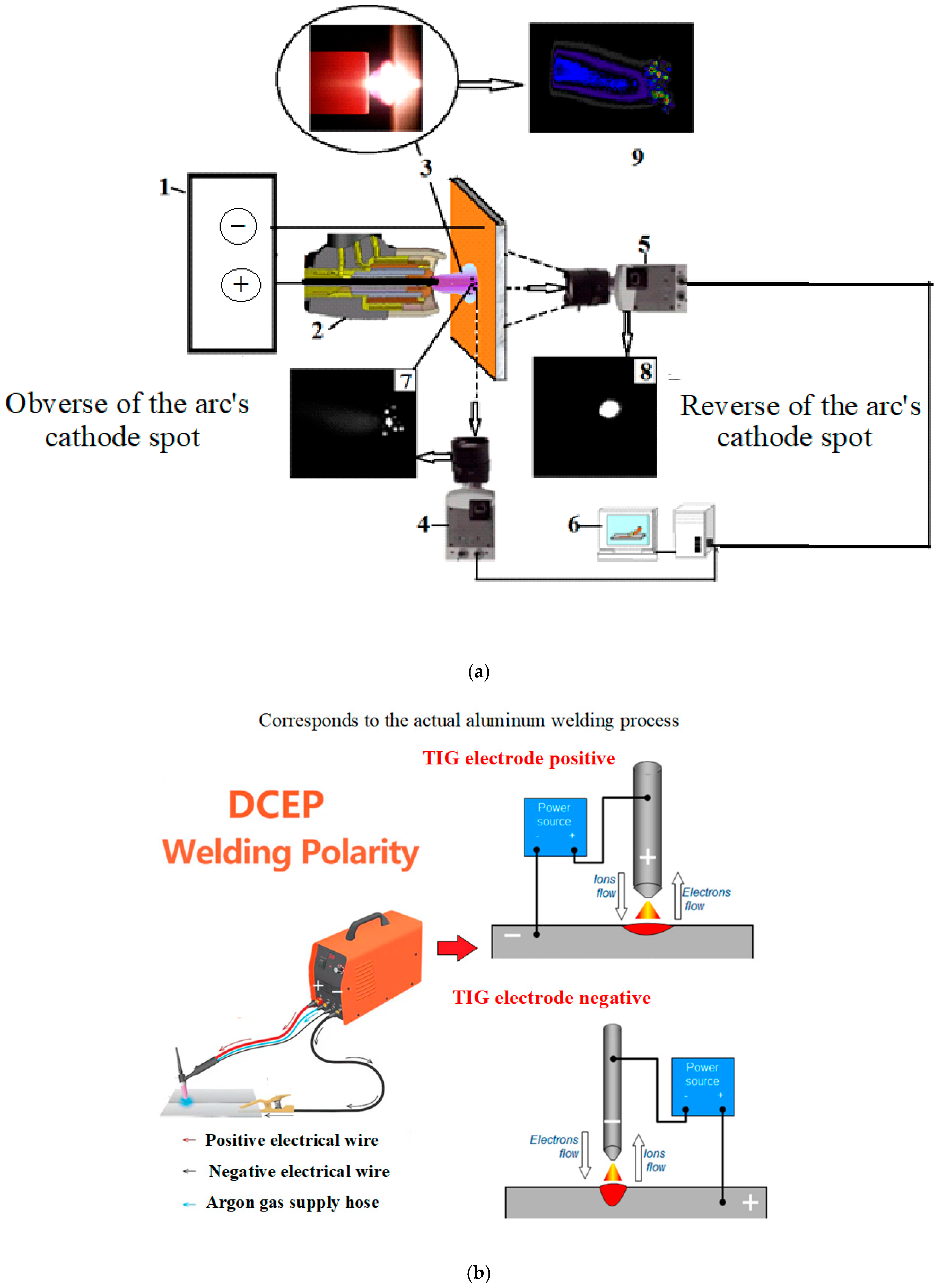
45]. The basic experimental setup is shown in
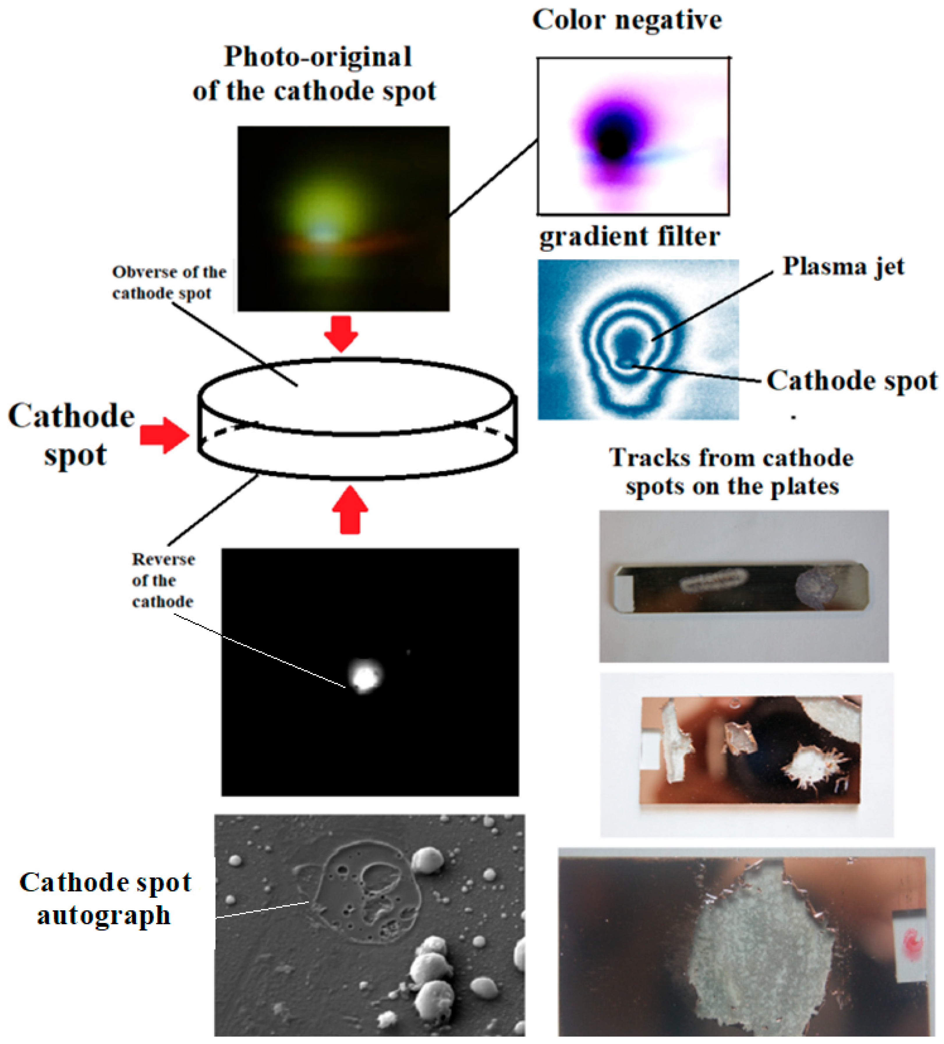
Figure 1, where the arrangement of two high-speed cameras is presented, allowing simultaneous recording of the front (obverse) and reverse sides of the cathode spot.
In the studies, samples with film cathodes were prepared by thermal evaporation in vacuum [
45] by depositing thin (10–350 nm) layers of copper, Al.Ti and other materials (silver) (
Table 1) onto soda–lime glass substrates measuring 25 × 60 mm and 2 mm thick, using the universal vacuum system VUP-5M. The deposition of the films was carried out at a residual gas pressure of P = 1 × 10
−8 Pa and a substrate temperature of T = 70 °C. All substrates underwent double preliminary cleaning: first, chemical etching in a chromic mixture solution (Na
2Cr
2O
7—100 g, H
2SO
4—50 g, distilled water—up to 1 L), followed by plasma-chemical cleaning using the Nano Clean “Model 1070” system (NanoClean, Budapest, Hungary). The thickness of the deposited films (
Table 1) was determined using microscopic and gravimetric methods [
36]. For the study of aluminum films, ready-made samples based on aluminum mirrors were used.
For the investigations, a direct-current welding arc of reverse polarity was used, with a current in the range of 2–160 A, burning vertically between a tungsten non-consumable electrode (diameter 2.4 mm) and the film cathode in an argon shielding gas environment. The arc burned in a stationary mode. The total arc burning time was 0.03–1 s.
A standard industrial welding power source with an open-circuit voltage of 60 V and a maximum current of 250 A was used as the arc power supply. To initiate the welding arc, a high-voltage spark discharge was employed, which is part of the standard equipment set for welding. At the location of the film, after the high-voltage pulse, the spark transformed into an arc [
52].
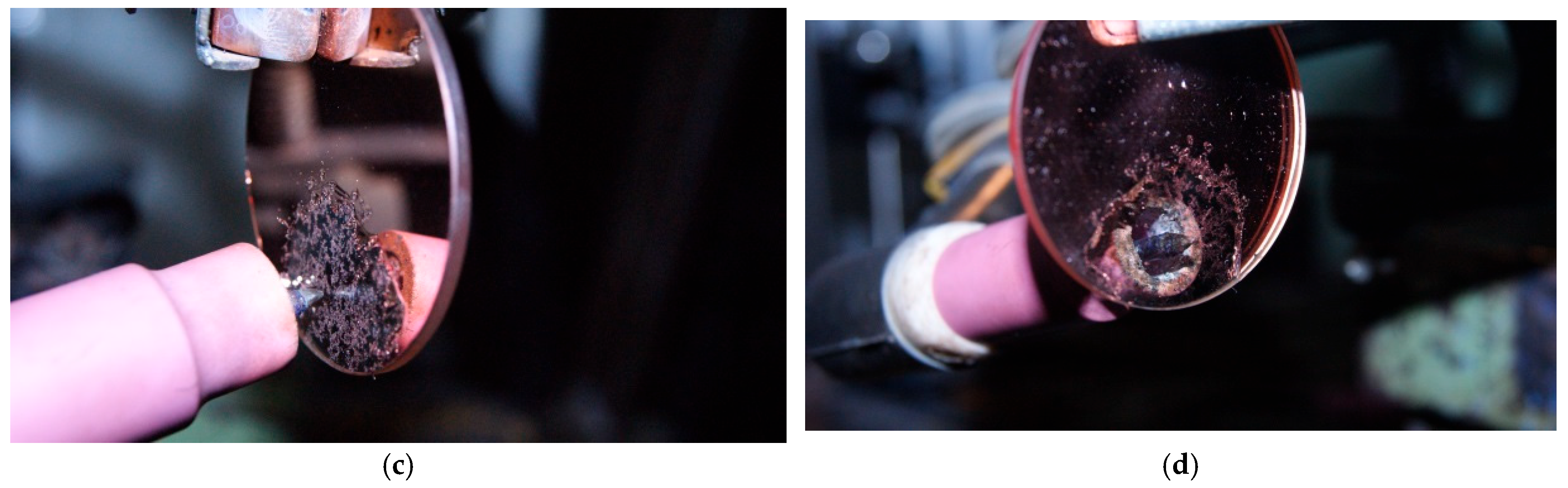
The cathode spot began to move chaotically across the surface, removing the metal film along its path and leaving behind distinct through-tracks (
Figure 2). The cathode spot has a front side with the cathode jet and a reverse side.
From
Figure 2 it is clearly seen that during the burning of the welding arc, the coating evaporates in the process of cathode spot formation, and traces of the cathode spot remain on the glass. The deposited coating serves as a protective screen, shielding the object of recording from the intense radiation of the arc column. It is evident that when recording the reverse side of the cathode spot, the high-speed camera will register only the radiation coming directly from the cathode spot after it has evaporated the film beneath itself, and this radiation can be decomposed frame by frame to allow accurate interpretation of the spatial dimensions of the cathode spot.
The arc length was varied from 0.5 to 5 mm. Time marks in the form of thickenings or stars [
12,
44,
45] were generated by superimposing periodic current pulses onto the direct current. Such marks made it possible to accurately identify the position of the spot in time and to calculate its movement velocity. An external magnetic field was not used to move the cathode spots, since according to [
12] it suppresses the cell-division process of the spot.
For recording the first series of experiments—sequential images during the act of arc burning—high-speed cameras were used: PCO.1200 hs and PCO.120 c, with a NIKON AF-S DX Zoom-Nikkor ED lens (NIKON, Tokyo, Japan), CMOS matrix (NIKON, Tokyo, Japan), pixel size 12 μm × 12 μm, resolution 1280 × 1024 pixels, exposure time range 1 ns–5 s, interframe time 75 ns, dynamic range 59.6 dB, and spectral sensitivity 290–1100 nm. The maximum recording speed at full resolution 1280 × 1024 was 501 frames/s. The maximum recording speed at minimum resolution was 32,000 frames/s at 128 × 16 pixels.
The PCO.1200 hs camera allows recording both in black-and-white mode and in color (by decomposing the optical image into brightness isolines). For recording the second series of experiments, the high-speed Phantom v711 camera was used, with a CMOS sensor resolution of 1280 × 800 pixels and a recording speed of 7530 frames/s. The throughput is 7 G pixels/s at a resolution of 1 megapixel, with a pixel size of 20 microns. The maximum recording speed is 1,400,000 frames/s. The minimum exposure time is 300 ns.
Before beginning the experiments, the cameras were synchronized with a central clock. This is achieved using the NTP protocol. All clocks on the devices display the same time, accurate to the millisecond. This process must be repeated periodically, as the devices’ internal clocks eventually begin to drift apart. After the clocks are “aligned,” the video cameras can embed time information (timecode) during signal transmission. We solved this problem using the SRT protocol and implemented the described methods in our SRTMiniServer version 2.6.2 (build 226) software decoder. When choosing a high-speed video recording system, one of the most important decisions is determining the required frame rate (FPS). For high-quality analysis, at least 10–20 frames must be captured during the object’s movement over a distance equal to its size. The formula is: FPS = (object speed)/(object size) × 10.
To calculate the FPS, we used known cathode spot parameters summarized in [
12,
13,
14,
15,
16]. The cathode spot speed is 10–100 m/s, and the cathode spot diameter is from 10 to 10 μm. Then, the calculation based on the formula shows that for a minimum cathode spot size of 10 μm and a minimum movement speed of 10 m/s, a camera with a frame rate of 100,000 fps is required. For a maximum spot speed of 100 m/s and a maximum cathode spot diameter of 100 μm, a camera with a frame rate of 50,000 fps is sufficient. The cameras presented above, used in our experiments, allow shooting at a frame rate of up to 150,000 fps. The cameras we used have a region of interest (ROI) function, which allows us to increase fps by reducing the active area of the matrix. This is especially useful when you need to focus on a specific area without losing speed. For example, using an ROI of 50% in width and height, the frame rate can increase by 4 times.
The object was photographed with file recording in an uncompressed format (raw format), which was transferred to a computer, and the file was converted into TIFF format (R, G, B). Each channel of this file was then saved as a separate TIFF file in 8-bit grayscale, with the output signal in the range of 0–255 pixels for each channel. Standard software packages Adobe Photoshop C3 CC 2018 (version 19) and Lightroom Classic were used for computer processing.
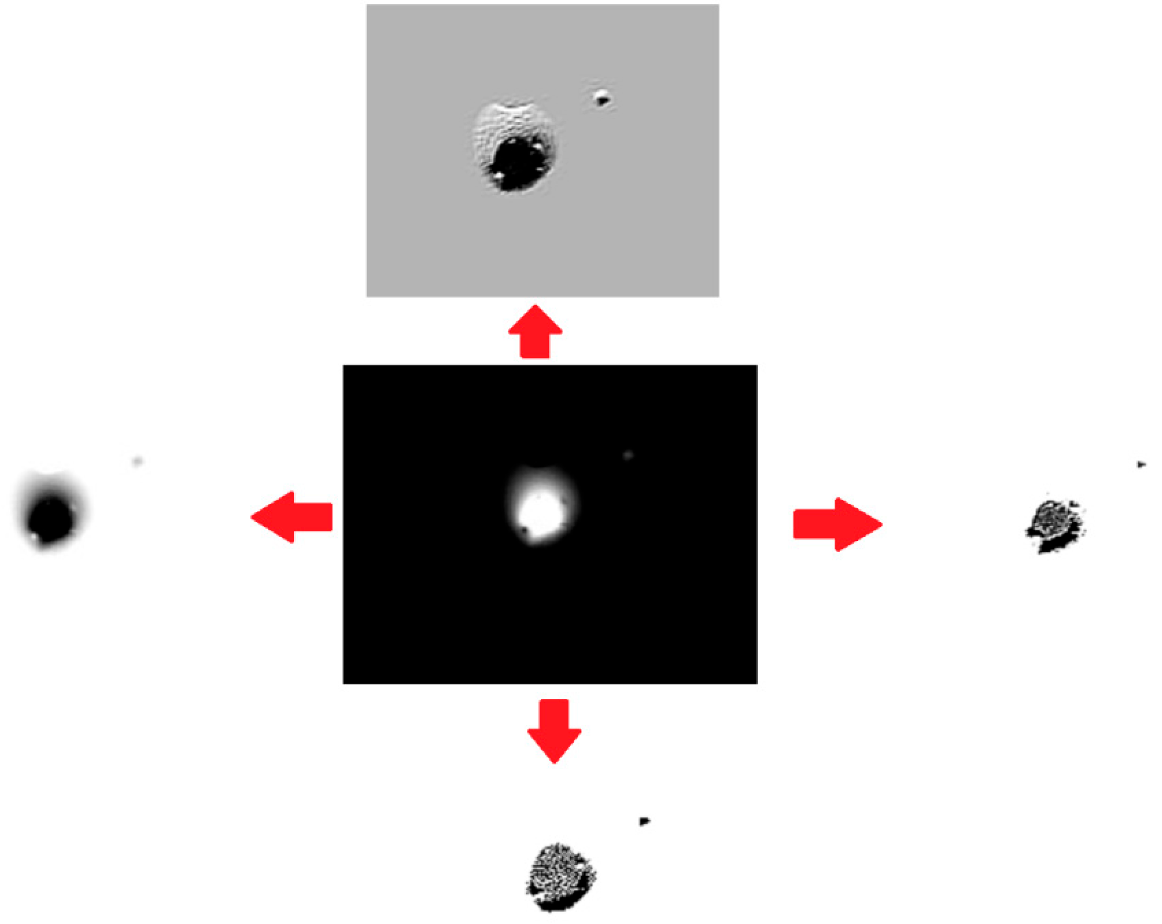
The input image is assumed to be matrix A, whose elements are the pixel brightness values, with dimensions MxN. An 8-bit Grayscale format is assumed. In the case of a 24- or 32-bit image, the color background responsible for its position in the spectrum is removed for conversion to grayscale format. Adobe Photoshop C3 has built-in software mathematical modules. Let z = f (x, y) be the discrete brightness distribution function of image A. Here, X represents the columns and Y the rows in the image matrix. It is necessary to find the direction of greatest brightness increase and the magnitude of its change in this direction—in other words, to find out how “sharply” or how “smoothly” the brightness changes at each point, and therefore to determine whether the point is on the edge. Thus, below we will discuss the derivative of the brightness function f (x, y), which characterizes the rate of its change at each point. Analysis of gradient methods is based on image convolution, an approach based on convolution of the original image with a mask (operator) centered at a point with x and y coordinates. This process is repeated for each filter. Let us consider well-known operators that use masks to calculate the approximate value of the image brightness gradient at a specific point. The Roberts operator is a simple version of calculating a discrete gradient. Its construction exploits the fact that derivatives (differences) in any two mutually perpendicular directions can be used to calculate the gradient modulus. Other operators include the Pruitt operator, the Sobel operator, and the Scharr operator. Let us compare the processing of a simple image with blurred light (
Figure 3).
Based on the results, the following conclusions can be drawn:
- –
The gradient directions are close to those of the Pruitt and Sobel operators.
- –
The Roberts operator better identifies edges than finite difference methods. However, it is less effective at determining gradient directions.
- –
The Scharr operator excessively identifies edges. The gradient value is overestimated compared to the operators discussed above. The direction angle is close to that of the Pruitt and Sobel operators. Therefore, we use only two filters with caution: brightness, contour, and inversion (negative).
Please note that our article is not about Adobe Photoshop C3 software.
The image quality (objective shooting characteristics) was evaluated using the results of photographing a Kodak Q13 (Rochester, NY, USA) test target and a test chart (65 × 45 cm, full-frame imaging) to verify resolution, distortion, and chromatic aberrations. The methodology for calibrating brightness and color pyrometric systems based on CCD matrices is currently well developed [
41,
42,
43,
44,
45]. Temperature calibration of digital cameras was carried out using a CI-8 lamp by varying the lamp filament current and recording the temperature. The temperature resolution under this calibration is 1.2–1.8 K.
In conducting the experiments, it was assumed that measurement errors can be divided into three parts: systematic errors of the brightness pyrometry method; errors related to camera calibration; and direct measurement errors. For this reason, an assessment of measurement error was performed following the methodology of works [
35,
36,
37]. The estimated measurement error associated with inaccurate camera positioning, noise from the object, and CCD matrix noise amounted to 4–6 K. The measurement error of brightness temperature in our experiments was 15–30 K.
The standard software packages Adobe Photoshop C3 and Lightroom were used for computer processing. The visualization methodology and image processing procedures are described in detail in [
43,
44,
45]. In addition, methodological recommendations for image evaluation presented in works by other authors were taken into account [
13,
14,
16,
19,
20,
21,
22,
23,
24,
25,
26,
27,
28,
29,
30,
31].
For current and voltage measurements, a Tektronix TDC-1012 digital oscilloscope (Beaverton, OR, USA) was used. The surface of the film cathode after exposure to the welding arc was examined using an Altami MET 1T metallographic optical microscope (Tokyo, Japan) and a JEOL JIB-Z4500 scanning electron microscope (Tokyo, Japan).
3. Results
In
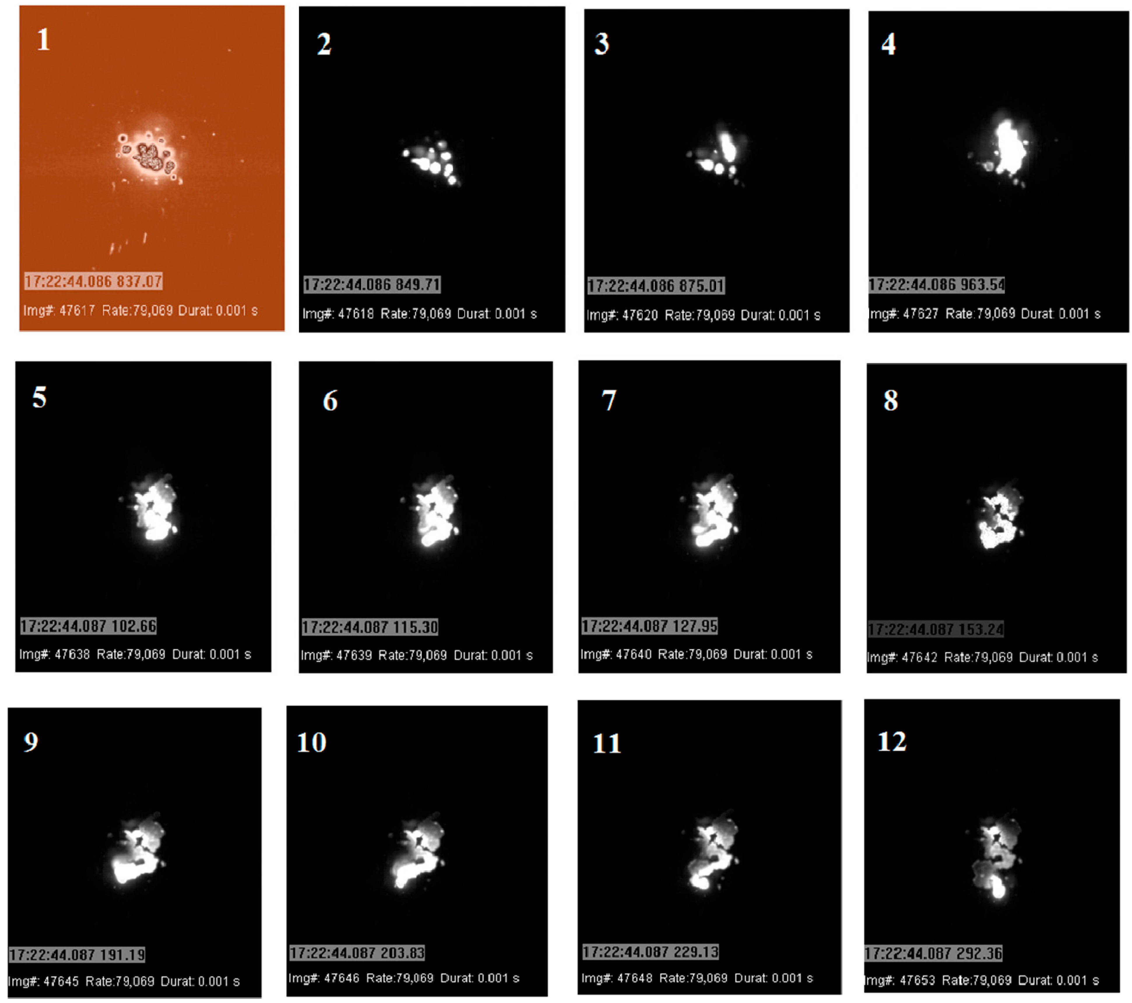
Figure 4, a frame-by-frame decomposition (time between frames 0.0025 s) of the formation of a cathode spot on the surface of a silver film with a thickness of 100 nm is presented. The arc burned in a stationary mode. The welding current was 30 A. It can be seen that at the initial moment of image registration from the reverse side, several cathode spots were recorded directly in the center of the frame (
Figure 4, positions 1 and 2). Within the circular area, seven bright point-like objects and two dimmer objects—presumably also point-like—are observed.
Further, in
Figure 4, positions 3 and 4, the pattern changes, as the cathode spot begins to move upward and merges into a single group spot. At the same time, the contour area of the overall heated region is preserved, and point-like objects of lower brightness become visible, which in the previous frames (
Figure 4, positions 1, 2, 3) were brightly illuminated.
With increasing arc burning time, in
Figure 4, position 5, the cathode spot sharply changes direction and begins to move in the opposite direction. The contours of the track of cathode spot motion clearly appear within the movement area.
In
Figure 4, positions 5, 6, 7, 8, 9, 10, and 11, it is seen that the area of the heated spot remains almost the same throughout the entire path of motion, and as the film evaporates under the cathode spots, fragments of the film that did not fall within the active spot zone become visible. Around the brightly glowing regions of the meandering motion track, dark contours of the silver film are clearly seen.
In
Figure 4, position 12, it is clearly visible that the diameter of the glowing spot has stabilized, and apparently it has already become a single cathode spot. We see that during the motion of the spot, a large portion of the film within the contour of the heated spot has evaporated, leaving a distinct track of motion.
The photographs in
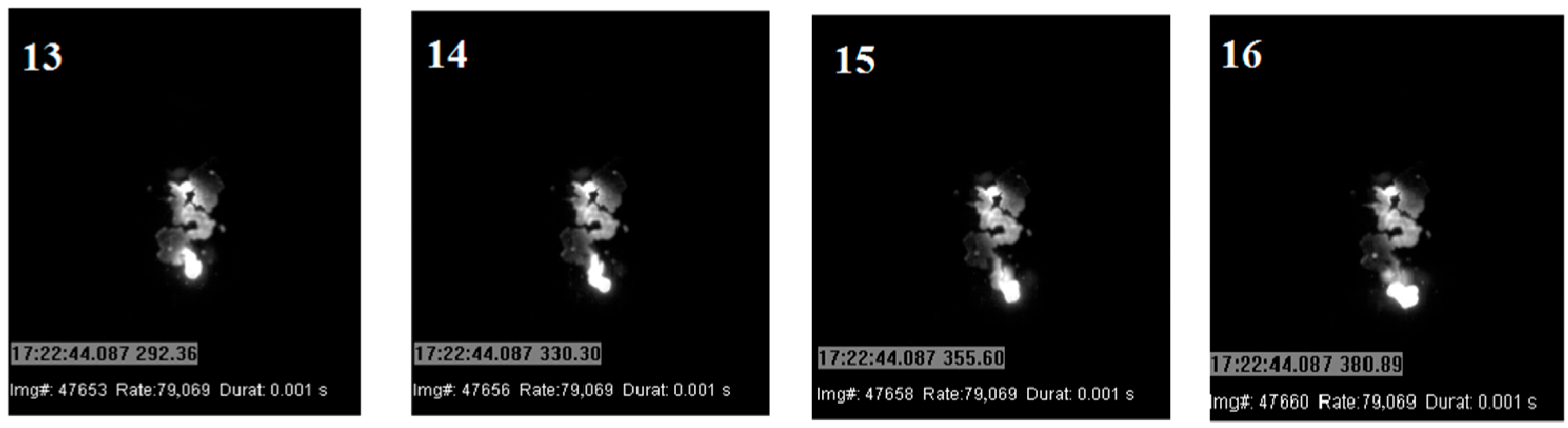
Figure 4, positions 13, 14, 15, and 16 show the motion of a single spot. As noted in [
4,
36,
37], with increasing film thickness, the spot track becomes extremely non-uniform in width, and isolated inclusions of unmolten metal remain on the exposed glass areas in the form of islands, indicating the presence of several cells within the spot.
Such behavior of the cathode spot indicates that the power delivered to the cathode undergoes temporal variations due to changes in the operating mode of the cells. It is possible, according to [
4,
36,
37], that the un-melted regions of the film correspond either to the moment of cell division or to a deceleration of their motion. This can be seen in more detail in the
Supplementary Materials (Video S1 and S2).
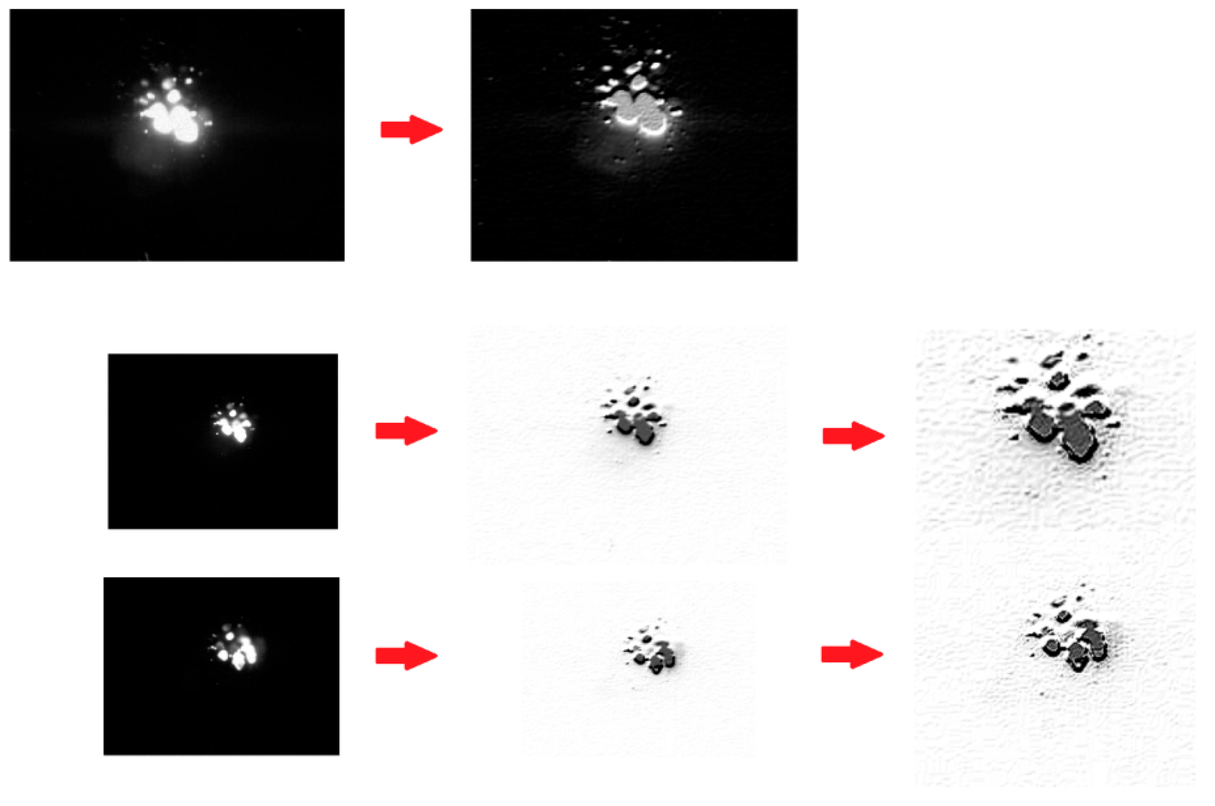
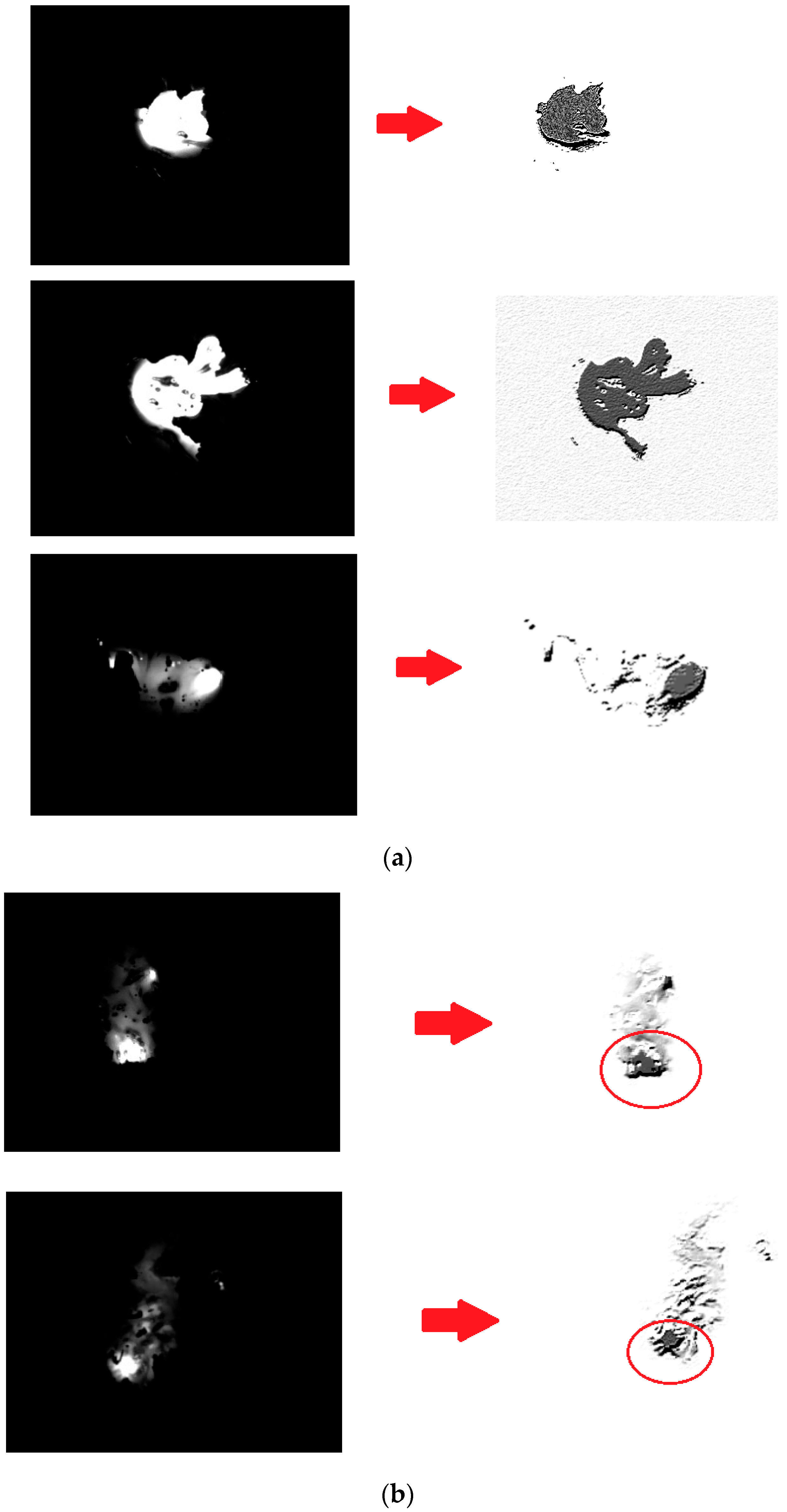
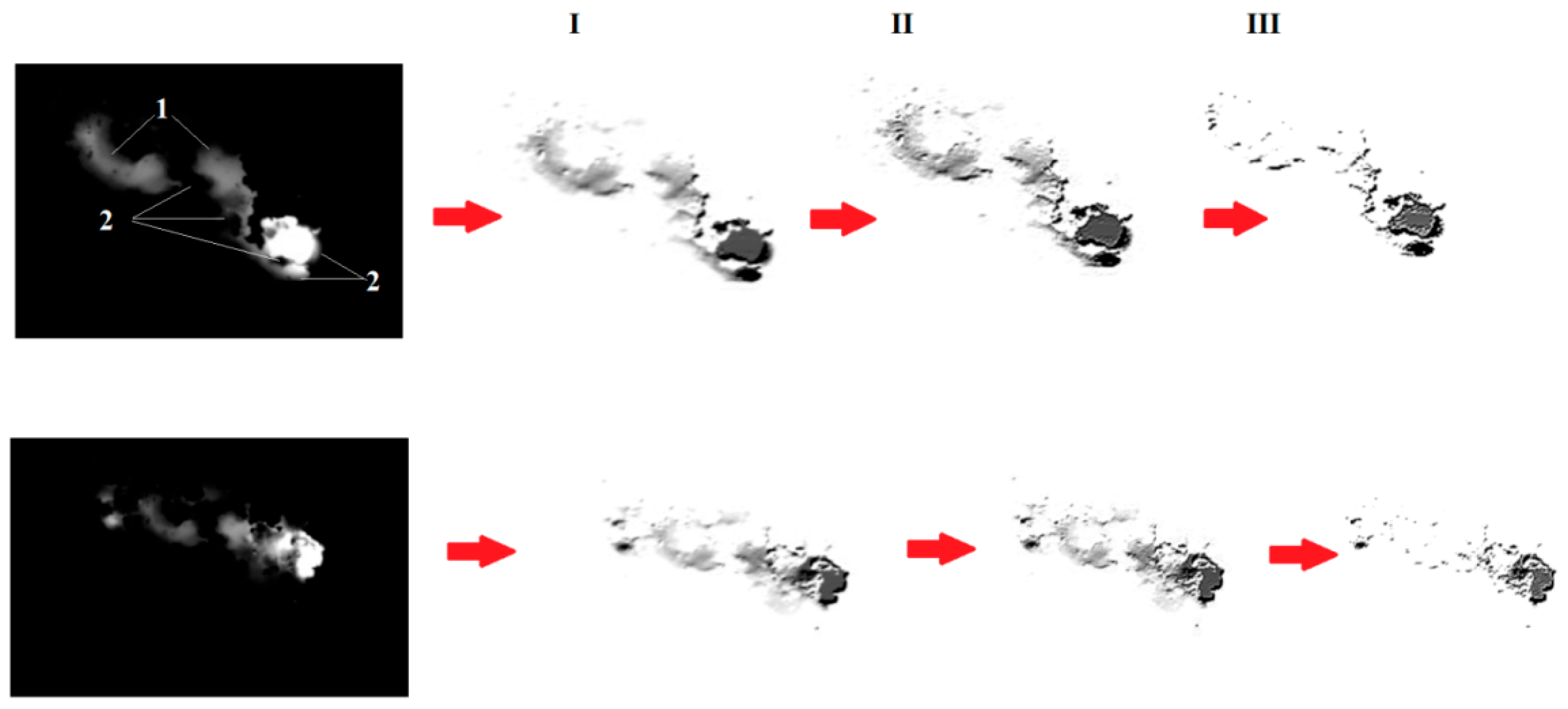
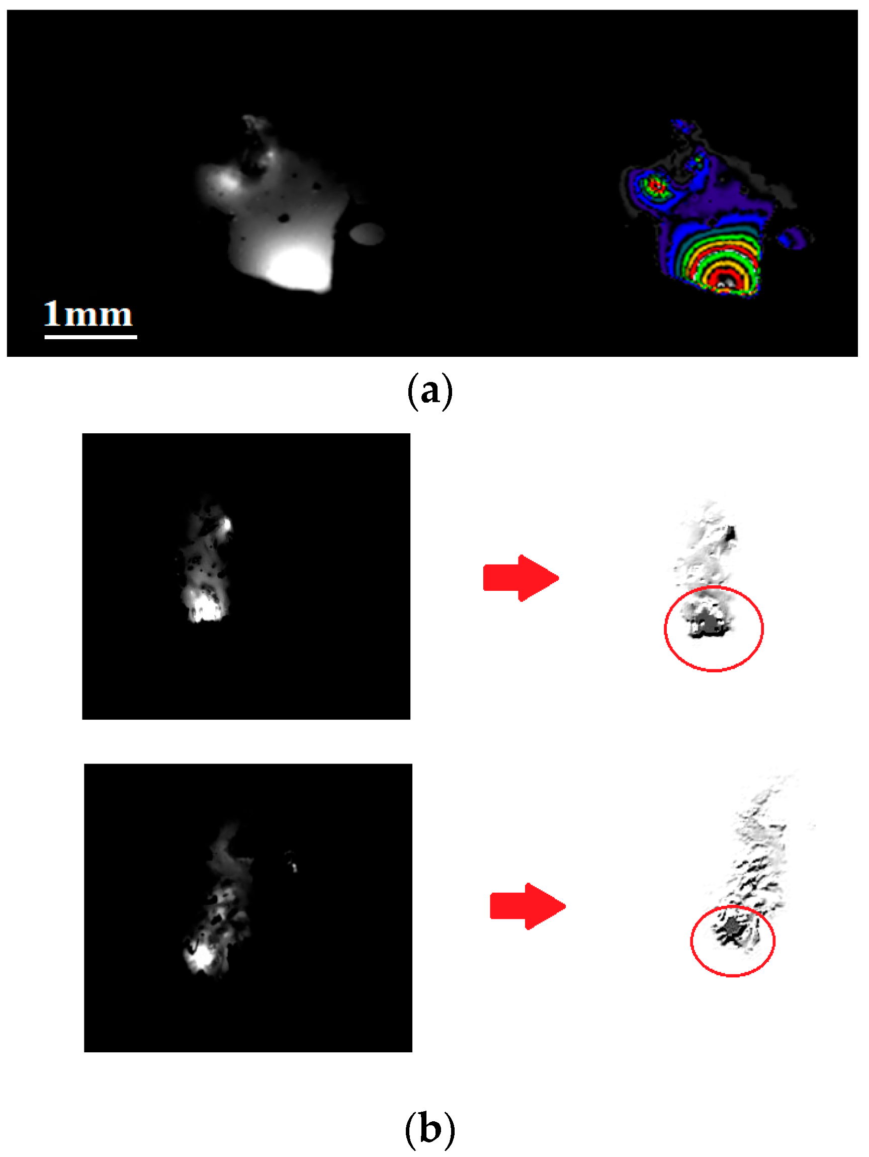
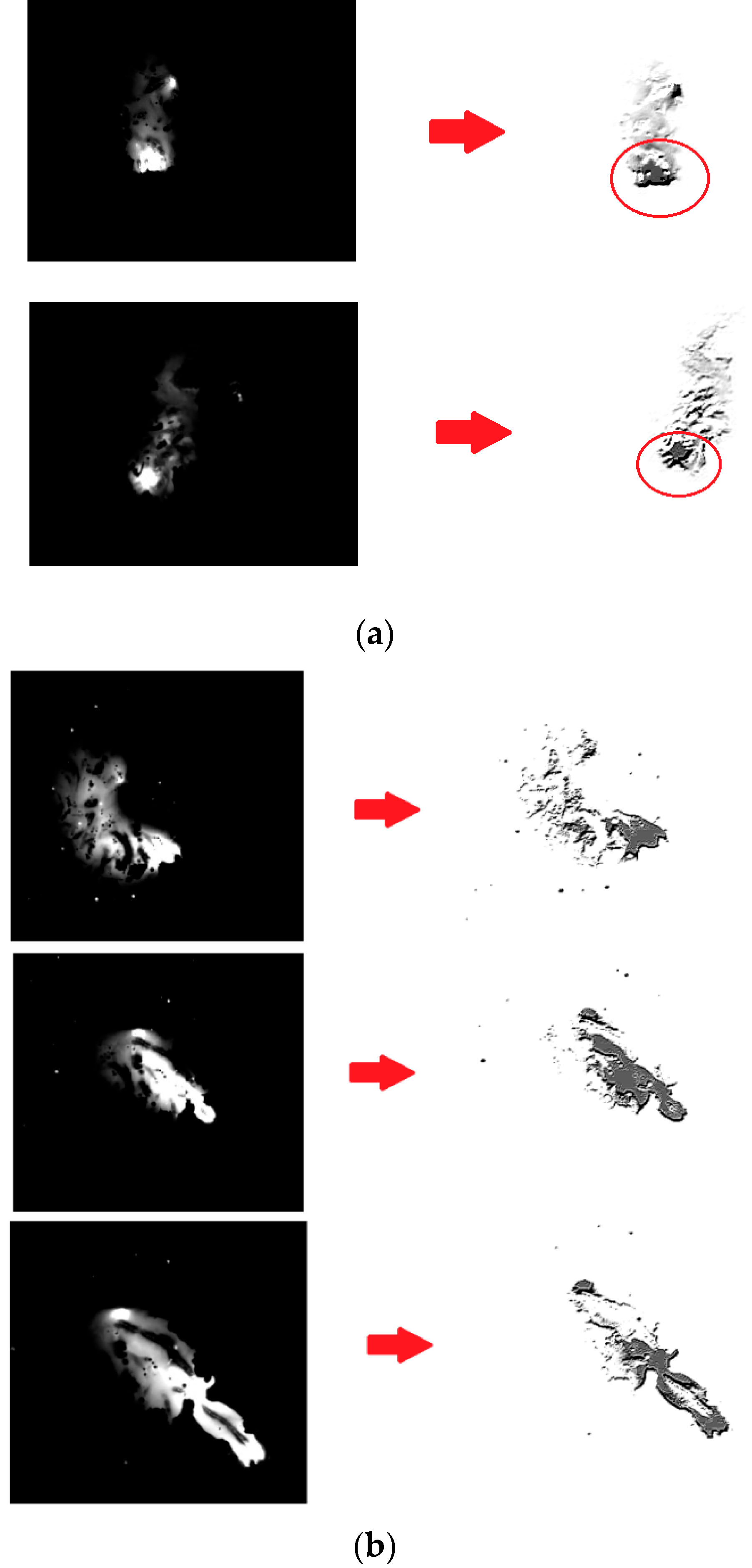
Thus, we can interpret the bright, glowing, moving point-like objects not only as cathode spots, but also as an experimental confirmation of the visualization of the reverse side of cathode spots. During the processing of optical images of the reverse side of the cathode spot, the following image-processing algorithm was applied using Adobe Photoshop C3 (
Figure 5). In the original image (
Figure 5), the analysis regions are identified: region No. 1 corresponds to the cathode spot track, and region No. 2 corresponds to the film edges and the non-evaporated portion of the film. The main object—the cathode spot, the bright area in the original image—is processed in three stages.
At the first stage, the image is converted to a negative, where the cathode spot becomes clearly visible. At the second stage, a sharpening filter is applied, which immediately delineates the boundaries of the optical region of the cathode spot. At the third stage, a texture filter is applied, producing the processed image of the cathode spot.
The lower image in
Figure 4 shows the processing algorithm for a group cathode spot.
In
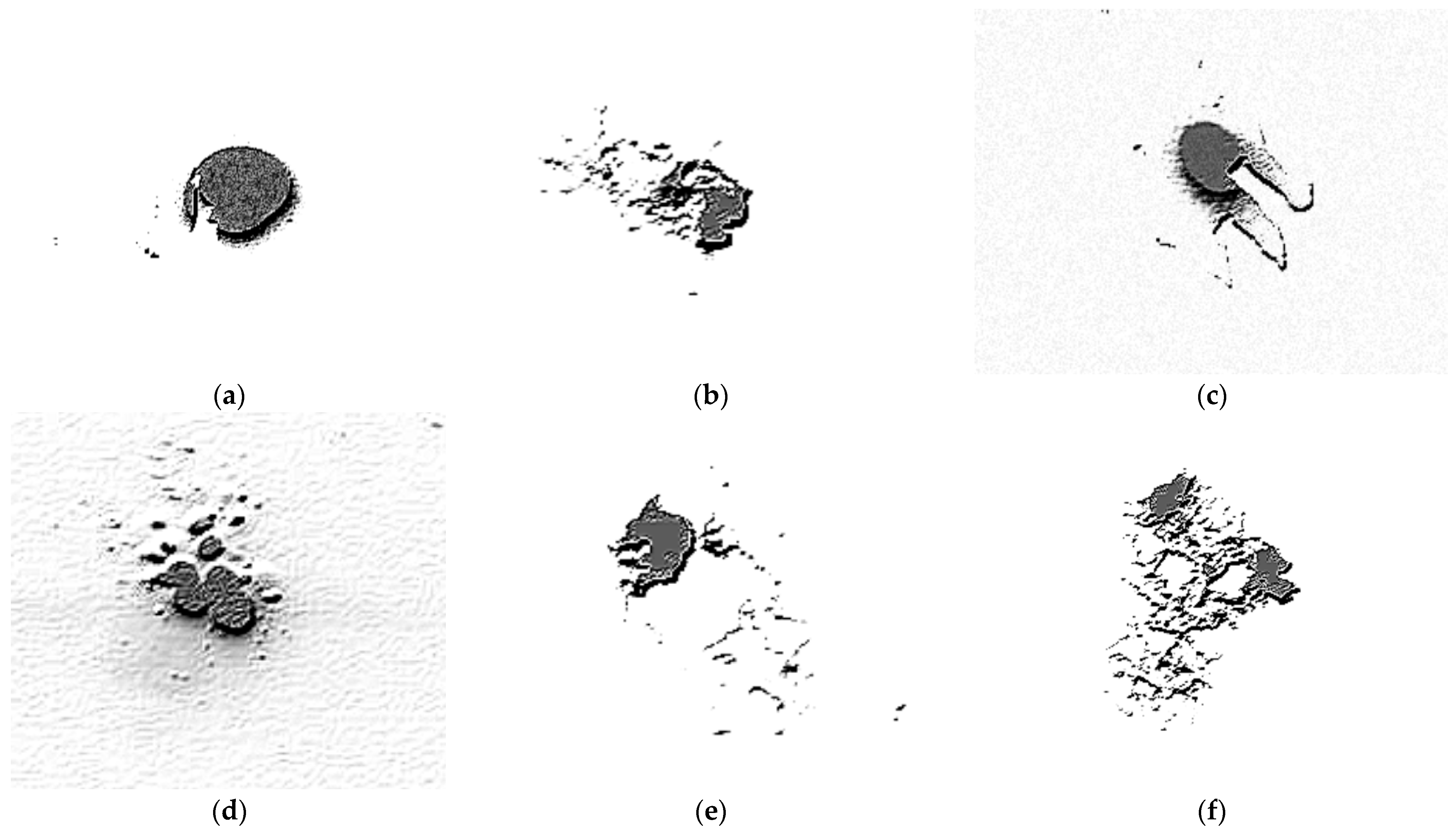
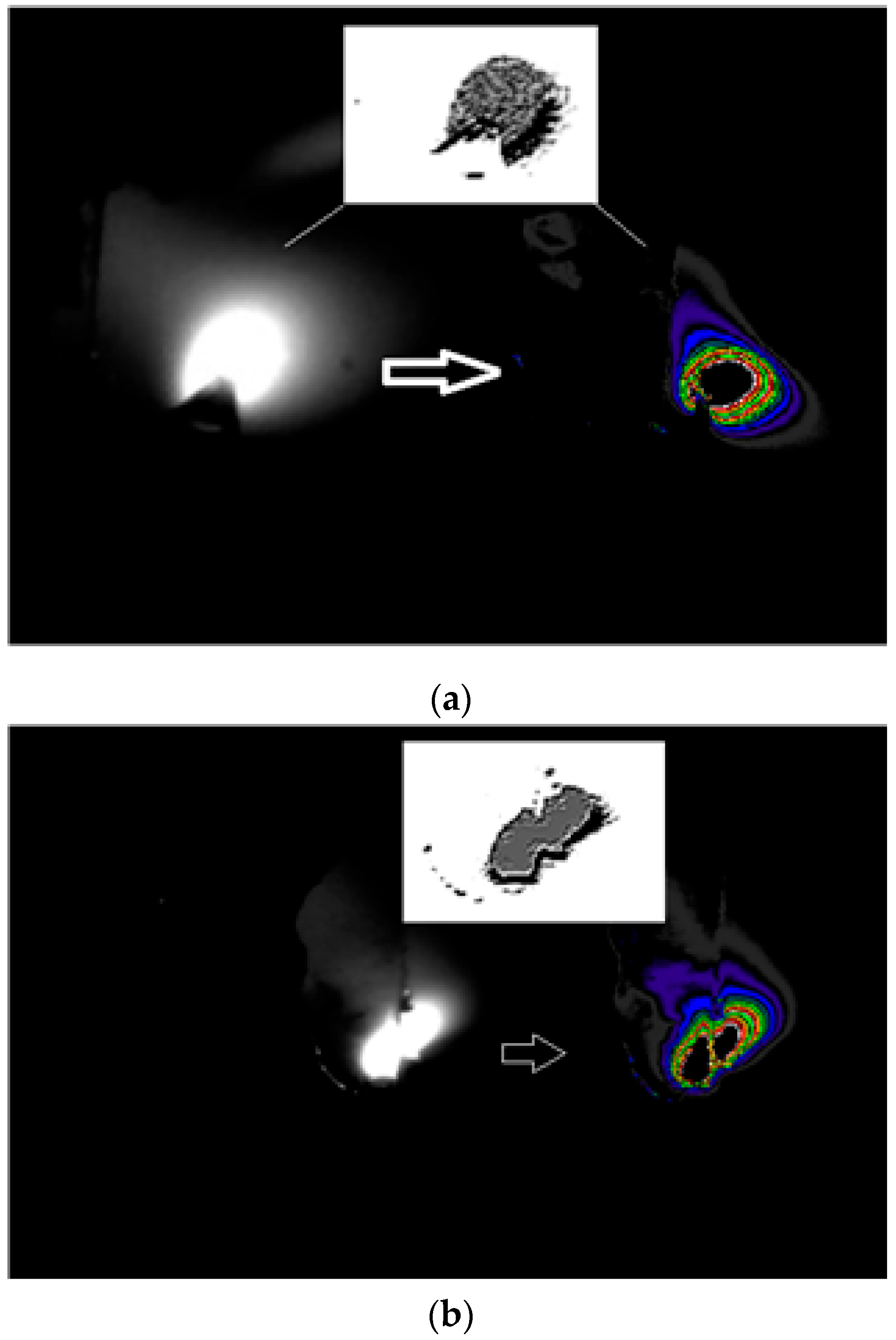
Figure 6, comparisons of the results of processing the optical image using different filters are shown. The optical image of the reverse side of the cathode spot is placed in the center. By applying various specialized processing filters, we can obtain an idea of the internal structure of the cathode spot. In
Figure 7, the results of the formation of a cathode spot on the surface of a copper film with a thickness of 30 nm are presented. The arc burned in a stationary mode. The welding current was 10 A. The photograph (
Figure 7) shows that the required number of cells is not created immediately, but through several cycles of division. The division process is preceded by an increase in the transverse size of the track during spot motion.
Attention is drawn to the fact of localized film evaporation at the locations of cell movement within the cathode spot. In the color image at the bottom, the dark regions (fragments of the film) are clearly visible.
During the experiments it was established that, with increasing film thickness, the spot track becomes extremely non-uniform in width, and isolated inclusions of unmolten metal remain on the exposed areas of the glass in the form of islands, indicating the presence of several cells within the spot. Such behavior of the cathode spot indicates that the power delivered to the cathode undergoes temporal variations due to changes in the operating mode of the cells. It is possible, according to [
35,
36,
37], that the un-melted regions of the film correspond either to the moment of cell division or to a deceleration of their motion.
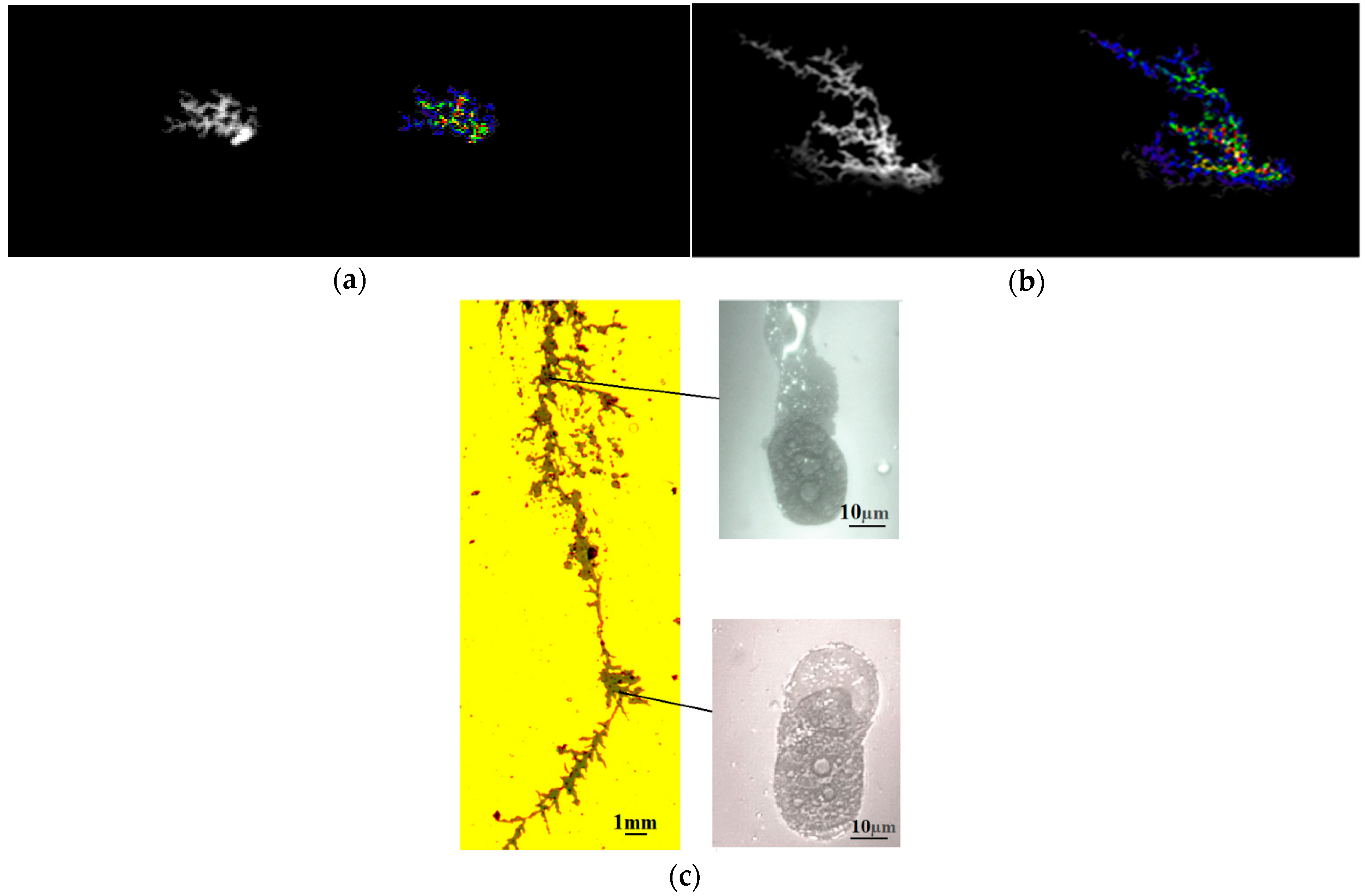
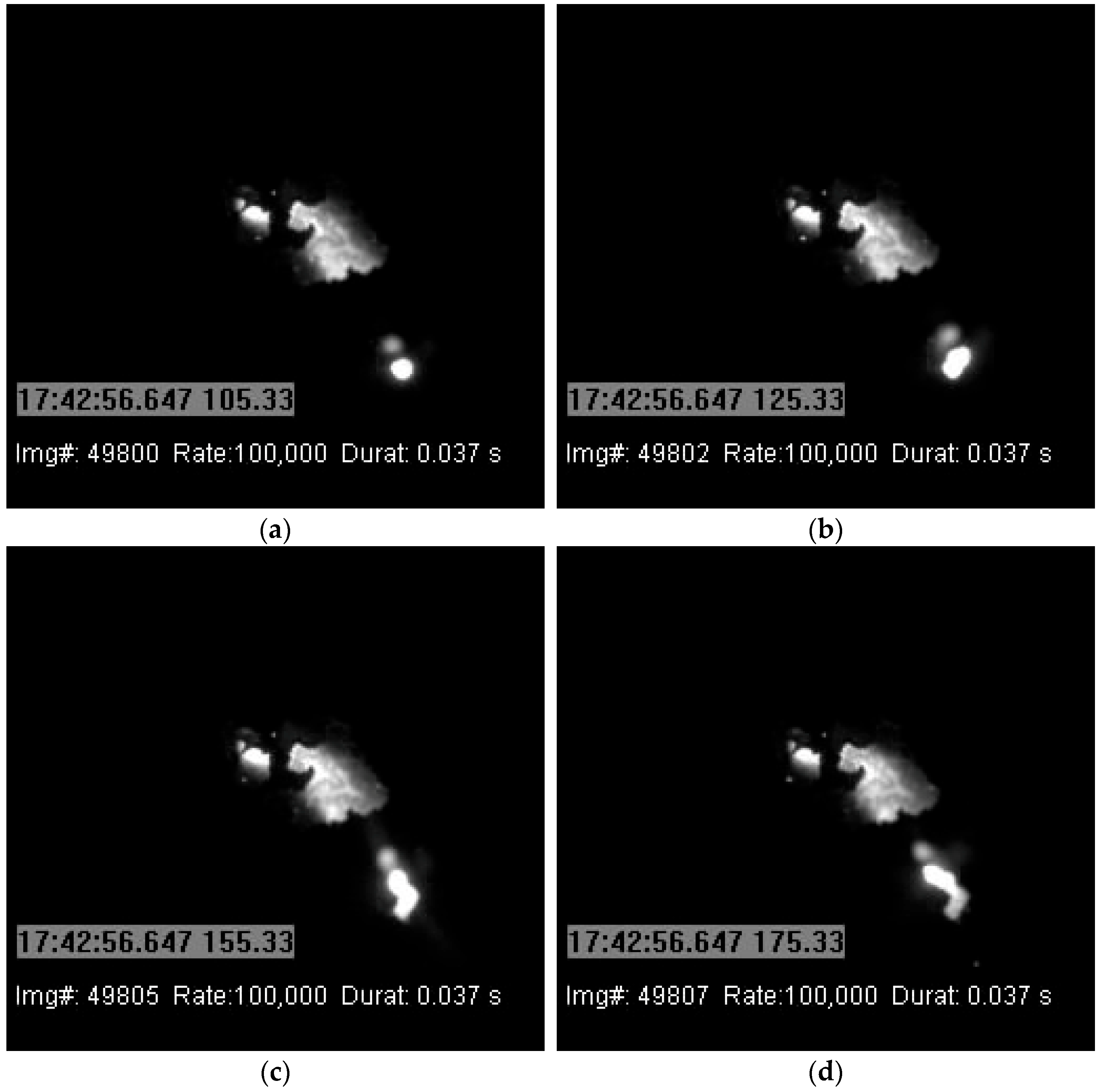
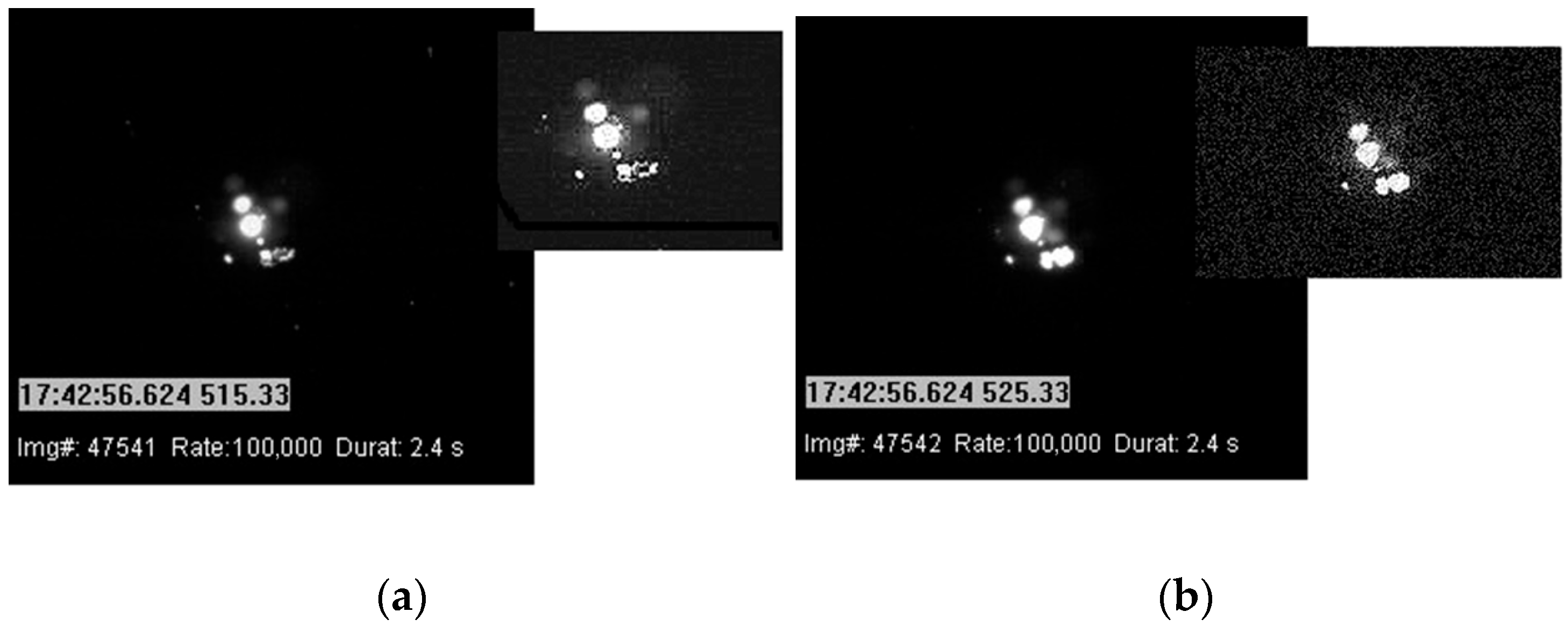
On samples with a copper film thickness of 140 nm, using a recording rate of 100,000 frames/s, we observe the formation of a single cathode spot on the surface of the copper film (
Figure 8).
In
Figure 8a, the formation (anchoring) of the initial cathode spot is clearly recorded in the lower corner, after which it moves, removing the film beneath it (
Figure 8b–d). A sharp change in the direction of motion (almost by 90 degrees) is observed in
Figure 8b,c. The velocity of the cathode spot motion was 150 m/s.
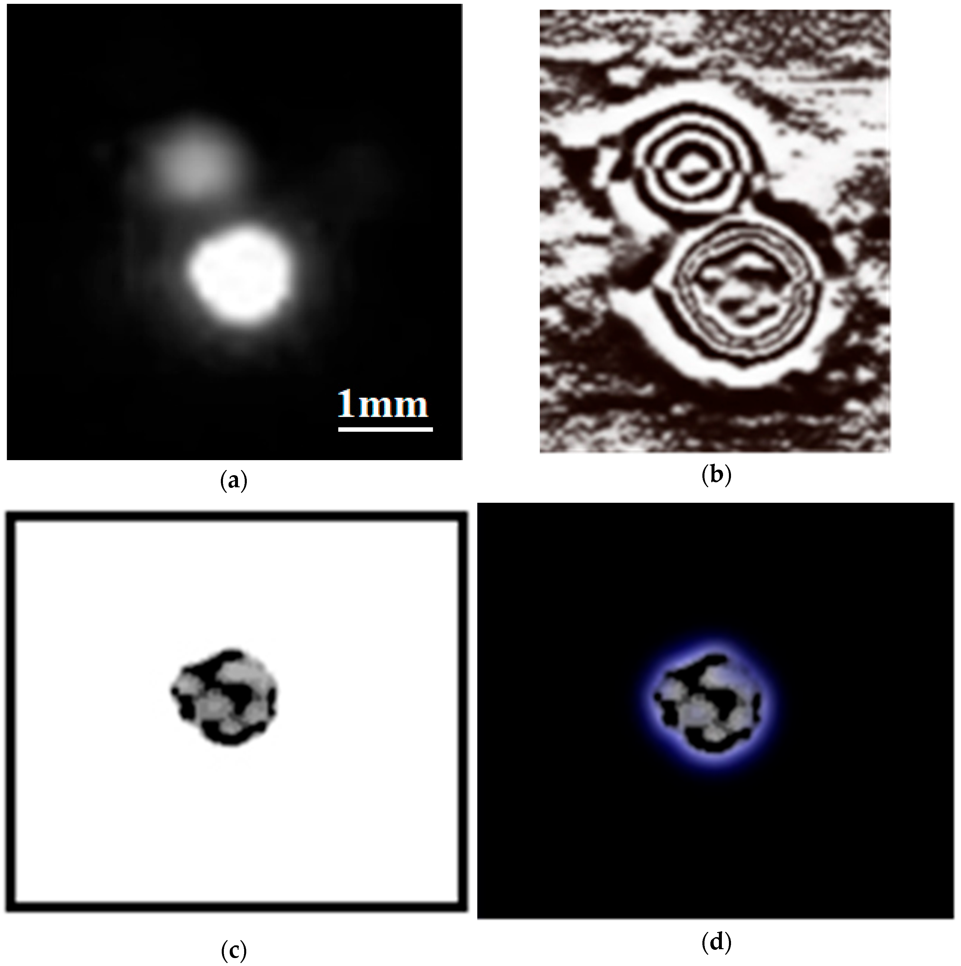
The optical images of the reverse side of the cathode spot obtained by us in the course of the experiments (
Figure 9) were processed using well-known image-processing software. Relief filters were applied (
Figure 9b), as well as the negative-of-negative filter (
Figure 9c) and the brightness-density gradient filter. This made it possible to obtain new qualitative information about the internal structure of the reverse side of the cathode spot.
In
Figure 9a, the internal structure of the reverse side of the primary cathode spot from the frame in
Figure 8a is shown. In
Figure 9a, from the luminous spot, it can be seen that at the formation stage the cathode spot has a circular shape, inside which additional formations are observed. Converting the image using the relief filter immediately provided a qualitative representation of the cathode spot structure (
Figure 9b) in the form of a circular spot containing internal segments.
When processing the image in
Figure 9a with the negative filter, the black-and-white image in
Figure 8c was obtained, showing the internal structure of the cathode spot. Then, using the brightness-gradient filter, the image in
Figure 9d was obtained.
Overall, the reverse side of the cathode spot (based on the color distribution of brightness-density regions within the spot area) has a granular structure. The area of the internal-structure regions of the reverse side of the cathode spot is significantly smaller than the luminous area in the unprocessed image. It may be assumed that these internal structural segments of the spot are the ones producing the intense radiation.
The image of the reverse side of the cathode spot turned out to be so successful that there was practically no need to analyze it using Adobe Photoshop C3. It was sufficient to apply a texture filter for the structure of the cathode spot to appear. Subsequently, we performed processing according to the algorithm described above, and it can be seen that this is a group of cathode spots.
In
Figure 11 and
Figure 12, the results of image processing are presented, showing the formation of the cathode spot in time (
Figure 11) and the shape and internal structure of the cathode spot from the reverse side, both in the stationary state and in dynamics. It is evident that when the cathode spot is stationary, its shape is closer to circular; as soon as the spot begins to move, its shape changes and becomes fragmented (
Figure 12).
In the color image (
Figure 11), the discrete structure of the reverse side of the cathode spot is visible. It can also be seen that during the motion of the cathode spot, the width of the track is smaller than the diameter of the spot. Since the recording was carried out in the frontal plane, the frame with the heated spot (
Figure 11c) registers only a planar measurement and does not convey volumetric details. If one proceeds from the width of the track formed during spot motion, then the true diameter of the reverse side of the cathode spot is smaller than what is observed in the image. A well-known feature reported in many studies using the classical autograph method [
4,
35,
36]—the meandering, chaotic nature of the tracks left by the cathode-spot cells on the film surface—is also preserved in the visualization of the reverse side of the cathode spot. However, there exists a “conditional leader” among the cells, which determines the general direction of motion and groups their chaotic movement within a confined area.
If a circle is placed on the black-and-white image in
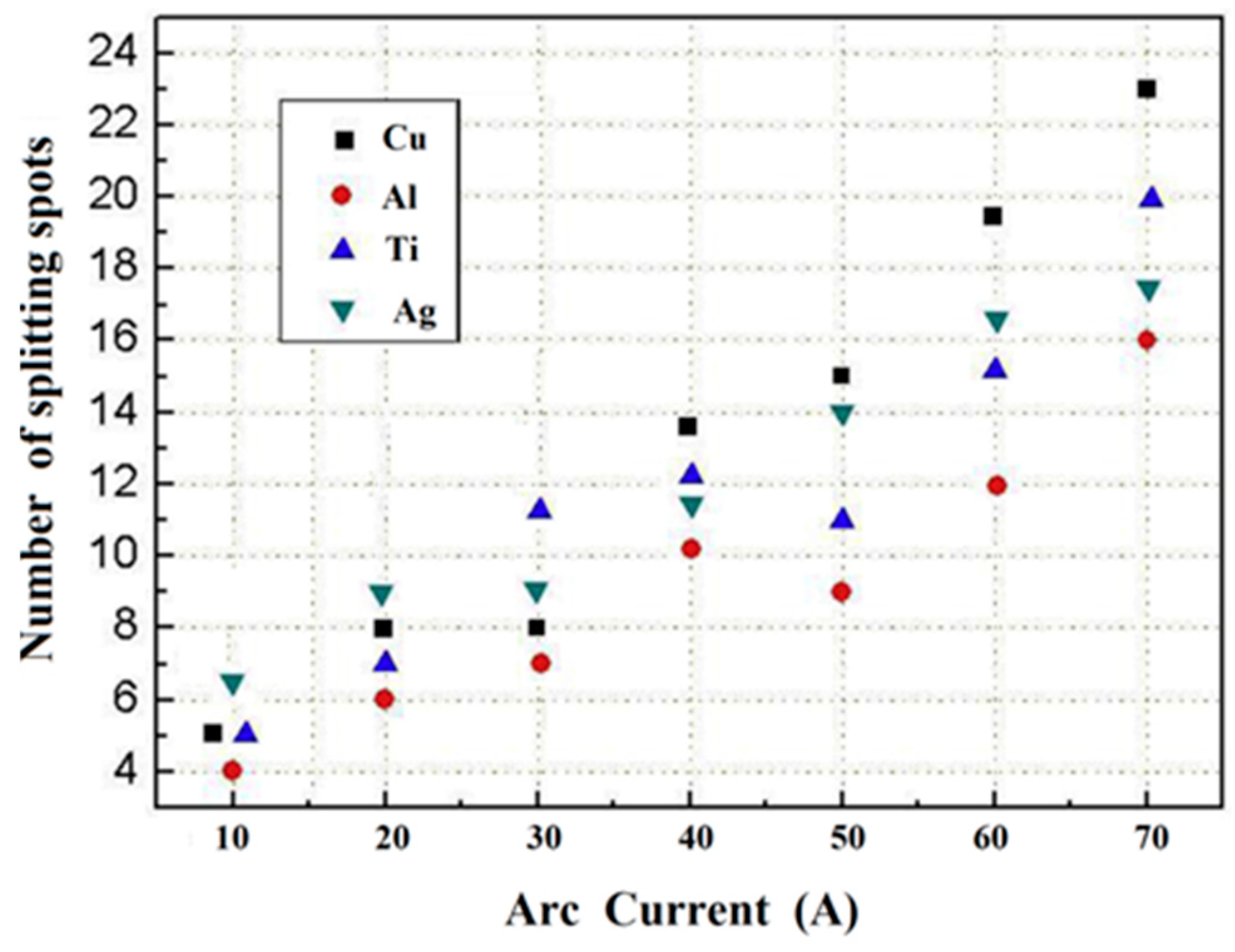
Figure 11c along the bright luminous zone corresponding to the motion of the spot, it becomes evident that a discrete internal structure appears within the spot area. In the color image, a point-like structure of light within the circular region is visible, indicating the existence of an internal discrete structure of the reverse side of the cathode spot. We view this statement with a certain degree of caution, as we will attempt to further refine our image processing method. In the course of the experiments, it was established that with increasing exposure time and current, the number of cathode spots increases (
Table 1,
Figure 13 and
Figure 14). The lifetime of the cathode spots is influenced by the film thickness. In all cases, for equal film thickness, current, and arc burning duration, the average lifetime of the cathode spots increases.
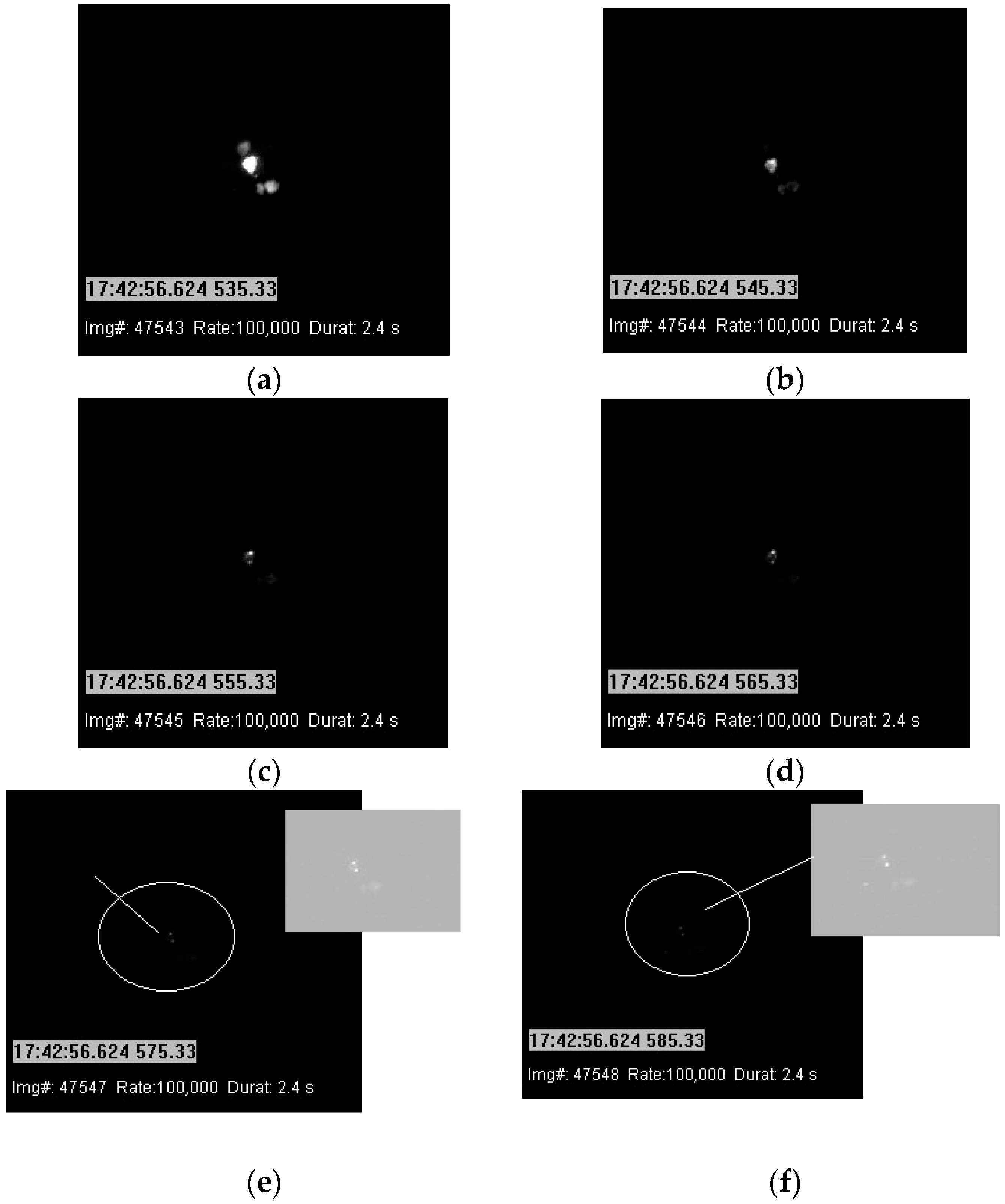
In the images obtained in our experiments, the back side of the cathode spot undergoes the same processes as when photographed from the front side, including the sequential ignition of a new spot and the extinction of an old one. To clearly determine these characteristics, it is necessary to use an appropriate exposure time. Theoretically, the exposure time for an image should be set as short as possible to prevent image blurring due to spot movement. We conducted an additional series of experiments with different exposure times and an appropriate interval for spot dynamics. Initially, an interval of 1 ms was set for spot images, extracted from the recorded video. The effects of longer intervals and longer exposure times were then also examined. After recording dynamic videos of cathode spot movement under various parameters, images from each video were extracted using post-processing software at an interval of 1 ms. To test the reproducibility of the results, three groups of images were randomly selected for each video and compared with each other under the same conditions. About 10,000 images without magnification were extracted from each video, after which the characteristics of the cathode spot backside were compared under different parameters. Using long exposures, groups of 400, 600, and 800 images (with corresponding intervals of 5 ms, 10 ms, and 20 ms) were also extracted from the same video, and these photographs were also compared with the cases with an interval of 1 ms. We compared a series of sequential images of the cathode spot backside at currents of 10 A, 30 A, 50 A, and for 30 ms at exposure times ranging from 0.01 ms to 0.25 ms. It was found that the cathode spot ignites and moves stably. At a minimum exposure time of 0.01 ms, it is difficult to distinguish a group of spots or fragmentation in the spot in the images, especially at an arc current of 10 A.
However, with an increase in the exposure time to 0.04 ms, the process of division into microspots is clearly visible in the images at all values of the arc current. With an increase in the exposure time to 0.08 ms, the results are almost the same. The effect of exposure time on the observation results is due to both the distance the cathode spot moves and the merging of microspots. It is important to understand that exposure time is a duration. The spot moves at a speed of 10–100 m/s during the arc process [
12,
13,
14,
19,
20,
21,
22,
23,
24,
25,
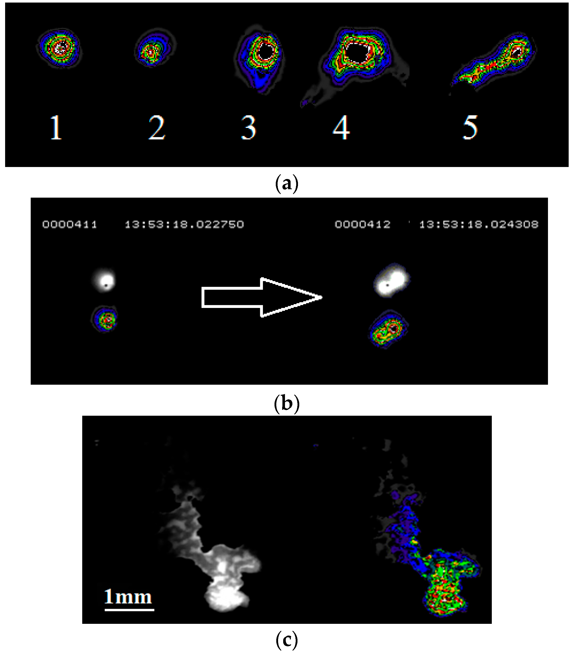
26]. And this will determine the frame rate and the movement of the spot in the focal area. It can be assumed that the longer the exposure time, the further the cathode spot moves. It is possible that the processes of division and merging occur not sequentially, but in parallel. Then the cathode spots cannot move in a stable direction, as a result of which either a larger bright spot appears in the image, as shown in
Figure 11a (No. 1,2,3,4), or a stretched one,
Figure 11a (No. 5). The number of cathode spots depends on the arc current (
Figure 12). As the current increases, between 4 and 22 can be detected, depending on the cathode material. Based on our statistical analysis of the images, shorter exposure times are desirable for observing the backside of the cathode spot. This will improve the objectivity of the image analysis, as the high speed of the spot causes image blurring and the spot’s movement out of focus (
Figure 10 and
Figure 15b). Based on our preliminary results presented above (the full image array consists of 5,000,000 photographs), we can preliminarily conclude that, under current conditions, the exposure time should be no shorter than 0.04 ms and no longer than 0.15 ms for clear observation of the backside of the cathode spots. Understanding the importance of this issue, it is necessary to consider the instability of cathode spot formation, the stochastic nature of movement, and the processes of division and merging into groups, all of which must occur within a certain time interval. At the same time, there is still no consensus on the lifetime of the cathode spot [
12,
13,
14,
15,
16,
17,
18,
19,
20,
21,
22,
23,
24,
25,
26,
27,
28,
29,
30,
31,
32,
33,
34,
35,
36,
37,
38,
39,
40,
41] and, most importantly, how to calculate the lifetime of the cathode spot (does the process of division and merging apply to a single object or do we obtain new objects with their own internal structure and properties?). Our preliminary results indicate that the observation interval cannot exceed 1 ms, which is preferable given the number of images retrieved. Setting a value shorter than 1 ms would require too much time and effort to analyze a larger number of images. However, it would also allow us to obtain slightly more information. We will continue to work in this direction.
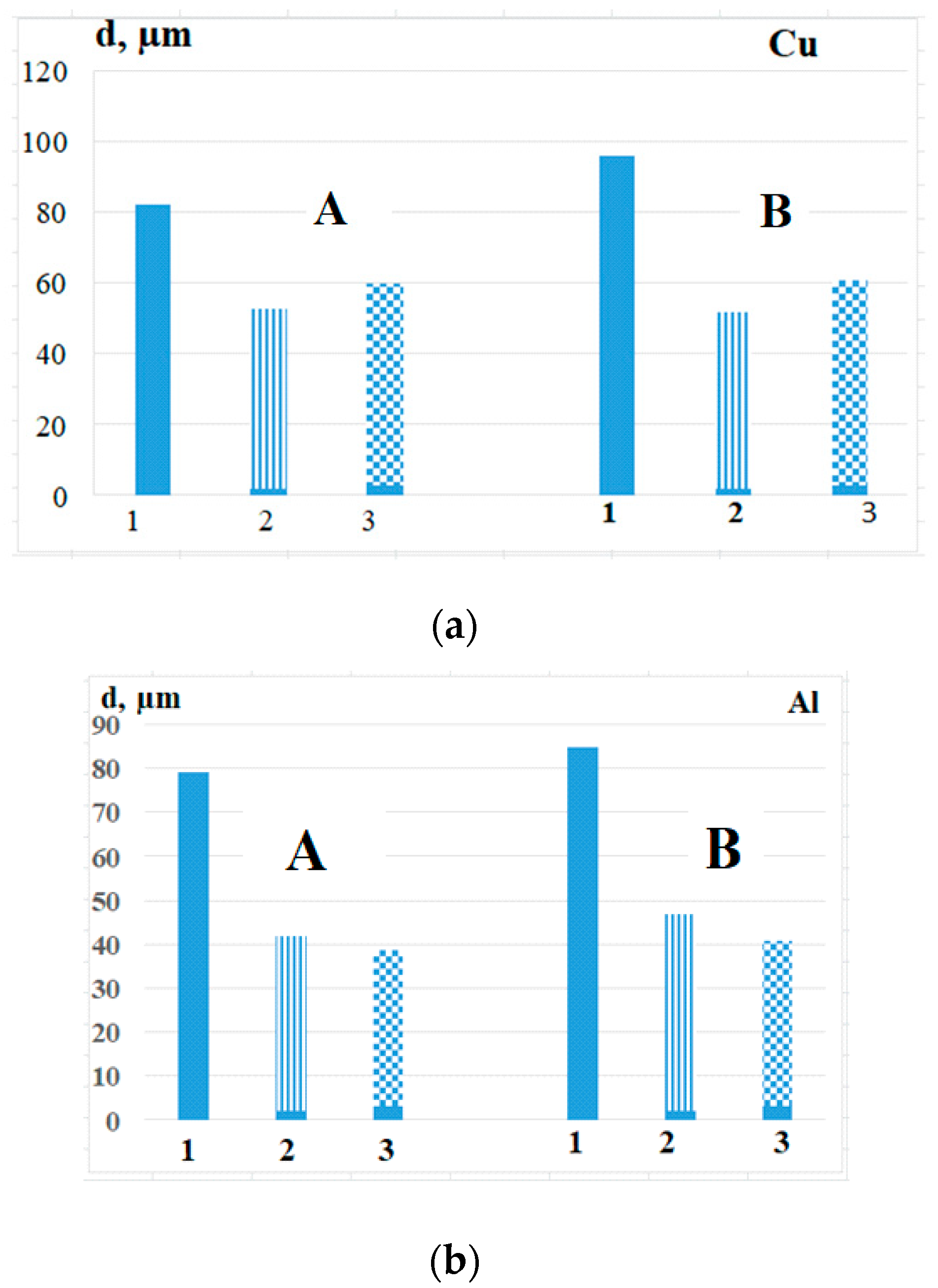
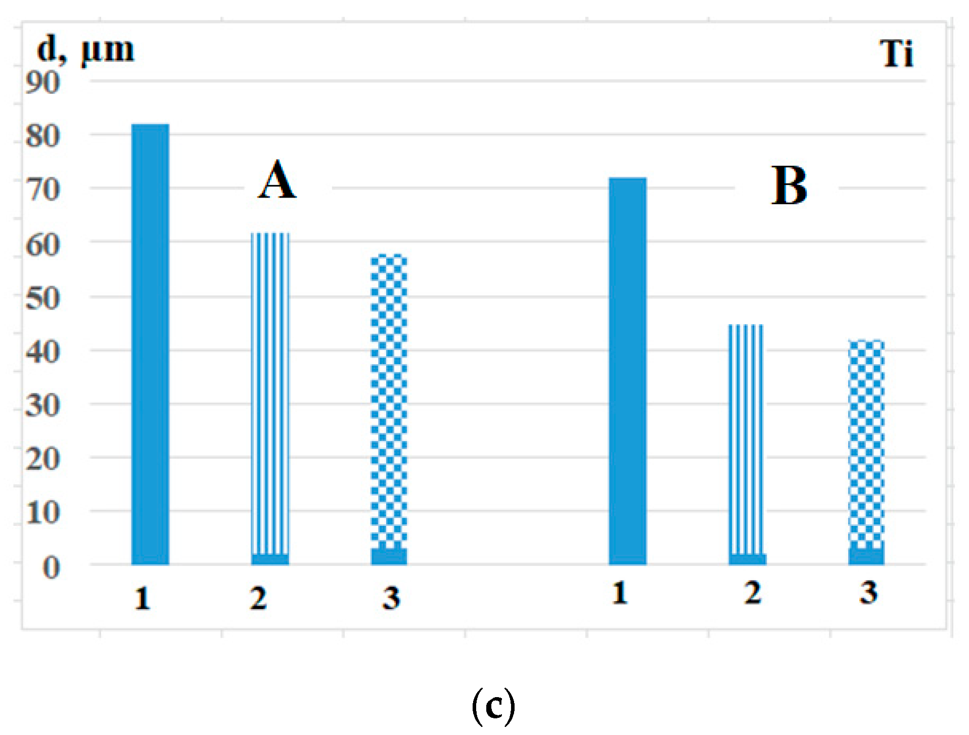
A comparison of the cathode spot diameters determined from the optical images of the front and reverse sides with the measurement of the imprints (autographs) left on the glass surface is shown in
Figure 13 and
Figure 14 for various film thicknesses of copper, aluminum, and titanium. The sample set for the comparative analysis consisted of 10 specimens for which it was possible to reliably correlate image-sequence results with autographs on glass. The results in
Figure 14 are still insufficient for statistical evaluation, and the experimental methodology itself is still being developed. We note only the fact that the minimum cathode spot size obtained from reverse-side imaging is smaller compared to the classical optical investigation methods.
In
Figure 15,
Figure 16 and
Figure 17, the results of reverse-side optical imaging of anode spots are presented for the first time. It can be seen that the internal structure of the anode spot is not as pronounced during image processing. Furthermore, in the optical images (
Figure 15a,
Figure 16 and
Figure 17), the glass surface appears practically clean, without thermal effects that are characteristic of cathode spots. Moreover, in some areas, the film does not evaporate at all and remains intact, as clearly visible in
Figure 17b. The anode spot splits into an elongated ellipsoidal shape, at the center of which the film is distinctly visible. The reverse side of the anode spot appears fragmented in all images in
Figure 15,
Figure 16 and
Figure 17.
In
Figure 18, an optical image of a free cathode spot, first discovered in [
45], is presented. The physical nature of the formation of a free cathode spot is currently unknown. In our experiments, after analyzing more than 50,000 images, 15 images of a free cathode spot were recorded. The cathode spot is located on the clean glass surface, or in some cases borders slightly with the edge of the film.
However, from the optical image in black and white and in color, we see that there is a region in the center where the maximum brightness intensity is present, and the digital matrix of the optical camera becomes oversaturated, producing a black area in the image.
Computer processing of the optical image of the reverse side of cathode spots using Adobe Photoshop C3 makes it possible to process such an image, and the external shape of the free cathode spot, as well as part of its internal structure, becomes visible.
As in works [
43,
44,
45], we note that the cathode spot shown in
Figure 17 is not part of the film material and is not part of the plasma column of the welding arc. According to the classification of cathode spot structure given in [
13,
15,
16,
19,
20,
21,
22,
23,
46], it is located in a spatially free position with respect to them.
4. Discussion
The visualization results of the reverse side of cathode and anode spots presented above demonstrate a completely different approach to studying the phenomenon of cathode and anode spots in the electric arc. It has been experimentally proven that the reverse sides of cathode and anode spots exist in welding arcs (see
Figure 4,
Figure 5,
Figure 6,
Figure 7,
Figure 8,
Figure 9,
Figure 10 and
Figure 11).
In
Figure 4, the dynamics of change in size of the spot and the trajectory of movement are visible. From positions 2 and 3, it is visible how single spots are formed into a group spot of a larger size, position 4. Then we see the chaotic movement of the cathode spot on the film surface. The film under the spot evaporates, and we see a clean glass surface. An important feature of the spot movement is that there are areas of the film under the spot that have not evaporated. This is visible in positions 5, 6, 7, and 8 in the form of a black mark. A similar picture of the unevaporated film in the spot area is observed in
Figure 8,
Figure 15,
Figure 16 and
Figure 17. The brightness of the shooting object changes. If at positions 1, 2, and 3 the brightness was minimal, then it increases at positions 4, 5, 6, and 7. The spot brightness was estimated in most works on cathode spots.
In the work [
13] the author presents a continuous spectrum of brightness over the spot area. In Juttner’s work [
19,
20,
21,
22,
23,
40], it was shown that the brightness intensity in the cathode spot area exhibits an oscillatory nature, indicating a fragmented spot structure. However, the concept of “fragmented” is not equivalent to the concept of a cell. In [
12], a cathode spot cell is defined as an object that allows a minimal current to pass through it. The average values of the number of cathode spots distributed for cathodes of different materials depending on the arc current (
Figure 13) show a direct dependence on the current strength. The obtained data coincide with the results of other authors.
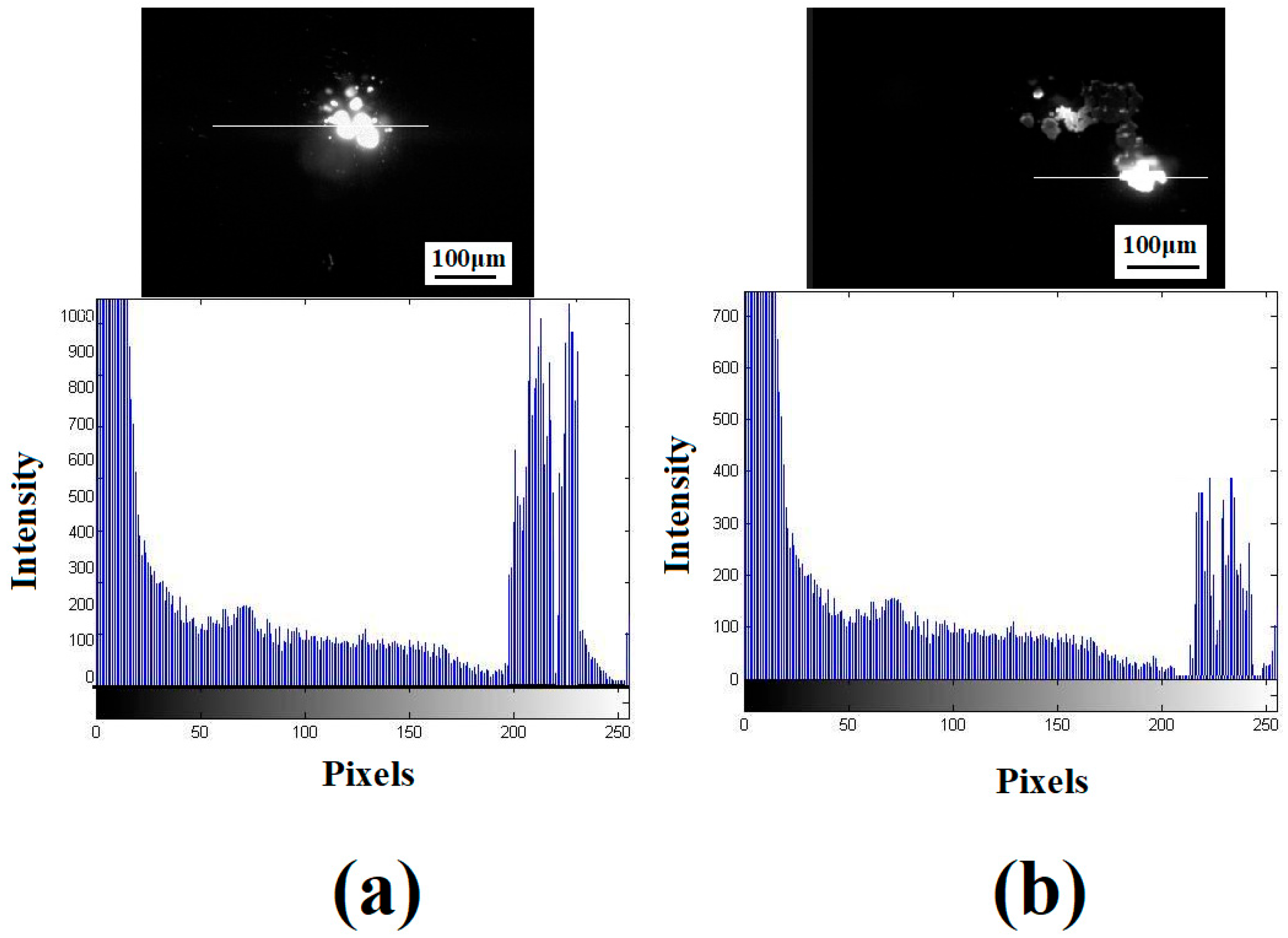
We processed the photographs in Adobe Photoshop C using the brightness and image level features. The results are shown in
Figure 19. It can be seen that, based on the pixel count and brightness intensity measurements in the spot area, an oscillatory brightness spectrum with peaks of maximum and minimum intensity was established within the spot area. This confirms the fragmented nature of the back of the spot. The obtained results correlate with those for the brightness distribution within the spot area during optical imaging of a straight plane, presented in [
19,
20,
21,
22,
23,
30,
40].
Additional processing of the brightness level of the photographs we obtained of the reverse side of the cathode spot in Adobe Photoshop C allowed us to reveal some details in
Figure 20 and
Figure 21.
In
Figure 20a,b, it is clear that adding brightness (top image) yields new details. Near the spot, there are dim brightness zones. Applying brightness level processing reveals additional spots.
Figure 21 presents a completely different picture. In
Figure 21a,b, we see a decrease in brightness over time (frames follow each other sequentially). Further down, at positions (c) and (d), there is just a single dot. Frames (a) and (c) show a single black spot. Adding brightness during processing in Adobe Photoshop C shows that the cathode spot has not faded. The image along the edges of the film is clearly visible. This essentially confirms the hypothesis that the cathode spot has a generation, growth, and division phase, as well as a decay phase, and our proposed shooting method yields qualitatively new information.
Consequently, cathode and anode spots are physical, material objects formed during the burning of the electric arc in gases and possessing at least two-dimensional characteristics in space and time. The presence of a third coordinate for cathode and anode spots—which would immediately raise the question of volume—has not yet been resolved.
General issues of welding arc research methodology. At the same time, the visualization results of anode and cathode spots in a welding arc require separate analysis, considering the novelty of the methodological features of our experiments. Let us focus on the key points needed for the discussion of the results we have obtained, comparing them with those available in the scientific literature.
In the course of analyzing various studies on the theory of cathode spots presented in the introduction to this work, we noted that, in reviewing the current state of research in arc welding, there remain unresolved issues and future directions [
1,
2,
5]. The main attention is devoted to the plasma of the welding arc and its interaction with the electrode and the workpiece during welding with a tungsten electrode in an inert gas environment and with a consumable electrode in an active gas. The areas where further work has been identified as necessary [
1,
2,
5] include the development of methods for measuring the distribution of current density, which is directly related to the cathode and anode spot.
At the same time, we note that most studies in the field of welding are focused on measuring the temperature of the arc. It is evident that such an approach is of limited value for controlling the welding process, since current density is far more important for determining the distribution of heat across the tip of a coated electrode or welding wire and the heat transferred to the workpiece. At present, current density and heat flux have not yet been successfully measured in MIG/MAG arcs, and measurements in TIG arcs require specialized experimental facilities.
However, when calculating current density for welding processes, we assume a solid cross-section of the wire or electrode. However, numerous studies on vacuum arcs indicate that current flows only through the cathode spot; outside the cathode spot, the current tends to zero. A similar situation applies to the heating source of the electrode, the wire, and the weld pool. In welding physics, it is common to consider the metal (the anode) heated through the heating spot across the entire arc column. The presence of cathode and anode spots on the surface of the cathode and weld pool is not taken into account. In our previous work [
43], we demonstrated that anode spots are almost always present on the surface of the weld pool. These spots are the primary sources of metal melting and the maintenance of metal temperature across the entire surface of the molten pool.
Studies [
9,
50] using a high-speed camera (5,000,000 frames per second) show the movement of the cathode spot across the surface of an aluminum weld pool. The authors also found that the presence of cathode spots on the weld pool surface significantly affects surface tension and the Marangoni effect. Because the cathode spot extends outward from the arc center, the pressure is higher in areas where it is present, while in areas without spots, the pressure is lower. This leads to an uneven pressure distribution perpendicular to the surface of the molten pool. This uneven pressure distribution leads to the generation of tangential shear forces. This, in turn, affects the rate of pool solidification and, consequently, the quality of the weld.
Moreover, the temperature distribution in the arc is closely related to the current density distribution through electrical conductivity, so accurate temperature profiles make it possible to calculate the current density distribution. If the boundary region between the arc plasma and the welded workpiece is correctly treated, then a model predicting temperature and current density will also predict the energy transferred to the workpiece during welding.
According to the theoretical concepts currently accepted, during visual observation, the cathode spots appear as very small luminous plasma regions moving along the surface of the cathode.
In the physics of a welding arc [
1,
2,
5], there is currently no theoretical concept for the formation of cathode and anode spots. There is no established experimental basis for studying cathode and anode spots. Results from high-speed camera imaging of cathode spots are primarily presented for aluminum welding. Therefore, we can examine the main concepts and hypotheses for the formation of cathode spots in the vacuum arc region and, based on these, propose our own, taking into account the specifics of welding. The main difference between a welding arc and vacuum arcs is the melting of the metal and its transfer through the arc gap to the weld.
Classification of cathode spots: by geometric dimensions, time of existence, and speed of movement. In theory, a cathode spot represents an arc-shaped region that includes an area of the cathode and a region of dense plasma generation where current continuity is maintained [
12,
13,
14,
15,
16,
17,
18,
19,
20,
21,
22,
23,
24,
25,
26,
27,
28,
29,
30,
31,
36,
37,
38,
39,
40,
41,
42].
In [
16,
46], the author provides the following definition: a cathode spot can be defined as an arc-shaped region that includes the locally heated body of the cathode, while the dense plasma cluster ensures current continuity in the cathode region.
In the works of other authors, cathode processes in the spot are described from the standpoint of the classical sequence: solid body–liquid–evaporation–plasma [
12,
13,
14,
16,
18,
42].
The conditions for evaporation of cathode material in a high-current arc spot were investigated in [
12,
13,
16,
42]. It was shown that in the cathode spot, the evaporation rate of the electrode material depends on the processes that provide the ion flux necessary to maintain thermal and erosive phenomena in the near-cathode region of the arc. Therefore, the vapor outflow is not “free”; it occurs under conditions of high charged-particle density, and its velocity at the outer boundary of the layer may be lower than the speed of sound.
Within this assumption, according to [
14,
19,
20,
21,
24,
25,
26], the formation of high-current group spots or their associations at low external-gas pressure becomes understandable, as well as their transition to individually existing spots as the pressure increases to atmospheric [
13,
14]. It is also possible that the lifetime of the spots is determined not only by the structure of the cathode surface, but also by the time required for the transition to a free-flow regime of the near-cathode plasma.
According to [
14,
42], analysis of these questions—and of the influence of effects related to changes in gas-dynamic parameters along the arc length on the conditions of spot existence—should be carried out on the basis of jointly considering both the processes in the Knudsen layer and in the region of the cathode jet. According to [
12,
13], the concept of a cathode spot unites two physically different regions: the metal surface, which may be heated to the boiling point and above, and the near-cathode region, which forms during the development of the spot. Most researchers of vacuum arcs [
12,
13,
14,
15,
16,
17,
19,
20,
21,
22,
23,
24,
25,
26] understand the term “cathode spot” as small, brightly luminous regions on the cathode surface, which are visually observable and through which the transfer of electric current between the cathode, the arc gap, and the anode takes place [
13,
14].
Classifications of cathode spots are known: by geometric dimensions, by lifetime, by velocity of motion (first-, second-, and third-type spots), and by hierarchical levels [
16,
18,
19,
20,
21,
22,
23,
24,
25,
26,
27,
28,
29]. In accordance with the hierarchy of cathode spots by current and size, a gradation is established based on the characteristic lifetimes of the objects.
In [
16], another classification is given—cathode spots may be divided into two major groups:
In [
17], it is proposed to classify cathode spots according to the modes of their existence, which are determined by the micro-roughness parameters of the cathode surface and by structural factors of the material.
Modern high-speed visualization makes it possible to determine spot behavior under the influence of external gas pressure, magnetic-field action, cathode geometry, preliminary cathode treatment, and current rise rate. Using this methodology, most authors observe various types of local brightness regions, referred to as cathode spots, depending on the listed conditions. In general, they differ in velocity, number, local-spot current, and lifetime.
Thus, the dynamics of the various types of spots described in the scientific literature and their classification (with numbering in Arabic numerals (1, 2, 3…) or Roman numerals) is based on a single experimental fact—the optical brightness of regions on the cathode surface and the velocity of motion of these bright regions. The optical brightness of these regions is obtained when imaging from the front side of the cathode and, therefore, as we indicated in
Figure 2, is nothing more than the plasma jet ejected by the cathode spot, i.e., a plasma cloud rather than the spot itself.
As a result, all experimental studies using high-speed optical imaging of cathode spots [
12,
13,
14,
15,
16,
17,
18,
19,
20,
21,
22,
23] are effectively studies of the plasma cloud above the spot. This is not primary and not even secondary radiation—it is most likely additive radiation. The structure of the spot is not determined in such observations.
The further classification proposed in [
46] based on spot parameters—velocity v
sp, spot current Is, lifetime t
s and their location, as well as the condition of the cathode surface—is not entirely correct, since the object of classification is unclear. Although the author proposes that spots can be identified directly through parameters characterizing their external appearance, for example:
- –
Very fast-moving spots (SFS) on surfaces with impurities, oxides, or roughness;
- –
Moderately fast-moving spots (MFS) on cleaned and smooth surfaces;
- –
Film cathodes (FiS)—metallic films on glass or metals;
- –
Slowly moving independent spots (SIS);
- –
Group spots (GS), which are associations of sub-spots, fragments, or cells.
Some spot types depend on the interelectrode gap length or on natural/applied magnetic fields. However, the most fundamental issue—the external appearance of cathode spots, which forms the basis of this classification—has not been experimentally established.
In our experiments [
7,
43,
44,
45] and in the works of other authors [
3,
9,
10,
11], two or three types of cathode spots have been recorded so far:
- –
Very fast-moving spots (SFS) on surfaces with impurities, oxides, or roughness [
3,
7,
43,
44,
45];
- –
Moderately fast-moving spots (MFS) on cleaned and smooth surfaces [
9,
10,
43,
44,
45];
- –
Film cathodes (FiS)—metallic films on glass or metals [
44,
45];
- –
Slowly moving independent spots (SIS) [
7,
8];
- –
Group spots (GS), which are associations of sub-spots, fragments, or cells [
7,
8,
9,
10,
11].
A large series of experimental studies [
16,
19,
20,
21,
22,
23,
24,
25,
26] provides a different classification. The terms “Macrospot”, “Spot”, and “Cell” differ in the level of passing current and size. A “Macrospot” spot is an association of several “Spot” spots. The “Spot” spot itself consists of “Cells”. For copper, the characteristic dimensions of a “Macrospot” are (1–3) · 10
−2 cm, for a “Spot”, (1–2) · 10
−3 cm, and for a “Cell”, <5 · 10
−4 cm. In [
19,
20,
21,
22,
23,
24,
25,
26], it is also indicated that “Macrospots” can also form associations called “Group Spots”.
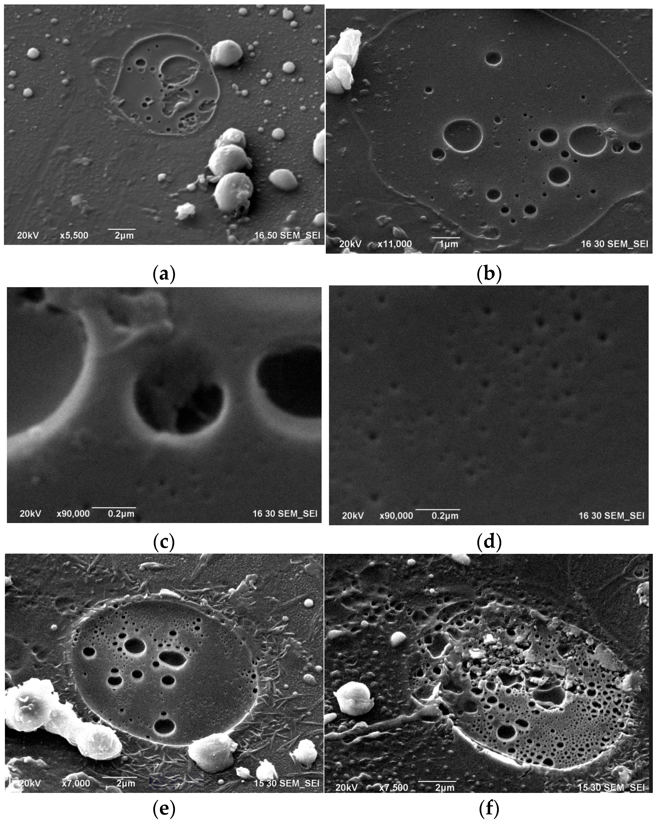
Thus, the important parameters of a spot are its geometric size, which is used to calculate the current density in the arc. In our experiments, we obtained imprints of the reverse side of the cathode spot (
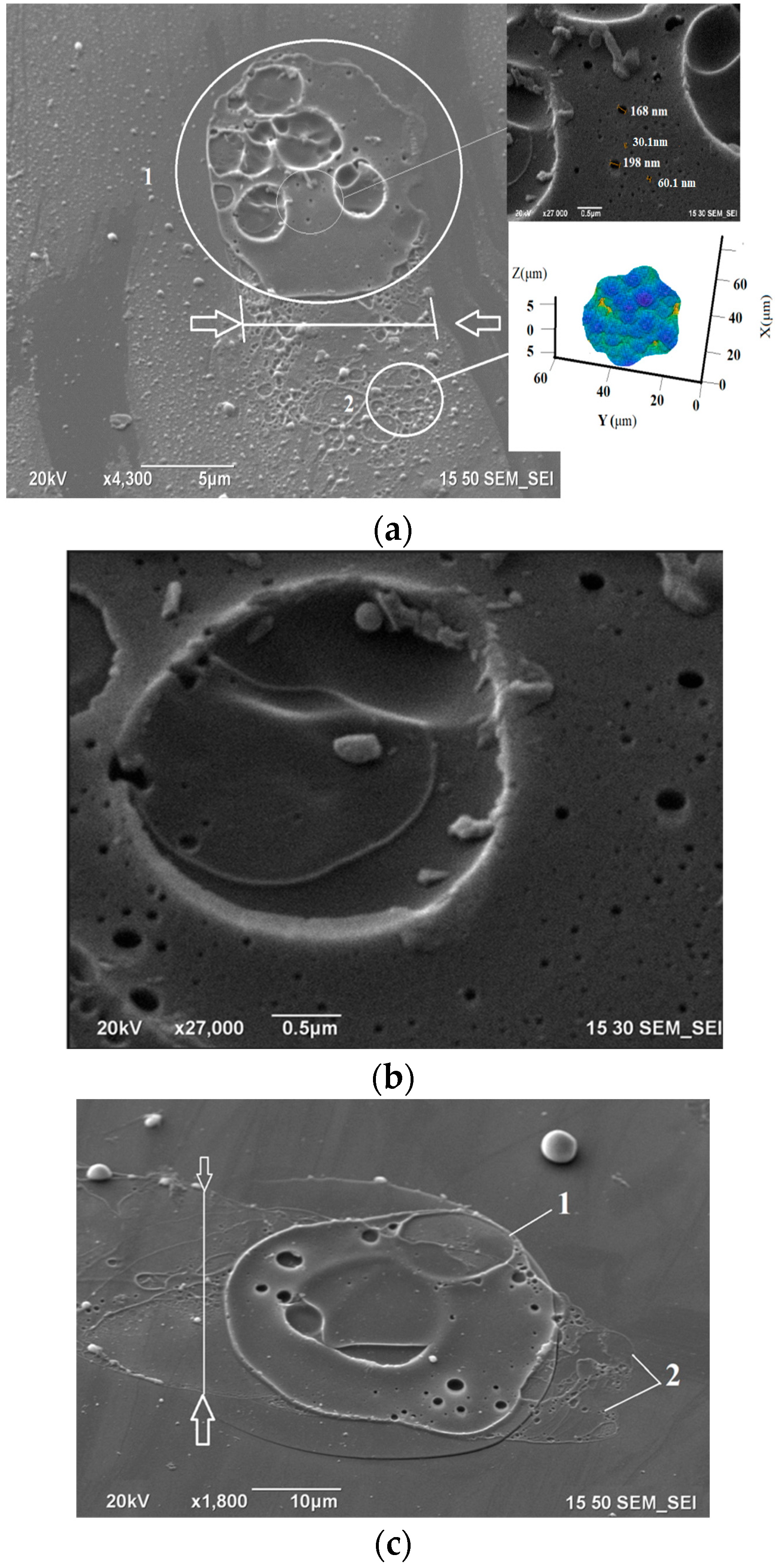
Figure 22). It is difficult to determine the true current density from these imprints, as it is not entirely clear what to take as the basis. Is it the outer diameter of the cathode spot, or the fragmented portion within the spot area, or should these values be summed? If we examine the imprint surface carefully using a high-resolution electron microscope, we see crater sizes ranging from 15 nm to 80 µm (
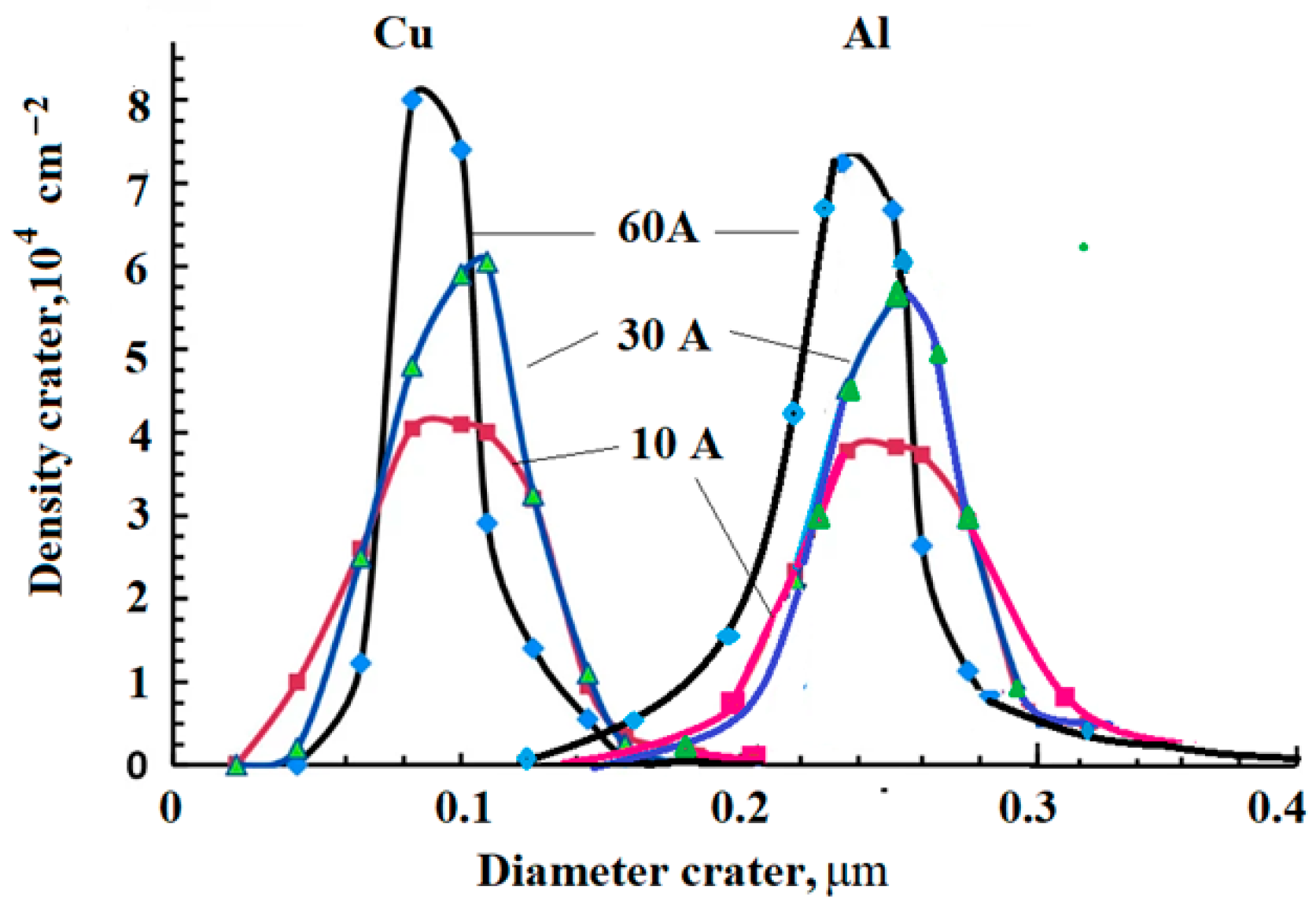
Figure 22c, d). The outer boundaries of the cathode spot backside imprints are nearly circular. The internal fragments are represented by round holes of varying diameters. The density of internal fragments was calculated for two materials, copper and aluminum (
Figure 23). For each material, 30 samples were examined under an electron microscope at various magnifications. It is clear that for copper, the diameter sizes are in the nanometer range, with μm not exceeding 0.1–0.2 μm. For aluminum, the range is slightly higher, with the minimum fragment diameter in the range of 0.15 μm and the main diameter 0.2–0.3 μm. Clearly, such fragments of the cathodic spot will exhibit high current densities.
The work [
14,
46] proposed spot models in which the simultaneous presence of two current density values during the spot’s lifetime was assumed to satisfy various spot processes and observed parameters. The author assumed the presence of two current density values, which were specified arbitrarily. On the one hand, he assumed that to satisfy the cathode energy balance, a relatively large cathode spot with an average current density of 10
5 A/cm
2 should form on the cathode. On the other hand, this spot consists of many small spots, randomly moving with a current density of 10
7 A/cm
2, which made it possible to describe the mechanism of cathode electron F-emission.
The presented results on the measurement of crater density agree qualitatively with the results of [
41,
42]. In this work, signatures on the surface of a copper cathode were examined using an electron microscope. Later, in the work of other authors [
52], data were presented on other materials, and the crater densities were calculated depending on the current strength. Our data on the distribution density of craters in signatures on the back side of the cathode spot and their sizes are in good agreement with the results of these works. Taking into account the results we have obtained, further information is needed on the size of craters in relation to volumetric cathodes, the distribution of craters, and the lifetime, depending on the welding method and the material being welded.
An important experimental fact was the detailing of the backside signature of the cathode spot and track (
Figure 24). A detailed examination of the cathode spot signature, including fragment measurements within the spot area and surface roughness measurements of the track, revealed not only a large number of small craters measuring 0.12–60 nm within the spot area, but also the inner surface of larger craters.
Figure 24a shows fragments of the smallest craters, along with the track and measured roughness.
Figure 24b shows small fragments measuring nm.
Figure 24c shows a surprising fact, shown by numbers 1 and 2. Number 2 shows the spots at the moment of movement; they are smaller. Number 1 shows the moment the spot returns to a steady state.
Measuring the roughness parameters of the cathode spot trace reveals a wavy surface with peaks and valleys. Clearly, as it moves, the cathode spot oscillates along the (x, y, z) axes across its area. This was a new property of the cathode spot, which we were able to detect using our method. It is possible that the cathode spot has three dimensions and, due to internal fragmentation, is in continuous oscillatory motion along (x, y, z) space and time.
Phenomenological description of the physical essence of cathode spots as a new property of electric current. The results of our study presented in
Figure 13 and
Figure 14 confirm this fact by showing comparative histograms of the ratios between the cathode-spot diameters measured from the front side, the reverse side, and the thermal imprint on the glass. Our study presents experimental evidence of the actual appearance of cathode spots. The spot diameters measured optically from the front side are larger—not by percentages but by multiples—compared with those measured from the reverse side (in our experiments).
In our work we also deal with light of varying intensity, but in our method the light originates directly from the cathode spot. When we process this radiation, we obtain the true internal structure of the light-emitting sources located within the spot itself. Based on this experimental fact, all our conclusions about fragments, cells, and substructures within the spot area are correct and reliable, as they are based on the primary optical signature recorded by the high-speed camera.
The second distinguishing feature is the autograph left by the reverse side of the cathode spot on the glass surface, which correlates with the optical measurement.
There are clear differences in the visualization of the cathode and anode spots from the reverse side. This is clearly visible in
Figure 10 and
Figure 12 (cathode spots) and
Figure 14,
Figure 15 and
Figure 16 (anode spots). This is clearly visible in
Figure 8,
Figure 9,
Figure 10 and
Figure 11 (cathode spots) and
Figure 14,
Figure 15 and
Figure 16 (anode spots). Cathode spots have a structure within the spot area. In the optical image, this structure is fragmented. The structure lacks a clear geometric shape. However, the signature left by the cathode spot on the glass has a clear structure in the form of multiple circles (
Figure 7).
Since there is no theory of the formation of the cathode and anode spots in welding arcs in the physics of welding arcs, let us turn to an analysis of work on vacuum arcs.
Let us first briefly formulate the experimental facts. Cathode spots are centers of electron emission. Electrons leave the metal not as a general flow, but in the form of current channels [
44]. Changes in brightness values during visualization of cathode spots were noted in the works of Juttner and others [
12,
13,
14,
15,
16,
17,
18,
19,
20,
21,
22,
23,
24,
25,
26,
27,
41,
42,
46,
53,
54,
55,
56,
57,
58]. This served as an argument for cathode spot fragmentation.
There are numerous studies on visualizing cathode spots in the lifetime range of 10 ns to 1 s, with spot sizes ranging from 0.1 to 100 μm. However, these facts are not taken into account in theory.
The first group of theories is the stationary gas-dynamic theory of the cathode spot. The authors postulate that the cathode spot already exists. How it formed is unimportant. Its size is unimportant. Issues of cathode spot division and fragmentation are unimportant. What happens on the metal surface and in the surface layer is unimportant, since the cathode material melts and evaporates.
The second group of theories is the explosive emission mechanism. The authors postulate that there are inhomogeneities and defects on the cathode surface.
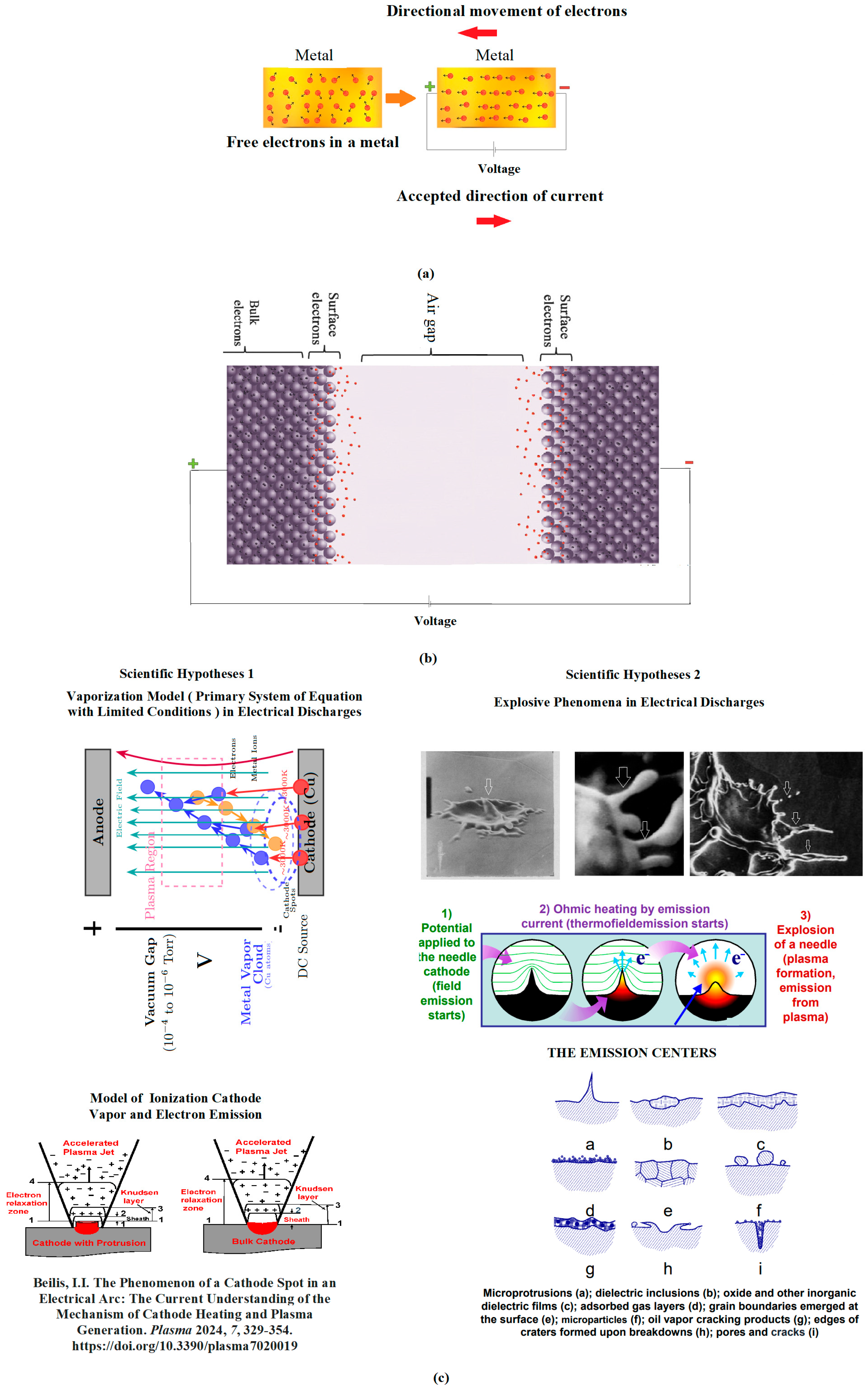
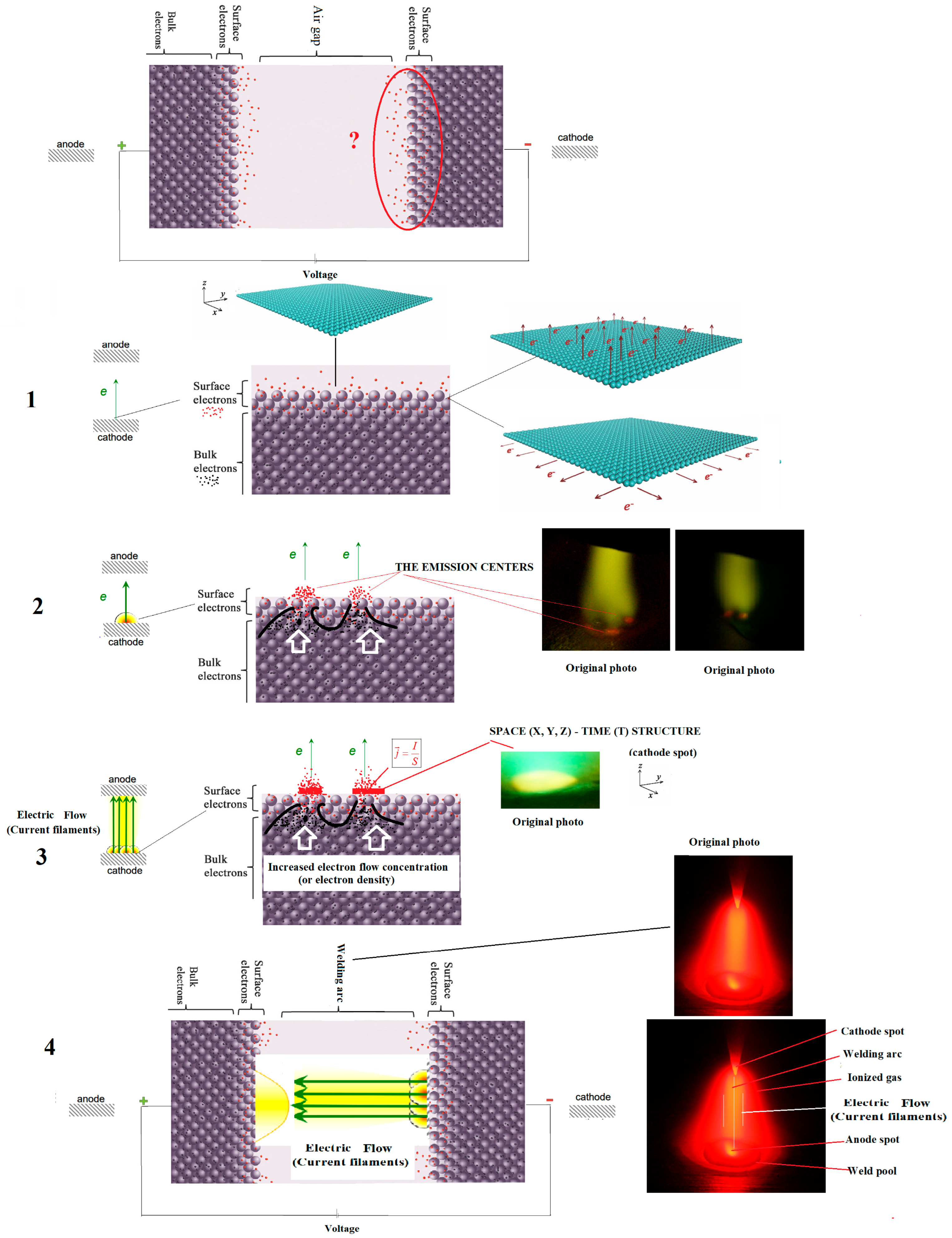
Figure 25 schematically shows two groups of theories devoted to the mechanism of cathode spot formation.
Figure 25a presents the classical knowledge about electric current in metals.
Figure 25b shows the metal–dielectric–metal diagram.
Figure 25c explains how an arc discharge occurs through a cathode spot.
The paper [
53] demonstrated that the field emission current arises from a number of individual localized emission points on the cathode. These spots were shown to be protrusions in the form of filamentary structures on the cathode surface, where the electric field is significantly enhanced. The DF emission model suggests explosive evaporation and emission of electrons from various protrusions caused by Joule heating. This process occurred over the lifetime of the spot due to numerous protrusions over a large cathode area.
In [
15,
27,
28], the very concept of the cathode spot is replaced by a new, undefined term, “active emission centers,” introduced by the author within the framework of the ecton mechanism of vacuum-arc operation. According to the author [
7,
20,
21], an ecton is formed through the interaction of a jet of molten metal with plasma. When the current exceeds a threshold value, the jet of liquid metal forms a droplet. This droplet, even before detachment, leads to an increase in the ion current density from the plasma at the junction between the jet and the droplet. This results in a higher concentration of energy at the junction and in the initiation of an ecton (explosion) due to Joule heating of the junction.
In view of the above, neither the author [
15] nor their colleagues have ever experimentally demonstrated what this object defined by the vague term “active emission center” actually looks like (optically or via the autograph method) on metal.
The argumentation proposed by the author [
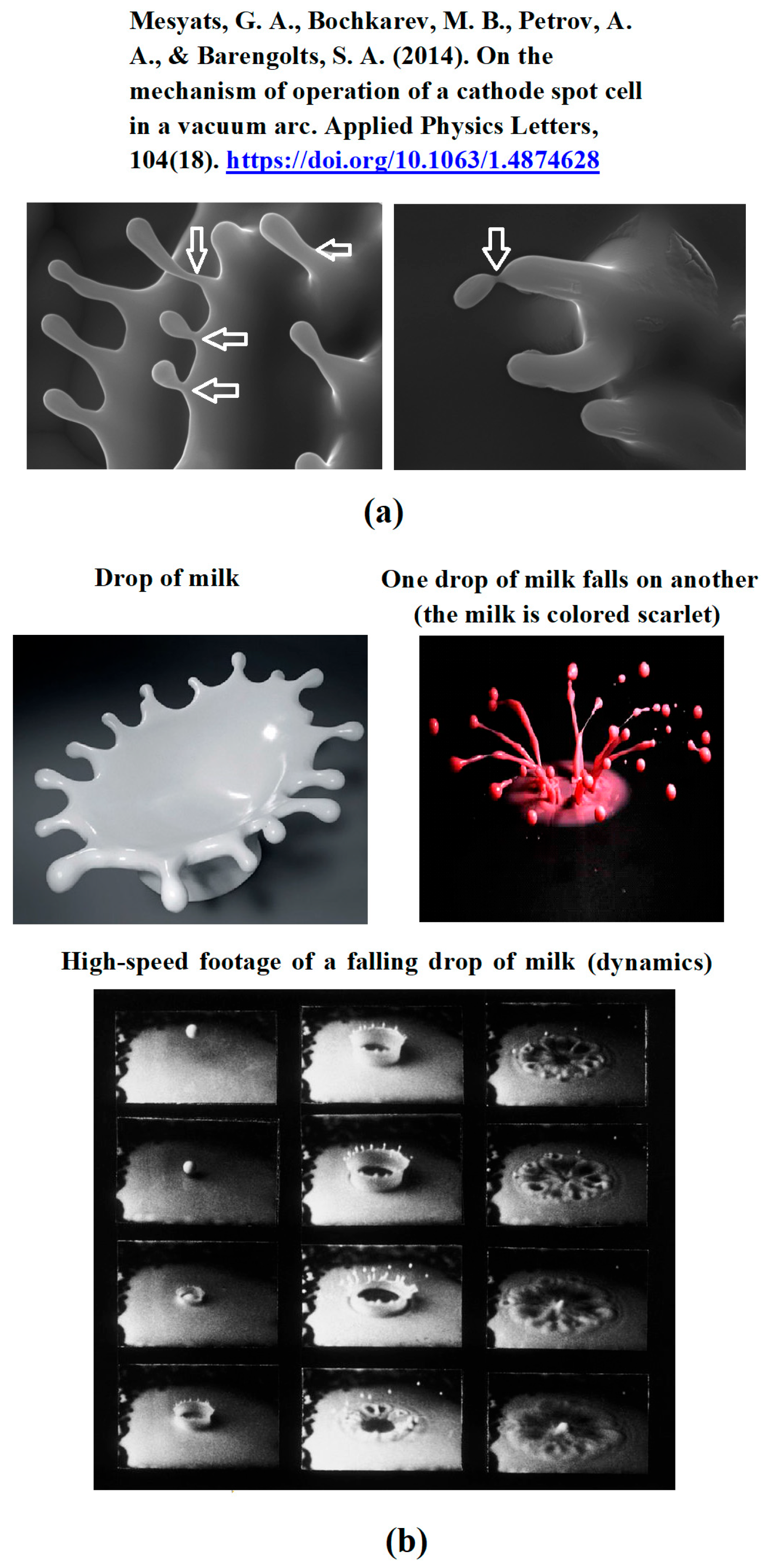
15] regarding the formation mechanism of the cathode spot in the form of frozen droplets evokes the implication that a similar phenomenon already exists. Similar photographs are virtually identical to high-speed images of milk droplets, where analogous splash structures form upon impact with the surface. For example, on the internet, one may easily find numerous original photographs of falling milk droplets that look almost identical to the images used by the author of [
15], yet such structures form without the need for high energy concentration at the junction or involvement of an explosive effect (
Figure 26).
The introduction of the new concept of the cathode spot in the form of an undefined term—“active emission centers”—and the attribution of specific properties to it [
15], and subsequently the drawing of far-reaching physical conclusions about all processes in the arc discharge based on a single mechanism of explosive emission, appear incorrect and premature. An important fact: proponents of explosive emission and the new concept of the cathode spot have not provided a visual representation of what this spot looks like [
15,
27,
28,
29,
32]. There is not a single study where authors have recorded these “active emission centers” using optical methods.
The author of [
15] ignored the critical theoretical comments presented in [
13,
14,
16,
46], where it is stated that such a mechanism has a limited, local domain of existence for micro-inhomogeneities on the cathode surface with protrusion heights of 10
−7–10
−8 cm and voltages exceeding 200 V. For vacuum arcs and even more so for welding arcs, where the cathode voltage drop is, for copper, 14.7–15.4 V; titanium—10.5–11.5 V; iron—17.1–18.0 V; and tungsten—16.2–22.6 V. For film cathodes, where the drop is, for copper, 11.2 V; aluminum, 4.2 V; and titanium, 4.0 V [
1,
46], this mechanism of explosive electron emission is entirely impossible [
1]. The limited applicability of explosive-emission phenomena in cathode spots of vacuum arcs is noted in [
16,
18,
19,
20,
21,
22,
23,
24,
25,
26].
Thus, it is important to distinguish spots by their different shapes and internal structures so that the mechanism can subsequently be studied with consideration of the general properties obtained experimentally. The visualization method of the reverse side of cathode and anode spots proposed by us makes this possible.
Figure 10 shows the fragmented reverse side of the cathode spots over time for a current of 30 A and a copper film thickness of 68 nm—the formation of a cathode spot occurs every 0.005 s. Using image processing software with brightness gradient filters allows us to distinguish the structure of the cathode spot (see
Figure 4,
Figure 5,
Figure 6,
Figure 7,
Figure 8 and
Figure 9). A comparison of different methods for photographing the cathode spot in
Figure 13 shows that the diameters of the spots on the reverse side are smaller than those on the front side.
For further investigation of the mechanism of cathode-spot formation in welding arcs, new approaches are required to explore the essence of the phenomenon, whose basis is the electric current. The hypothesis proposed by the author of [
44,
45]—that cathode spots represent a new, previously unknown property of electric current—is admissible and does not contradict existing scientific principles; rather, it complements and develops them. All of this is related to the modification of the fundamental properties of electric current at the surface. These changes are primarily “regulated” by the amount of electric charge dI passing per unit time through the entire surface dS of the cathode (the current), by the amount of electric charge dI passing per unit time through an arbitrarily oriented surface element dS (the current density within the cathode-spot area), and by the thermophysical properties at the cathode surface. The quantity dI is determined by the volume charge density and by the charge drift velocity.
It is well known that the flow of electric charge can be controlled by increasing the current frequency, causing it to concentrate in the near-surface layer (the skin effect). In our case, there also exists an experimental fact [
12,
13,
14,
16,
18,
19,
20,
21,
22,
23,
24,
25,
26,
27,
28]: when cathode spots form on the cathode surface, the entire electric current flows through them, while outside the spot area, the current values are close to zero. Thus, we see that the flow of electric charge can indeed be controlled. Moreover, it is precisely the cathode spots that provide the high current density in an arc discharge, which by analogy resembles the phenomenon of superconductivity in metals [
59,
60].
The fact that the flow of electric charge can be controlled, and that the carriers of superconducting current are electron pairs, suggests that we must search for the mechanism that binds electrons into pairs in the thin surface layer of the cathode metal. Why? Presumably, it is precisely the electron flow in the surface layer that becomes localized in the region of the cathode spots in order to provide the high current density of emitted electrons. If the electron flow becomes localized in a point-like object, then there must exist a mechanism of such localization; therefore, the process of cathode-spot formation is an expression of a new property of electric currents.
Currently, a wide range of models of welding arc columns has been developed, describing it from various points of view and with varying degrees of detail. Models reflecting physical processes include: the channel model of the arc column [
2], the cylindrical model of the arc column [
2], the two-temperature model of the welding arc column [
2], the vortex electrodynamic model [
61,
62], the thermal model, etc. [
1,
2].
We propose a qualitative hypothesis of the mechanism of formation of the cathode spot in a welding arc exclusively from the point of view of electrical theory (
Figure 27). Having analyzed the results of the works of various authors, we generalized these results [
1,
2,
12,
13,
14,
15,
16,
17,
18,
19,
20,
21,
22,
24,
25,
26,
27,
46,
61,
62,
63,
64] based on our experimental data [
7,
8,
43,
44,
45,
51,
52].
Consider the option of bringing the electrodes closer together, as occurs during manual arc welding. The cathode surface, as applied to welding, consists of numerous microroughnesses. When voltage is applied from the power source, an electric field E is generated in the interelectrode gap. As the electrodes approach each other in the arc gap, the electric field strength will increase [
2]. When the electric field strength during arc initiation reaches approximately 10
6–10
8 V/cm [
12,
13,
14,
15], field emission will occur from the protrusions of the microroughnesses—the cathode’s conduction electrons will begin an ordered, directed motion and will “flow” from the tip of the microroughness.
Conductors obey the principle of electrical neutrality: in the absence of electric current, charges are distributed only on the surface of the conductor. Within the bulk of the electrode metal, the electric field is zero. Consequently, as electrons leave the tip, a localized, uncompensated positive charge will develop in the protrusion region, resulting in a localized electric field. Under the influence of this field, electrons from the near-surface zone of the cathode will begin to move. They will move along the field lines to compensate for the excess positive charge of the protrusion. As a result, a dynamic equilibrium is established between the outflow of electrons from the solid and their inflow from the bulk of the solid, i.e., a current will flow through the microtip. A localized electron flow will arise on the surface and in the surface layer of the metal. Electron flow concentration is a physical quantity that determines the density of free electrons in a material, plasma, or beam, expressed as the number of particles per unit volume (m−3 or cm−3). Metals have a high concentration of free electrons ((1023)–(1029) m−3), which is virtually independent of temperature. Field emission begins. Moreover, in the cathode–air gap–anode system, only in the solid state are there electrons in large quantities.
This current causes Joule heating of the cathode’s metal microroughness, melting and evaporation of the microprotrusions, and the formation of craters on the cathode’s surface. The localization of electron flows on the surface of the cathode increases the temperature and causes a strong glow, which we see visually in the form of separate cathode spots.
Electrical conductivity reflects the concentration and mobility of charge carriers in the plasma. In the region of the cathode surface and the discharge gap, where ionization is enhanced, the conductivity at the peak of the electric field increases significantly, with the maximum conductivity exceeding 8 × 10
3 S/m [
1,
2]. This leads to the formation of an effective conductive channel inside the discharge gap. As the electric field strength increases, the degree of gas ionization also increases, and the conductivity changes proportionally to the electric field strength. According to Ampere’s law, the interaction of the electric and magnetic fields generates a circular magnetic field around the plasma channel under the influence of strong currents. In turn, the magnetic field also affects the plasma channel. Since the current density is most concentrated at the emission center of the cathode spot, and the magnetic field intensity is highest on the electrode surface, this explains why we observe brightly glowing areas of nearly circular shape in experiments, as well as imprints left on the cathode surface. Thus, an electron-conductive cord is formed in the gas gap, which closes the current circuit of the welding arc column between the cathode and anode. The electron-conductive cord has a negative volume charge, meaning it will attract positively charged particles—ions—formed as a result of ionization of the interelectrode gap during arc initiation. Thus, when the electric arc is initiated, field emission causes the microroughness of the cathode to become emission centers through which the main discharge current flows. As a result, a cathode spot forms on the cathode surface—a collection of fragmented centers. This highly heated region, measuring 10
−3 to 10
−4 cm in size, has a current density of 10
−6 to 10
−8 A/cm
2 and is adjacent to a brightly glowing plasma composed entirely or partially of the cathode material. As the arc burns longer, the entire cathode surface heats up and melts, and thermal field emission of electrons begins. Higher current density leads to greater Joule heating, significantly increasing the temperature of the arc column in the cathode spot as the discharge current increases. Joule heating, generated by the electric current between the anode and cathode, is the primary source of thermal energy in arc welding.
The high-quality model we presented for cathode spot formation and welding arc generation does not contradict the fundamental laws of electricity and is based strictly on repeatedly verified experimental facts regarding cathode spot visualization. High temperatures and explosive emissions are not required to explain the mechanism of cathode spot formation; everything needed is already available in electrical theory. The main events occur in the surface layer of the metal and on the surface of the cathode, and are associated with the flow of electrons in the solid, which is localized.
We explained everything from the perspective of electrical theory, so let us reiterate that a welding arc, or vacuum arc, is an electric arc and obeys the fundamental laws of electricity. Clearly, the formation of cathode and anode spots on the surface of solids for the “solid body-gas gap-solid body” system is a new property of electric current [
44,
45].
This determines, in space and time, the mechanism of electron emission from the surface of a solid (liquid, or mixed-state) body, the dominance of one mechanism over another, the sequential replacement or simultaneous existence of several emission mechanisms, and so forth.
Plasma processes in the near-cathode region are important, but they are secondary, since the primary processes are the fundamental processes of current flow at the surface and in the surface layer of the cathode. The term “structure of the cathode spot” does not fully reflect its physical nature; probably, if we are speaking about the amount of electric charge dI, it is more correct to introduce the concept of the energy state of the cathode spot.
Thus, the material presented demonstrates the results of a newly developed experimental method for studying the reverse side of cathode and anode spots. At present, the available experimental data are insufficient for obtaining analytical dependencies, and we will endeavor to present such results in future publications.
In the future, we plan to refine the data processing methodology and switch from black-and-white to color imaging. Considering that the images presented in this work were extracted from videos with a 1 ms interval and that the processes of merging and dividing the cathode spot are stochastic in nature, it is important to select an appropriate interval to clearly display the characteristics of cathode spot movement. It is possible to extract 1500, 750, 600, 300, and 150 images from a 1–2 s video, maintaining the exposure time at 0.05 ms. Additional intervals of 2 ms, 4 ms, 5 ms, 10 ms, and 20 ms, which were compared with the 1 ms interval, should be optimized. Future research should consider using other cathode materials, such as steel; develop a new method for applying film cathodes; and try other welding methods.





 ,
,