Article

Capacitive-Loaded High-Power Low-Loss 3.0 T Magnetic Resonance Imaging Radio Frequency Combiner Design and Integrated Application

School of Biological Science and Medical Engineering, Southeast University, Nanjing 210000, China
*
Author to whom correspondence should be addressed.
Appl. Sci. 2025, 15(11), 5940; https://doi.org/10.3390/app15115940
Submission received: 30 March 2025 / Revised: 3 May 2025 / Accepted: 20 May 2025 / Published: 25 May 2025
(This article belongs to the Special Issue Advanced RF/MM-Wave Circuits Design and Applications)

Abstract

For high-power magnetic resonance imaging (MRI) radio frequency (RF) combiners operating in the frequency range from 60 MHz to 300 MHz, the primary challenges lie in achieving high-power transmission capability while minimizing the insertion loss (IL), reducing the physical dimensions, and meeting application bandwidth requirements. This paper presents a high-performance RF power combiner based on capacitor-loaded microstrip technology for 3.0T MRI radio frequency power amplifier (RFPA) systems. The proposed combiner features low loss, high integration, and miniaturization, and it comprises multiple branches, each employing microstrip lines and capacitors in a series–parallel arrangement to achieve an impedance transformation of 50 Ω to 100 Ω. Each branch was designed through theoretical analysis and electromagnetic simulations to achieve a line length 30% shorter than λ/4, a 6.2 mm line width, and 0.08 dB IL at the 3.0T MRI operation frequency band. A two-way to one-way combiner was further designed using this branch structure to achieve 0.2 dB IL through simulation optimization. A four-way to one-way combiner was then constructed by cascading two-way combiners and optimized via ADS-HFSS software(ADS2014 HFSS19) co-simulation. The fabricated combiner module uses an FR4 substrate and achieves a 0.4 dB insertion loss, −25 dB return loss, and 25 dB port isolation at 128 MHz ± 1 MHz, with compact dimensions (320 × 200 × 10 mm). To ensure high power capability, thermal analysis was performed to confirm that the module’s power-handling capacity exceeded 8 kW, and experimental validation with the 8 kW 3.0T RFPA demonstrated a stable temperature rise of approximately 2 °C. In this study, the innovative single-branch topology and the RF high-power four-to-one combiner for 3.0T MRI systems were used, resolving the trade-offs between power-handling capability, insertion loss, structural compactness, and operating bandwidth in MRI power combiners. The combiner was successfully integrated into the 3.0T MRI RFPA system, reducing the overall dimensions of the RFPA system and simplifying its installation, thereby enabling high-quality imaging validation. This solution demonstrates the scalable potential of the design for other high-field MRI systems operating in the MHz range (from tens to hundreds of MHz), including in 1.5T and 7.0T MRI systems.

1. Introduction

In ultra-high-field magnetic resonance imaging (MRI) systems, radio frequency (RF) power combiners serve as critical components between RF coils and RF power amplifiers, with their core elements including transmission lines, inductors, and capacitors [1]. These combiners must exhibit exceptional power-handling capabilities: 1.5T MRI RF power amplifier (RFPA) systems require combiners to withstand pulse powers exceeding 20 kW, while 3.0T systems demand handling capacities of up to 40 kW [2]. Consequently, the key components in high-power MRI combiners must endure large currents and high voltages, resulting in increased physical dimensions and elevated losses. Current mainstream solutions widely adopt microstrip lines or lumped-element components combined with Wilkinson structures [3], yet they face persistent challenges, such as excessive size, high losses, poor parameter consistency, and difficulties in integrating with printed circuit boards (PCBs). For instance, in 3.0T MRI systems, a conventional one-quarter-wavelength microstrip line segment measures 0.6 m, and a four-way combiner requires six such segments totaling 2.4 m [4]. This not only leads to volumetric expansion but also exacerbates conductor losses due to increased line resistance. On the other hand, lumped-element solutions, while reducing size, necessitate high-current-tolerant inductors—typically implemented as air-core or magnetic-core structures—which suffer from complex fabrication processes and persistent size constraints [5].
The existing research has predominantly focused on bridge configurations and Wilkinson structures, with the former commonly used in RF coils and the latter in RFPA [6]. However, the operating frequency of the MRI system ranges from tens to hundreds of MHz and meets the requirements of high-power output [7]. The microstrip-based implementation method has a large size and high loss due to the long line length, making it difficult to meet power capacity requirements. The lumped component method faces challenges such as discrete circuit parameters and difficulty in the heat dissipation of various devices. In the traditional design of combiners based on λ/4 microstrip transmission structures, conductor loss and dielectric loss can be effectively reduced by, respectively, increasing the line width of the microstrip and selecting low-loss dielectric materials. However, in high-power, MHz-range (from tens to hundreds of MHz) MRI applications, the quarter-wavelength (λ/4) microstrip lines exhibit excessive physical length, leading to oversized dimensions and significant conductor losses [8]. For lumped-parameter combiners, enlarging the wire diameter of inductors introduces similar challenges [9]—increased size, elevated thermal dissipation, and inconsistent inductance values—all of which degrade combiner performance.
Reference [10] achieved low-loss coaxial combiners under high-bandwidth conditions, but this method remained confined to narrowband, low-power scenarios and is ineffective for MRI systems. Reference [11] proposed a lumped-element model and tuning technique for narrowband RF combiners, reducing impedance distortion and achieving ultra-high efficiency (13.56 MHz, 1 kW); however, its reliance on ferrite cores introduced consistency challenges and severe heating-induced nonlinearities at 3.0T MRI frequencies. Reference [12] underscored the critical need for compact, low-loss multi-channel RF combiners in 7.0T systems employing parallel transmission (pTX) technology, emphasizing the growing demand for miniaturization and efficiency in ultra-high-field MRI environments, and the proposed design demonstrated superior performance in this scenario, achieving both loss reduction and compact multi-channel integration that enhances clinical system practicality.
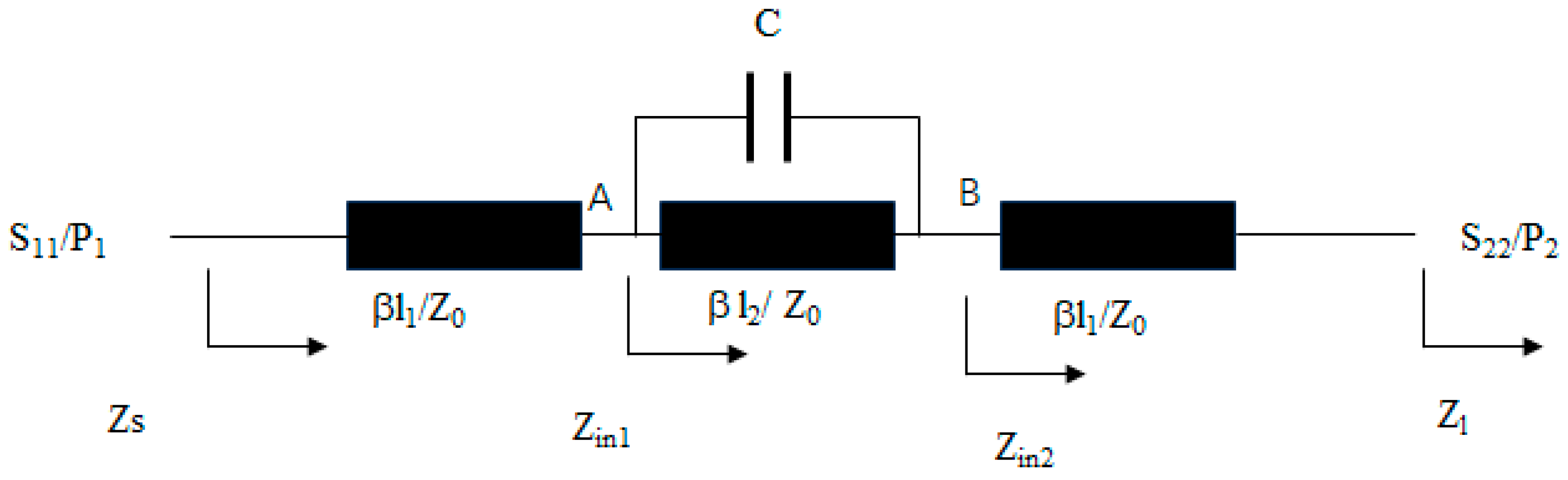
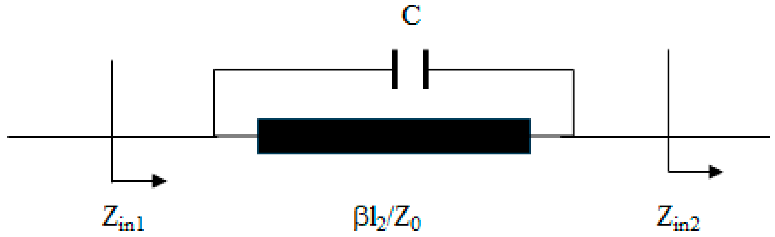
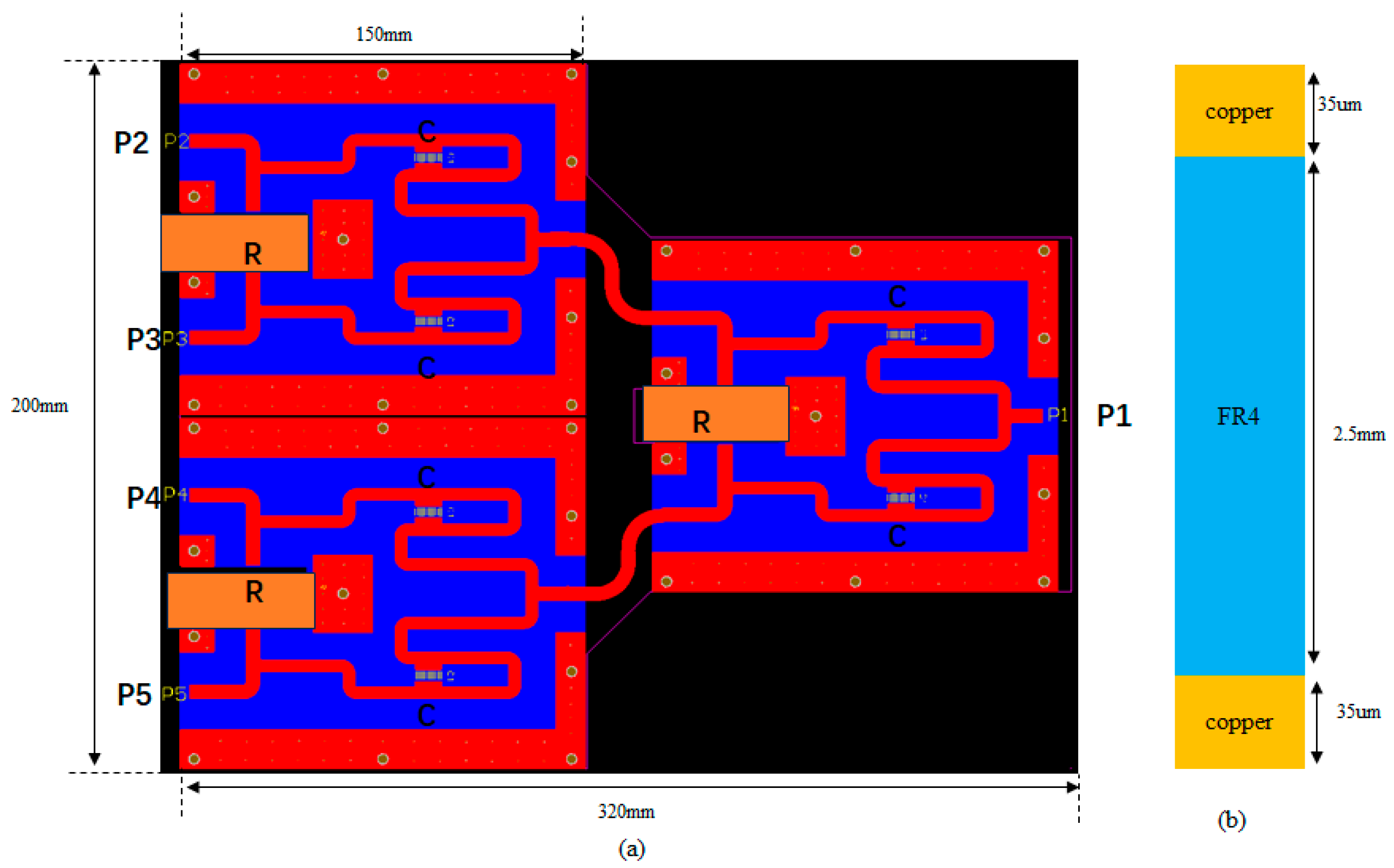
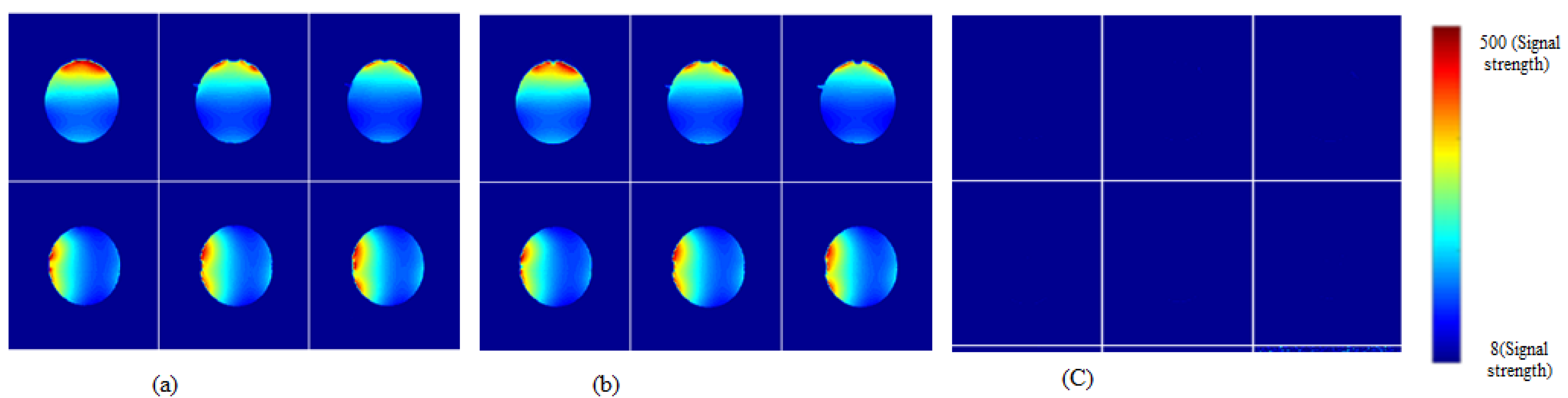
In summary, to address the challenges of bulky dimensions, high loss, and thermal management in high-power, MHz-range MRI applications, this study proposes a capacitor-loaded microstrip hybrid structure by integrating transmission line theory with lumped-element capacitor principles. The compact 3.0T RF combiner was designed by optimizing the microstrip width for a fixed substrate thickness, achieving high power density (8 kW) and low insertion loss (0.4 dB) at the operation bandwidth and minimizing its footprint (320 × 200 × 10 mm). Its high-power capability was analyzed through thermal management. The implemented combiner was successfully integrated into a 3.0T MRI RFPA system and reduced the RFPA’s total dimensions, further improving imaging validation to achieve good quality. Although this approach narrows the bandwidth, the optimized combiner remains fully compatible with MRI systems due to their inherent narrowband operation.

2. Methods

2.1. Theory Analysis of Combiner Branch

A multi-way combiner comprises multiple branches and isolation resistors according to RF combiner theory. These branches may utilize either lumped-parameter elements or transmission-line structures, or both. Consequently, the fundamental performance of an individual branch was prioritized for analysis.

2.1.1. Impedance Transformation Analysis

In a combiner, conventional 50 Ω RF networks employ 70.7 Ω quarter-wavelength lines for the 50 Ω to 100 Ω impedance transformation. This function is realized through a capacitor-loaded parallel microstrip structure, such as that shown in Figure 1, which simultaneously widens the lines and shortens their lengths.
To achieve an impedance transformation of 50 Ω to 100 Ω at the operating frequency, a multi-section microstrip structure with lumped capacitive compensation was proposed, as shown in Figure 1. The design comprised two microstrip lines (electrical length βl₁), one line (βl₂), and a shunt capacitor C, all sharing the characteristic impedance Z₀. Through the optimization of βl₁, βl₂, Z₀, and C, impedance matching between the source (Zₛ = 50 Ω) and load (Zₗ = 100 Ω) was realized. The analytical process is detailed below:
(1) After passing through the transmission line βl1, the load Zl satisfies the following [13,14]:
Z i n 2 = Z 0 Z l + Z 0 tan β l 1 Z 0 + Z l tan β l 1
(2) As one terminal of the capacitor C is connected to point B, the following relationship holds:
Z c = 1 j ω C
(3) By equivalently transforming the capacitor to point B, the total impedance at point B can be expressed as follows:
  1 Z B = 1 Z i n 2 + j ω C = > Z B = ( 1 Z B + j ω C ) 1
(4) Consequently, the input impedance of the transmission line βl2 is given by the following:
  Z i n 1 = Z 0 Z B + Z 0 tan β l 2 Z 0 + Z B tan β l 2
(5) The final expression for the source impedance Zs is as follows:
Z s = Z 0 Z i n 1 + Z 0 tan β l 1 Z 0 + Z i n 1 tan β l 1  
Substituting Equations (1)–(4) into (5) yields the complete Zs-Zl relationship. Setting the right Zs and Zl, the target impedance transformation can be achieved by optimizing βl1, βl2, Z0, and C. Of course, multiple parameter sets satisfy Equation (5), enabling selection based on criteria such as the characteristic impedance, bandwidth, power capability, and capacitance value.

2.1.2. The Bandwidth Analysis

Based on the preceding analysis, the intermediate section of the microstrip line and parallel-connected capacitor is illustrated below in Figure 2.
The microstrip line has a characteristic impedance Z0, the electrical length is βl₂, the input impedance is Zin1, and the output impedance is Zin2. By treating this two-port network as a parallel configuration, the admittance matrices of the capacitor and microstrip line are calculated separately. Using the Kuroda identity transformation [15], the total admittance matrix is synthesized as follows:
Y t o t a l = j Y 0 cos β l 2 + j ω C j Y 0 sin β l 2 j ω C j Y 0 csc β l 2 j ω C j Y 0 cot β l 2 + j ω C
where Y0 = 1/Z0,ω is the operation frequency.
The input impedance Zin1 is determined by the total admittance matrix and Zin2:
Z i n 1 = Z 0 ( Z i n 2 + j Z 0 tan β l 2 ) + 1 j ω C ( Z 0 + j Z i n 2 tan β l 2 ) Z 0 + j Z i n 2 tan β l 2 + j ω C ( Z i n 2 + j Z 0 tan β l 2 )
Under the conjugate matching condition Zin1 = Zin2, the reflection coefficient Γ is defined as follows:
Γ = Z i n 1 Z i n 2 Z i n 1 + Z i n 2
The bandwidth Δf is defined as the frequency range where ∣Γ∣ < Γmax. Assuming a small electrical length βl2 ≪ 1 wavelength, the approximate bandwidth formula is as follows:
f C 2 π β l 2 ϵ e f f · Z 0 R e Z i n 2 + Z 0 2 ω 0 C
where ε e f f is the equivalent dielectric constant, Re(Zin2) is the real part of the load impedance, and ω0 is the center angular frequency. Thus, the characteristic impedance Z0 is proportional to the bandwidth, while C and βl₂ are directly and inversely proportional to the bandwidth.

2.1.3. Insertion Loss Analysis

In the working frequency range, the microstrip line loss is the sum of the conductor loss and the dielectric loss. The conductor loss is governed by the transmission line geometry (length/width), while the dielectric loss depends on substrate properties, which can be expressed as follows [16,17]:
T o t a l l o s s = 8.686 c + d · l = 8.686 ( R s Z 0 · ω + π f ε r tan δ c ε e f f ) · l
where ε r is the relative dielectric constant; tanδ is the loss tangent (frequency-dependent); C is the speed of light; ε e f f has the same definition as Equation (9); Rs is the surface resistance, determined according to the vacuum magnetic permeability (μ0) and the conductivity of the metal (σ); and Z0 is the characteristic impedance of the microstrip line.
To achieve high-power, low-loss performance, the design of a combiner that reduces the line length, increases the line width, and utilizes a substrate material with lower tanδ is critical in Equation (10). The design detailed in the model in Figure 1 was achieved via Equations (5) and (10), assuming that the microstrip substrate material was FR4(ε = 4.4, tanδ = 0.016), its thickness was h, the copper thickness was 35 um, and the microstrip width was w. As a result, the conductor losses could be reduced by utilizing parallel capacitors, widening the line width, and shortening the line length. With Zs = 50, the parameters βl1, βl2, Z0, Zl, w, h, and C could be calculated, as summarized in Table 1. Increasing the shunt capacitance reduced the total microstrip electrical length (e.g., the total angle from 90° for λ/4 lines in Group 1 to 60–75° in Groups 2–5). Lowering Z0 (e.g., 70.7 Ω → 49 Ω) widened the line width, improving power handling. Concurrently, shorter microstrip lengths minimized conductor losses, enabling synergistic low-loss and high-power performance.

2.1.4. High-Power Capability Analysis

The high-power capability is dependent on the safe thermal accumulation, while excessive thermal accumulation is suppressed by the lower IL level, thereby enhancing power capacity. The high-power capability is primarily constrained by thermal safety considerations [18,19].
The combiner surface temperature must be controlled below Tmax. Subsequently, the combiner surface temperature must maintain compliance with Tmax limitations, whether considering Tpeak or Tavg—specifically, Tpeak ≤ Tmax and Tavg ≤ Tmax. Here, Tpeak represents the transient peak temperature, while Tavg denotes the average temperature.
The transient peak power is expressed as:
P p e a k , m a x = C t o t a l . T m a x T a m b T p u l s e
The average power is defined as:
P a v g , m a x = T m a x T a m b R θ , t o t a l
where Rθ,total is the system’s thermal resistance, which is relevant to the thermal cooling; in general, it is around 0.1 °C/W.
To address the high-power capability, the single-branch microstrip of Table 1 was analyzed. The ambient temperature was assumed to be 20 °C, with a maximum operating temperature Tmax = 50 °C. The design could withstand a large peak power Ppeak = 5 KW at a 5% duty cycle, yielding an average power of 250 W.
The FR4 material’s properties were Rθ,total = 0.1 °C/W, Cp = 1, and ρ = 1.85 g/cm3, and the heat capacity—Cvol—is described below:
C V o l = ρ . C p = 1.85 J c m 3
The volume of the substrate of FR4 was 7.56 cm3 (l × w1 × h: w1 = 20 mm, h = 2.5 mm, and L = 2l1 + l2 = 201.5 mm); thus, the heat capacity Ctotal is as follows:
C t o t a l = V . C v o l = 10.08 J ° C
The power limits were calculated using Equations (11) and (12).
The single-branch Ppeak,max was 6.05 kW per branch. With four input ports combined into two output ports, the total peak power Ppeak,max reached 12.10 kW, while the average power Pavg,max for the two output ports was approximately 300 W.
Typically, a two-way combiner comprises two branches. When operating under high-power transmission conditions with a peak power of 6.05 kW (and an average power exceeding 300 W), the signal branch design can achieve approximately 6 kW high-power transmission provided that the internal temperature rise remains within 30 °C.

2.2. Optimization Analysis at the 3.0T MRI Operation Frequency Band

Theoretical analysis confirmed that the microstrip shunt capacitor structure achieved combiner impedance transformation while expanding the line width and shortening its length, enhancing the power capacity and reducing the size. However, the multi-variable coupling in Figure 2 makes analytical solutions to Equations (1)–(5) impractical. Therefore, high-power, low-loss constrained optimization was implemented via ADS simulation:
(1)
The microstrip width range was set to W = 6~10 mm due to the high-power capability; the substrate thickness was fixed to h = 2.5 mm (PCB limitations).
(2)
The optimization framework @3.0T frequency was set to 128 ± 1 MHz; Zs = 50 Ω; Zl = 100 Ω.
(3)
S11 << −25 dB, S21 ≤ 0.05 dB, and S22 < −25 dB were set.
(4)
The Z0 range was set to 30~70.7 Ω, and the capacitance was set to the range C = 1–1000 pF.
(5)
The total microstrip length electrical angle limitation was set as follows: 2βll + βl2 < 70°.
The iterative optimization of C, βl1, βl2, and line width under the constraints finalized the high-power combiner design. ADS simulation models based on Figure 1 were established, with the results in Table 2 confirming all performance targets were met.
The microstrip was designed based on the parameters in Table 2, employing a 35 μm thick copper layer and FR4 substrate. Simulations were performed, producing results aligned with Table 3, where l1 and l2 are the length of the microstrip, h is the thickness of the substrate, w is the width of the microstrip, and C is the capacitor.
It can be observed that the microstrip line length in this design was reduced by 30% compared to the conventional quarter-wavelength line, and the IL(S21) was simultaneously decreased to 0.1 dB when using the FR4.

2.3. Design and Fabrication of the Combiner

2.3.1. The 4 to 1 Combiner Design

Based on the above analysis, the four-way to one-way combiner was composed of three two-way to one-way combiners, and the two-way to one-way combiner was designed with two branches and an isolation resistor, as shown in Figure 3.
In this design, ports P2 and P3 are inputs, and P1 is the combined output. The source and load impedances (Zs, Zl) are 50 Ω, with a 100 Ω power resistor. The remaining microstrip lines have characteristic impedance Z0 and lengths βl1, βl2, and βl3. Each Z0 line is paired with capacitor C. The combiner’s output power must exceed 69.1 dBm, while the power resistor requires ≥400 W on average and ~8000 W peak dissipation (duty cycle ≤ 5%) for MRI application.
Based on ADS simulations, Z0 was determined as 45 Ω with a corresponding line width of ~6 mm. A two-way to one-way combiner 3D model (Figure 4) was established in HFSS for optimization, and the model uses the FR4 substrate with an ideal copper conductor at the bottom. The top layer includes golden copper microstrip lines of lengths l1 and l2, a 35μm-thick conductor layer, and incorporates a 100 Ω ideal resistor (R) and a capacitor (C) in its structure. The simulation process retains conditions (1), (2), (4), and (5), while condition (3) was adjusted to a 4~10 mm line width range. Ports P1~P3 were assigned, with the combiner parameters and S-parameter results summarized in Table 4 and Table 5, respectively.
Table 5 confirms compliance with all the performance requirements. Post simulation, three two-to-one combiners were cascaded into a four-way configuration with a total loss of ~0.4 dB. The PCB design like as Figure 5, red zone is the 35 um thickness copper of top layer, and bottom layer is 35 um thickness of copper as ground. The PCB demonstrated a ~30% microstrip length reduction via capacitor C, which is a high-Q-value ceramic capacitor such as the ATC 100C, resulting in a compact two-way combiner with a size of 150 × 100 × 10 mm and the four-way input (P2~P5), with the P1 as the combiner output.

2.3.2. Fabrication and Measurement

The fabricated four-way combiner PCB (FR4 substrate and 35 um copper layer) measured 300 × 200 × 10 mm. Performance characterization was performed using an E5071 network analyzer (Keysight Technologies, Santa Rosa, CA, USA). The test bench like as Figure 6, and performance evaluation of the P5 port is achievable by interchanging the connections between P4 and P5 ports. Final, the test results summarized in Table 6.
The results in Table 6 show an insertion loss of 6.30~6.40 dB, a port VSWR of <20 dB, and isolation >–25 dB, with the loss significantly reduced compared to conventional designs.

2.3.3. High-Power Capability Validation

The high-power test bench, as depicted in Figure 7, features the orange-highlighted combiner investigated in this study. The instrumentation comprises an E4438 RF signal generator, N9020 spectrum analyzer (Keysight Technologies, Santa Rosa, CA, USA), and SHX10K10 high-power attenuator load (SHHX, Shanghai, China). and the orange part is the combiner studied in this paper. As the core of the 3.0T MRI RFPA, combined the RF input (RFin) via a driver amplifier (PAd) and 1:4 divider to four PAs (PA1–PA4), achieving large power (large than 69.2 dBm) output (RFout). To verify the power handling capacity of the combiner, temperature changes and output power variations were tested under different voltage standing wave ratio (VSWR) conditions at full power output. Under 128 MHz pulsed operation (5% duty cycle) with water cooling (inlet at 30 °C), the PA1–PA4 outputs at 63.6 dBm yielded a 69.2 dBm combiner output when the input power was 0 dBm.
Fiber-optic temperature probes were used to measure thermal profiles at three resistors and the output microstrip (four positions, Figure 8), with data collected at 0, 10, 20, 30, and 60 min. The temperature variations across the four test points are shown in Figure 9, while power variations (from 0 to 60 min) are summarized in Table 7, and at VSWR = 1:1.2, Pmax measured 69.2 dBm, and Pmin measured 69.11 dBm (ΔP = 0.09 dB). At VSWR = 1:2, Pmax measured 68.69 dBm, and Pmin measured 68.60 dBm (ΔP = 0.09 dB), demonstrating minimal power variation.
It can be observed that, for VSWR values of 1:1.2 and 1:2, the temperature rise at the test points remained below 1 °C over 60 min, and the power fluctuation did not exceed 0.1 dB from Table 7. These results demonstrate that the developed high-power combiner exhibits excellent thermal stability and power integrity under demanding operational conditions.

2.4. Study of RFPA with Combiner MRI Experiments

2.4.1. High Power and Linearity Analysis of RFPA

The high-power, small-size MRI combiner studied in this work adopted a planar circuit and capacitor loading structure. This design enabled integration with the RF amplifier section of the MRI RFPA on the same PCB, as illustrated in Figure 7, contributing to the miniaturization of the entire MRI RFPA device. By reducing losses in the key combiner of the high-power output section, the overall efficiency of the MRI RFPA could be enhanced. Simultaneously, the resultant heat reduction from decreased losses improved the RFPA’s nonlinearity characteristics.
To validate the linearity characteristics of high-power combiners in RFPA systems, a magnetic-core combiner from Xingaoyi medical equipment company (Ningbo City, China) was implemented. This device demonstrated an insertion loss of 0.6 dB at 128 MHz, and comparative testing under identical conditions revealed nonlinear behavior. When the RFPA input power reached 0 dBm (achieving maximum output), the combiners’ power responses were measured at 10, 20, 30, and 60 min operational intervals as shown in Table 8.
As demonstrated in Table 8, the proposed combiner achieved approximately 0.2 dB higher output power than the magnetic-core counterpart, attributed to its lower insertion loss. Regarding linearity performance, the proposed design maintained output variations below 0.05 dB during extended operation, whereas the magnetic-core structure showed a 0.18 dB drift. This confirms that ferrite components develop nonlinear characteristics under thermal variations.

2.4.2. MRI Experiments for RFPA

This device was directly embedded into the MRI system for imaging experiments, significantly enhancing the overall system efficiency. The assembled RFPA was incorporated into the 3.0T MRI platform (Figure 10). To validate its performance, imaging experiments were conducted using the gradient recalled echo (GRE) sequence, with the results displayed in Figure 11. These images were compared against those from the existing RFPA device. As shown in Figure 11, both systems exhibited comparable image quality. Further comparisons of the excitation efficiency and signal-to-noise ratio (SNR) are detailed in Table 9.
The results in Table 9 indicate similar SNR values between the two devices; however, the RFPA with the proposed combiner demonstrates superior excitation efficiency due to its lower insertion loss (IL).

3. Performance Analysis

This work presents a high-power combiner for 3.0T MRI systems, and a comparison of its performance with respect to conventional designs is presented in Table 10. The proposed combiner achieves superior compactness, efficiency, and integration, enabling system-level high-power output. Integrated into RFPA systems, it enhances power-combining efficiency while reducing system volume.
Table 10 highlights the proposed high-power combiner’s advantages in compactness, performance, and system integration. The combiner enables final-stage power combining to meet high-power requirements and, when integrated into RFPA systems, enhances the combining efficiency while reducing equipment size. To quantify these benefits, a figure of merit (FoM) was established as a weighted product of critical metrics:
F o M = 1 I n s e r t i o n   L o s s     C o m b i n i n g   E f f i c i e n c y     I n t e g r a t i o n   F a c t o r   1 N o r m a l i z e d   V o l u m e
where
  • insertion loss (IL): lower is better → inversely proportional term (1/IL);
  • combining efficiency (η): direct percentage value (e.g., 91% → 0.91);
  • integration factor (IF): IF = 1.2 for fully integrated designs (e.g., our work, [18]);
  • IF = 1.0 for non-integrated designs (e.g., [19,20]);
Normalized volume (V):
The volume was calculated as L × W × H and then normalized to the largest volume in the table (e.g., [19,20]: 200 × 200 × 40 = 1.6 × 106 mm3):
V n o r m = V o l u m e   o f   D e s i g n M a x   V o l u m e  
This FoM emphasizes low insertion loss, high efficiency, full integration, and compactness. Table 11 shows that the proposed design achieved an FoM of 6.83, surpassing the next best design ([19], FoM = 4.0) by 1.5× and non-integrated counterparts ([20,21,22], FoM = 1.45) by 4×. These results highlight its superiority in balancing performance, integration, and miniaturization for high-power MRI systems.

4. Conclusions

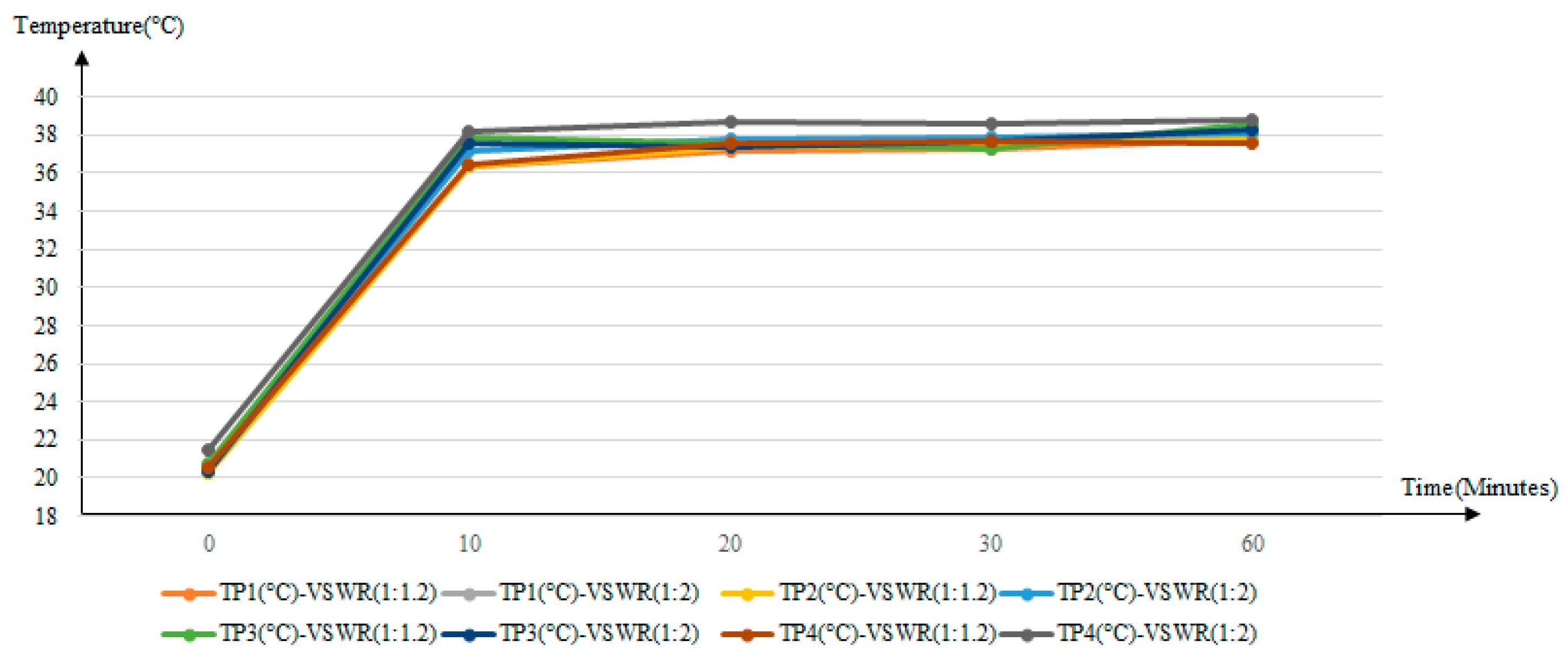
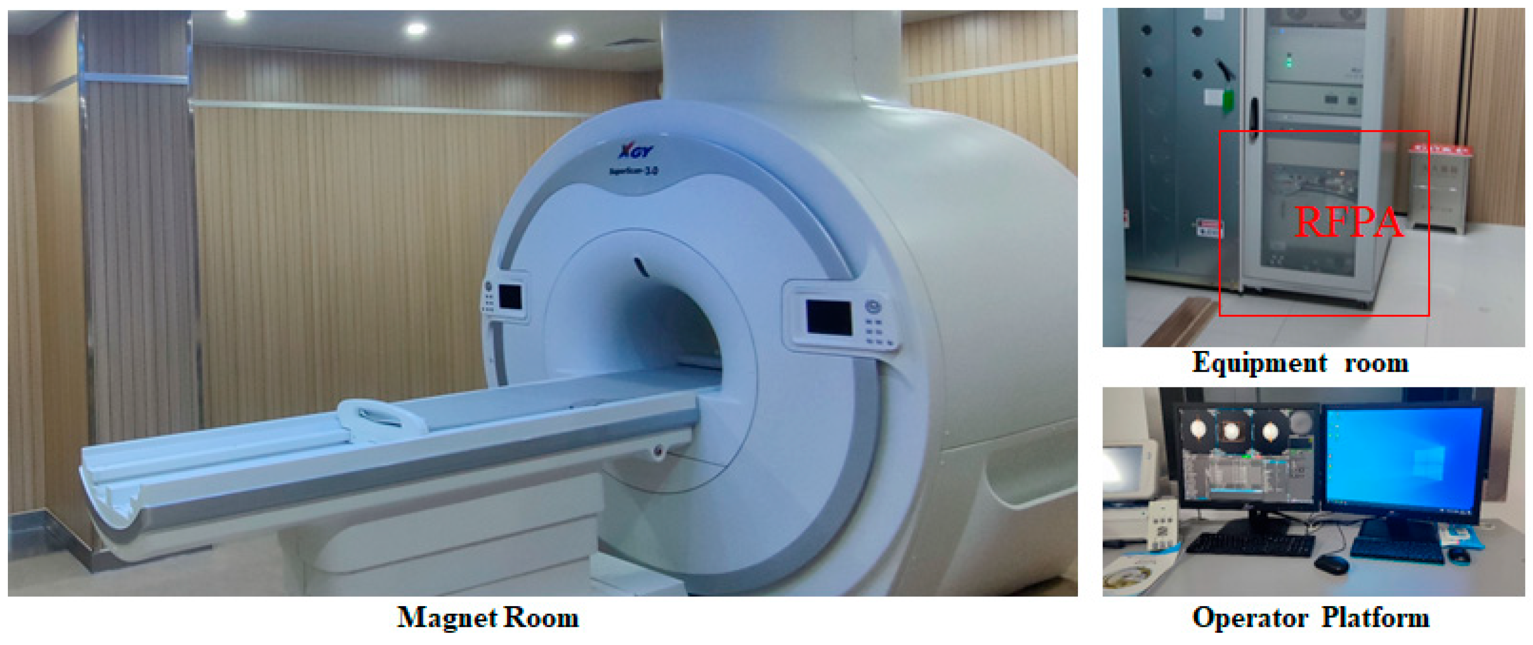
This study addresses the challenges of high loss and bulkiness in MRI RFPA combiners. Leveraging the Wilkinson combiner theory, a novel four-way microstrip capacitor-loaded combiner was designed and fabricated. Through optimization of the microstrip’s length and capacitor loading, followed by testing, the combiner achieved an insertion loss reduction of 0.4 dB (30% lower than that of conventional 0.6 dB designs), a power-handling 8 kW peak power, a compact size of 320 × 200 × 10 mm (30% smaller than its traditional counterparts), a port performance VSWR < 1.25 (equivalent to a −25 dB return loss), and isolation >30 dB. Finally, the RF combiner was integrated into the RFPA system to achieve the bulk volume, and then imaging experiments were conducted with the 3.0T MRI system; this RFPA combiner demonstrated high efficiency due to lower loss.
The capacitor-loading technique optimizes the microstrip’s electrical parameters, balancing loss and size for high-field MRI systems. Future research directions include scaling to multi-stage combiners for higher-channel MRI systems, adjusting the capacitor-loaded microstrip length Z0 and structures to make them adaptable to 1.5T~7.0T MRI systems, and microchannel cooling or Low Temperature Co-fire Ceramic (LTCC) processes for 8 kW plus thermal stability. This design methodology can extend to RF ablation and communication systems, advancing high-power RF devices toward miniaturization and low-loss operation.

Author Contributions

Writing—review & editing, Y.L.; Supervision, S.L. All authors have read and agreed to the published version of the manuscript.

Funding

This work was supported by the MRI 3.0T Super Scan Project of Xingaoyi Medical Equipment Co., Ltd., China (No. XGY3T2018001), the Key Project of the Ministry of Science and Technology of China, “Liquid Helium-free Magnets and Their Integrated Systems” (No. 2019YFC0118700), Ningbo Key Research and Development Program (Unveiling and Leading)-Development of a 3T Vertical Brain-Dedicated Innovative Liquid Helium-Free Nuclear Magnetic Resonance Imaging System (No. 2023Z182) and National Key Research and Development Program for Technology-based SMEs-Development of a Liquid Helium-Free Superconducting 3.0T Brain Structure and Function-Dedicated Magnet (No. 2022YFC2408900). The design was simulated using ANSYS HFSS 2019 R1 for 3D electromagnetic analysis and co-optimized with Keysight ADS 2018; the critical parameters were validated.

Institutional Review Board Statement

Not applicable.

Informed Consent Statement

Not applicable.

Data Availability Statement

The original contributions presented in this study are included in the article. Further inquiries can be directed to the corresponding author.

Conflicts of Interest

The authors declare no conflict of interest.

References

  1. Boricha, V.D.; Jadhav, R.A.; Vishwakarma, R.; Bhuiya, T.K.; Harsh, R. Power Dividers/Combiners for 1. In 5T MRI Solid State Power Amplifier. In Proceedings of the 2018 2nd International Conference on Electronics, Materials Engineering & Nano-Technology (IEMENTech), Kolkata, India, 4–5 May 2018; pp. 1–5. [Google Scholar]
  2. Li, Y.; Luo, S.; Liu, C.; Ye, Y. Design and Realization of Time-domain Transfer DPD Method for MRI RF Power Amplifiers. In Proceedings of the 2023 6th International Conference on Electronics Technology (ICET), Chengdu, China, 12–15 May 2023; pp. 490–494. [Google Scholar]
  3. Wang, T.H.; Chen, J.H. Power recycling using Wilkinson power combiner with pulse width modulation. In Proceedings of the 2017 IEEE International Symposium on Radio-Frequency Integration Technology (RFIT), Seoul, Republic of Korea, 30 August–1 September 2017; pp. 223–225. [Google Scholar]
  4. Wang, L.C.; Zhu, G.J.; Wang, J.; Li, B. Evaluation and simulation of eight-element phased-array surface coil in 3. 0T MRI. In Proceedings of 2012 IEEE-EMBS International Conference on Biomedical and Health Informatics, Hong Kong, China, 5–7 January 2012; pp. 659–662. [Google Scholar]
  5. Zhang, Y.; Zhang, Z.; Yuan, Z.; Wang, X.; Li, S. Modeling and Design of High-Power Non-Isolating RF Power Combiners based on Transmission Lines. In Proceedings of the 2022 IEEE Applied Power Electronics Conference and Exposition (APEC), Houston, TX, USA, 20–24 March 2022; pp. 259–266. [Google Scholar]
  6. Twieg, M.; Griswold, M.A. High efficiency radiofrequency power amplifier module for parallel transmit arrays at 3 Tesla. Magn. Reason. Med. 2017, 78, 1589–1598. [Google Scholar] [CrossRef] [PubMed]
  7. Carpenter, T.; Williams, E. MRI–From basic knowledge to advanced strategies: Hardware. Eur. Radiol. 1999, 9, 1015–1019. [Google Scholar] [CrossRef] [PubMed]
  8. Vani, R.; Meenakshi, S.; Shree Sahitya, B. 4-Way Ka-Band Power Combiner Using Rectangular Waveguide. In Proceedings of the 2024 4th International Conference on Intelligent Technologies (CONIT), Bangalore, India, 21–22 June 2024; pp. 1–4. [Google Scholar]
  9. Wang, F.; Zhang, X.; Wang, X. A Novel Multi-Section Lumped Element Topology for Wilkinson Power Divider Design. In Proceedings of the 2023 16th UK-Europe-China Workshop on Millimeter Waves and Terahertz Technologies (UCMMT), Guangzhou, China, 13–15 September 2023; pp. 1–6. [Google Scholar]
  10. Joshi, P.; Mathew, J.V.; Kumar, R. Design and development of high bandwidth coaxial RF combiner. J. Instrum. 2025, 20, 03013. [Google Scholar] [CrossRef]
  11. Zhang, H.; Cassidy, G.; Jurkov, A. A High-Power Nonisolating RF Power Combining Network Based on Transmission Lines. IEEE J. Emerg. Sel. Top. Ind. Electron. 2023, 5, 1006–1016. [Google Scholar] [CrossRef]
  12. Choi, C.-H.; Webb, A.; Orzada, S.; Kelenjeridze, M.; Shah, N.J.; Felder, J. A Review of Parallel Transmit Arrays for Ultra-High Field MR Imaging. IEEE Rev. Biomed. Eng. 2024, 17, 351–368. [Google Scholar] [CrossRef] [PubMed]
  13. Damm, C.; Freese, J.; Schussler, M.; Jakoby, R. Electrically Controllable Artificial Transmission Line Transformer for Matching Purposes. IEEE Trans. Microw. Theory Tech. 2007, 55, 1348–1354. [Google Scholar] [CrossRef]
  14. Tang, Y.; Xia, B.; You, M. Impedance model of complex grid network based on transfer matrix. In Proceedings of the 2024 6th International Conference on Energy, Power and Grid (ICEPG), Guangzhou, China, 18–22 July 2024; pp. 1654–1657. [Google Scholar]
  15. Milosavljevic, Z.D.; Gmitrovic, M.V. Design of microwave diplexers based on new Kuroda’s identities. In Proceedings of the MELECON ’98. 9th Mediterranean Electrotechnical Conference. Proceedings (Cat. No.98CH36056), Tel-Aviv, Israel, 12–15 May 1998; pp. 513–517. [Google Scholar]
  16. Rautio, J.C.; Demir, V. Microstrip conductor loss models for electromagnetic analysis. IEEE Trans. Microw. Theory Technol. 2003, 51, 915–921. [Google Scholar] [CrossRef]
  17. Kobayashi, M. A dispersion formula satisfying recent requirements in microstrip CAD. IEEE Trans. Microw. Theory Technol. 1988, 8, 1246–1250. [Google Scholar] [CrossRef]
  18. Gerstenmaier, Y.C.; Castellazzi, A.; Wachutka, G.K.M. Electrothermal simulation of multichip-modules with novel transient thermal model and time-dependent boundary conditions. IEEE Trans. Power Electron. 2006, 21, 45–55. [Google Scholar] [CrossRef]
  19. Prejs, A.; Wood, S.; Pengelly, R.; Pribble, W. Thermal analysis and its application to high power GaN HEMT amplifiers. In Proceedings of the 2009 IEEE MTT-S International Microwave Symposium Digest, Boston, MA, USA, 7–12 June 2009; pp. 917–920. [Google Scholar] [CrossRef]
  20. Li, L.Y. Research on Planar Microwave Power Combining Technology; Southwest University of Science and Technology: Mianyang, China, 2021. [Google Scholar]
  21. Xiao, W. Design and Research of High-Power Microstrip Power Dividers; Anhui University: Hefei, China, 2019. [Google Scholar]
  22. Surakitbovorn, K.; Juan, M.; Rivas, D. A Simple Method to Combine the Output Power from Multiple Class-E Power Amplifiers. IEEE J. Emerg. Sel. Top. Power Electron. 2022, 10, 2245–2252. [Google Scholar]
Figure 1. High-power microstrip line hybrid structure with lumped capacitive loading.
Applsci 15 05940 g001
Figure 2. Bandwidth analysis of structure.
Applsci 15 05940 g002
Figure 3. Hybrid capacitive-loaded microstrip combiner.
Applsci 15 05940 g003
Figure 4. Two-to-one combiner HFSS simulation model.
Applsci 15 05940 g004
Figure 5. The PCB of Hierarchical four-way combiner. (a) Top view; (b) Cross-section.
Applsci 15 05940 g005
Figure 6. Four-way combiner and testing bench.
Applsci 15 05940 g006
Figure 7. Application of the combiner in MRI RFPA and test bench.
Applsci 15 05940 g007
Figure 8. Temperature test point for high-power output.
Applsci 15 05940 g008
Figure 9. Temperature tests in different locations and with different VSWRs.
Applsci 15 05940 g009
Figure 10. 3.0T integrated imaging experimental platform.
Applsci 15 05940 g010
Figure 11. GRE sequence imaging. (a) Imaging results for the RFPA device integrated with the combiner proposed in this study; (b) imaging results for the original RFPA; (c) pixel-wise difference between (a,b).
Applsci 15 05940 g011
Table 1. Branch model results.
Group.Zs (Ω)2βl1 (°)βl2 (°)C (pF)Z0 (Ω)Zl (Ω)Angle (°)h (mm)w (mm)IL (dB)
1506030070.7100902.52.500.10
25050253551101 + j*4.3752.54.550.083
3504020355171 − j*10602.54.550.071
45040204851105.3 − j*15.8602.54.550.071
5504020484986.7 − j*12602.54.900.069
Table 2. Simulation results for a single ideal microstrip branch of the combiner.
ParameterZ0 (Ω)βl1 (°)βl2 (°)C (pF)S11/S22 (dB)S21 (dB)
Data43192064<−28<0.08
Table 3. Simulation results for a single FR4 microstrip branch of the combiner.
ParameterZ0 (Ω)l1 (mm)l2 (mm)h (mm)W (mm)C (pF)S11/S22 (dB)S21 (dB)
Data436669.52.56.067<−28<0.08
Table 4. Design parameters of the two-to-one combiner.
Combiner Parameterl2 Width/Length (mm)l1 Width/Length (mm)C (pF)MaterialThickness (mm)R (Ω)
Data6.2/666.2/69.567FR42.5100
Table 5. Two-to-one combiner simulation results@128 MHz ± 1 MHz.
S ParameterS11/S22/S33/S44 (dB)S21/S31/S41/S51 (dB)S23/S24/S25 (dB)S34/S35 (dB)
Results<−25>−6.2<−25<−25
Table 6. Four-way combiner test results @127~129 MHz.
IndexS11/S22/S33/S44 (dB)S21/S31/S41/S51 (dB)S23/S24/S25 (dB)S34/S35 (dB)
Simulation results<−256.30~6.32<-25<−25
Test results−26.56.38~6.40−27−28.3
Table 7. Power variation test results @128 MHz, with a 5% duty cycle.
Time (Minutes)RF In(dBm)RF Out (dBm)-VSWR (1:1.2)RF Out (dBm)-VSWR (1:2)
0069.268.69
10069.1568.64
20069.1768.66
30069.1468.63
60069.1168.60
Table 8. The 3.0T RFPA test results @128 MHz, with a 5% duty cycle and maxim ≈ 69.2 dBm.
RFPA withinitinal10 min20 min30 min60 minΔ (max–min)
With ferrite core69.02 (dBm)68.91 (dBm)68.93 (dBm)68.87 (dBm)68.84 (dBm)0.18 (dB)
With this work69.2 (dBm)69.21 (dBm)69.18 (dBm)69.18 (dBm)69.17 (dBm)0.04 (dB)
Table 9. Comparison of excitation efficiency and SNR.
Power Amplifier ModelDimensions (L × W × D: mm)Receive CoilPhantom ModelSNRExcitation Efficiency
Original RFPA480 × 480 × 70016-channel Head Coil00139092%
RFPA with combiner450 × 480 × 60016-channel Head Coil00139698%
Table 10. Performance comparison of this work.
Combiner TypeInsertion Loss (dB)Port VSWR (dB)Dimensions (mm) (L × W × H)Integration with RFPAIsolationIntegrated RFPA Output Power Capability (kW)Combining EfficiencyRFPA Module Size (mm)
Microstrip Combiner (4 to 1) [18]≥0.6 dB<−25 dB350 × 200 × 10Fully Integrated>25 dBHigh (>8 kW)87%350 × 250 × 25
Lumped-Element Combiner (4 to 1) [19,20]≥0.6 dB<−25 dB200 × 200 × 40Not Integrated>25 dBHigh (>8 kW)87%350 × 250 × 45
This Work (4 to 1)≤0.4 dB<−25 dB320 × 200 × 10Fully Integrated>25 dBHigh (>8 kW)>91%320 × 200 × 25
ResultSuperiorComparableSuperiorSuperiorComparableComparableSuperiorSuperior
Table 11. FoM analysis of this work.
Combiner TypeInsertion Loss (dB)Combining EfficiencyIntegration FactorNormalized VolumeFoM
Microstrip Combiner [18]0.687% (0.87)1.20.444.0
Lumped-Element [19,20,21]0.687% (0.87)111.45
Magnetic Core Transformer [22]0.687% (0.87)111.45
This Work0.4>91% (0.91)1.20.46.83
Disclaimer/Publisher’s Note: The statements, opinions and data contained in all publications are solely those of the individual author(s) and contributor(s) and not of MDPI and/or the editor(s). MDPI and/or the editor(s) disclaim responsibility for any injury to people or property resulting from any ideas, methods, instructions or products referred to in the content.

