Article

High-Efficiency Quantum Dot Lasers as Comb Sources for DWDM Applications

1
Department of Electrical and Computer Engineering, University of California, Santa Barbara, CA 93106, USA
2
Intel Corporation, 2200 Mission College Blvd., Santa Clara, CA 95054, USA
*
Authors to whom correspondence should be addressed.
Appl. Sci. 2022, 12(4), 1836; https://doi.org/10.3390/app12041836
Submission received: 5 January 2022 / Revised: 25 January 2022 / Accepted: 26 January 2022 / Published: 10 February 2022
(This article belongs to the Special Issue Quantum Dot Lasers and Laser Dynamics)

Abstract

:
The trend of data center transceivers is to increase bandwidth while simultaneously decreasing their size, power consumption, and cost. While data center links have previously relied on vertical-cavity surface-emitting lasers (VCSELs) or in-plane lasers using coarse wavelength division multiplexing (WDM) to encode data, recently, dense WDM (DWDM) has moved to the forefront for next-generation links. Several approaches exist as light sources for DWDM links; DFB arrays, nonlinear microcombs, and semiconductor mode-locked lasers (MLLs). This paper focuses on quantum dot MLLs (QDMLLs), which currently offer the best efficiency, simplicity, and size. The efficiency of optical combs generated by QDMLLs is analyzed in depth in this study.

1. Introduction

Cloud-based computing continues to fuel the demand for more internet protocol traffic, thrusting hyperscale data centers into the “Zeta-byte era” [1]. To reduce power spent on input–output (IO) and to eliminate the IO bottleneck at the front panel of server rack units [2], data center links will see photonics move into electronics packages in the near future [3,4]. This seriously constrains the power consumption, footprint, and spectral efficiency of next-generation links. Significant breakthroughs in silicon photonics have led to compact, power-efficient transceivers, which benefit from the high-volume production capability of silicon [5].
One technology in particular, micro-ring modulators (MRM), has allowed silicon photonic transceivers to produce optical links with extremely high IO bandwidth per mm 2 [6]. MRMs benefit from a compact footprint and are resonant structures, allowing them to modulate a single wavelength in a dense wavelength division multiplexing (DWDM) signal, thus eliminating optical multiplexers and demultiplexers (MUX/DEMUX) [7]. This capability has dramatically increased the need for a monolithic light source that can deliver all DWDM channels. The three approaches typically considered to meet this need are distributed feedback laser (DFB) arrays, nonlinear optical frequency combs (NOFC), and semiconductor mode-locked lasers(MLLs) [8].

1.1. DFB Arrays

The archetype wavelength division multiplexing (WDM) light source, DFB arrays, are implemented in long haul, metro, and data center applications [9]. DFBs are commercially available across the entire telecom range, with wavelengths available anywhere between 760 and 14,000 nm [10]. The WDM source is formed by combining the optical outputs of many individual lasers. DFB arrays have two aspects that NOFCs and MLLs do not; namely, the ability to scale the power in each channel independently to the desired level, and showing no reduction in efficiency as the number of channels increases. They do, however, have the largest footprint, and require an MUX to combine individual channels into one fiber. Additionally, the large temperature variation inside data center racks requires control electronics to keep each individual laser aligned to the DWDM grid/MUX, increasing their energy cost per bit [11].

1.2. Nonlinear Optical Frequency Combs

As an alternative to DFB arrays, NOFC offer the ability to generate a spectrum of discrete optical frequencies separated by a fixed channel spacing. NOFCs typically employ micro-disk or micro-ring resonators, but a straight waveguide can be used in combination with an MLL [8]. They can offer extremely large bandwidth [12], the channel spacing can be adjusted over an extremely large range [13,14], and individual comb lines can offer superior optical linewidths, making them suitable for coherent communication [15]. Anomalous group velocity dispersion (GVD) Kerr solitons suffer from an inherently low efficiency [16]. Recently, normal GVD dark soliton combs have reached 41% on-chip pump-to-comb efficiency [17]. Their biggest drawback is that the power of individual lines is typically low [18], with an average power per line of about −10 dBm. The comb generated usually shows large power variation across the comb (10–20 dB); however, recent improvements have increased the power per line [17]. They also suffer from an inherently low efficiency when considering net wall plug efficiency (WPE) of the entire source. Often neglected from the calculation, the wall plug efficiency of the pump laser itself must be considered. Additionally, optical coupling losses between the laser and the NOFC further decrease the efficiency; however, integration will alleviate this [19]. Excluding pump generation and coupling, conversion efficiencies can be as high as 40–60% [17,20].

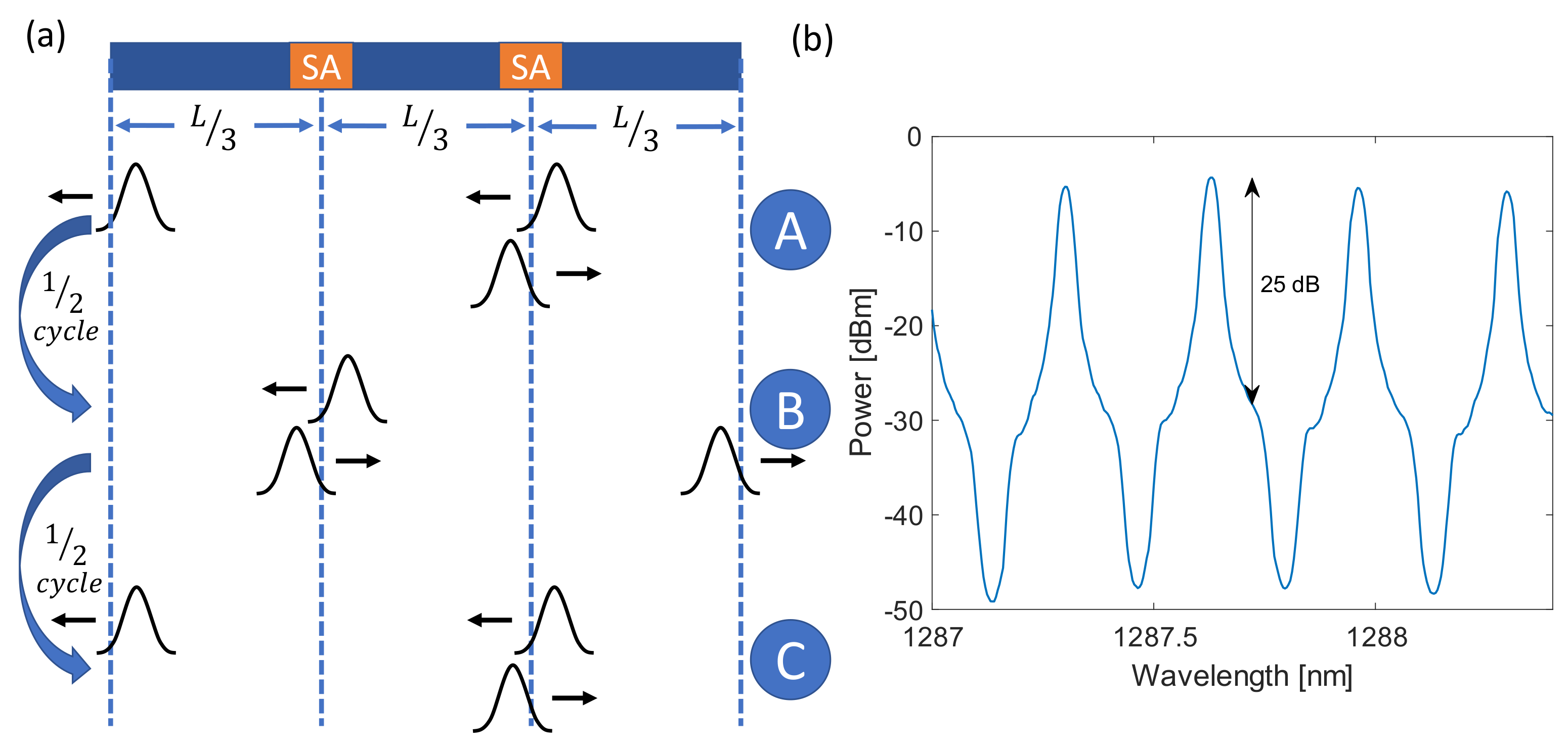
1.3. Semiconductor MLLs

Semiconductor MLLs output a high frequency pulse train with fixed frequency-spacing between the longitudinal cavity modes in a compact, efficient, reliable, and robust device, making them a natural candidate for optical sampling [21], clock distribution [22], and as DWDM sources [23]. Quantum well MLLs have been investigated for more than three decades; however, the introduction of InAs quantum dot (QD) active region has improved their performance. QDs have been shown to have higher gain [24], a lower threshold [25], a smaller linewidth enhancement factor [26], they benefit from inhomogeneous broadening [27], improved temperature-induced threshold increase (T 0 ) [28], and improved carrier dynamics [29]. Implementing InAs QDs has led to the development of efficient high-output-power MLLs, which are suitable for comb sources [8]. They output dozens of comb lines, resulting in multi-terabit single device data transmission capacities [23]. Additionally, these devices do not require initiation routines or feedback loops, and they only use voltage and current sources.

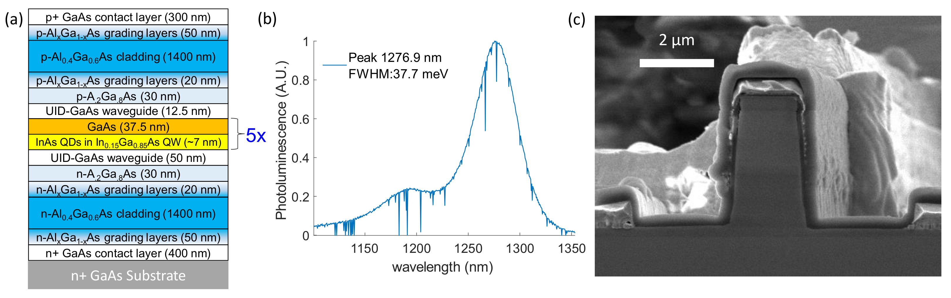
2. Device Design and Fabrication

Currently, DWDM networks typically operate at 50 or 100 GHz channel spacing and the lasers presented in this paper were designed for 60 GHz operation. When channel spacing exceeds 30–40 GHz, the cavity length becomes prohibitively short and the laser cannot emit sufficient light output from passive mode locking. In order to achieve 60 GHz spacing, colliding pulse mode locking (CPM) was employed to raise the channel spacing of lasers to multiples of the cavity FSR [30]. As an alternative to CPM, single section mode locking can also be used to achieve higher channel spacing [31]. Figure 1a shows the principle behind a colliding pulse mode-locked laser (CPMLL). The number of pulses circulating determines the harmonic (i.e., 3rd, 4th, or 5th), which is 3rd in Figure 1a. The pulses collide at interval distances of the cavity length divided by the harmonic from the output facets and saturable absorbers (SAs) are placed at these locations. For stability, the SAs closest to the two output facets must be included. The SAs at other positions in the 4th and 5th harmonic lasers can be excluded. The goal of CPM is the increase of the channel spacing of MLLs. However, the fundamental modes, which are spaced by a single FSR, are still present. These modes are considerably suppressed, as can be seen in Figure 1b. A side mode suppression ratio (SMSR) of 25 dB or greater can be achieved for optimal states.
All devices discussed were grown on nominal (001) n-doped GaAs wafers with a VEECO GenIII solid source Molecular Beam Epitaxy machine. The details of the epi-stack are shown in Figure 2a. The stack begins with a 400 nm thick, highly doped n-contact layer. The aluminum content is then graded to 40% to form the waveguide lower cladding, which is 1.4 μ m thick. The Al content is then graded to 20% for a 20 nm thick confinement layer, before the active region. The active region is 285 nm thick and contains 5 layers of (quantum) dots in a well (DWELL). The DWELL layer consists of 2.5 monolayers of InAs in a 7 nm thick In . 15 Ga . 85 As well and are separated by 37.5 nm of GaAs. The p-type cladding consists of the same Al concentrations and thicknesses, with a 300 nm thick p-type, highly doped contact layer on top. The photoluminescence of the QDs is shown in Figure 2b, and has a full width at half maximum of 38 meV.
The epi-stack was processed into deeply etched ridge lasers, as seen in Figure 2c. The ridge waveguides were formed by inductively coupled plasma etching using N 2 and Cl 2 . The etching conditions were optimized to give vertical sidewalls and reduced sidewall roughness to minimize internal loss [32]. An additional dry etch was preformed to electrically isolate the p-contact of the SA and gain section. This was accomplished by etching a 10 μ m long section of the ridge through the 300 nm p-contact layer and through 300 nm of the p-cladding. The sidewalls were first passivated with 12 nm of atomic layer deposition alumina to reduce sidewall recombination, followed by 1 μ m of sputtered SiO 2 . The contacts to the p-type and n-type layers were made by Pd/Ti/Pd/Au and Pd/Ge/Pd/Au layers to form ohmic contacts with contact resistances of about 2 × 10 5 Ω · cm 2 . The substrate was thinned to 200 μ m before cleaving to form output facets. All sample facets were left as-cleaved.

3. Performance of CPMLLs

3.1. LIV Performance
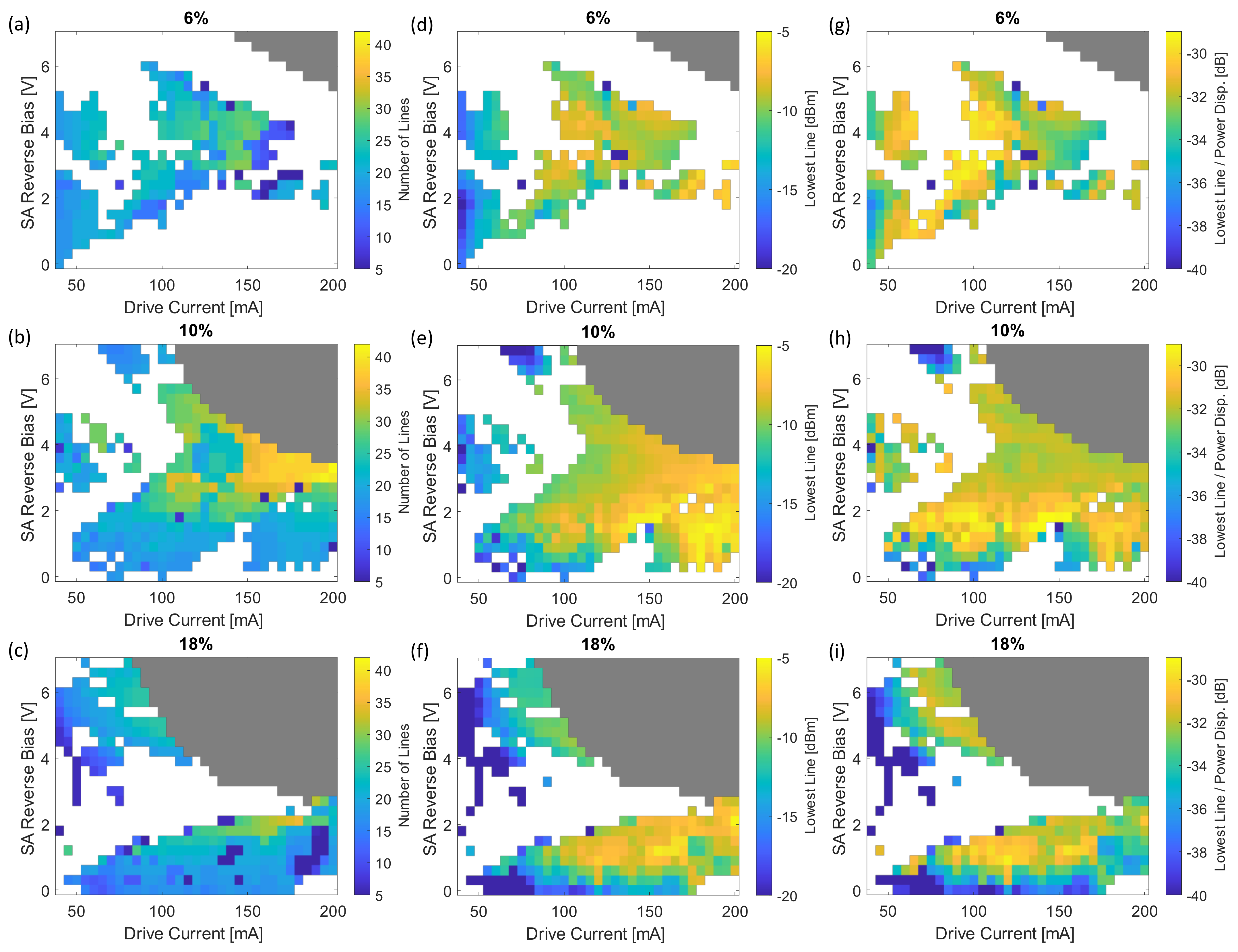
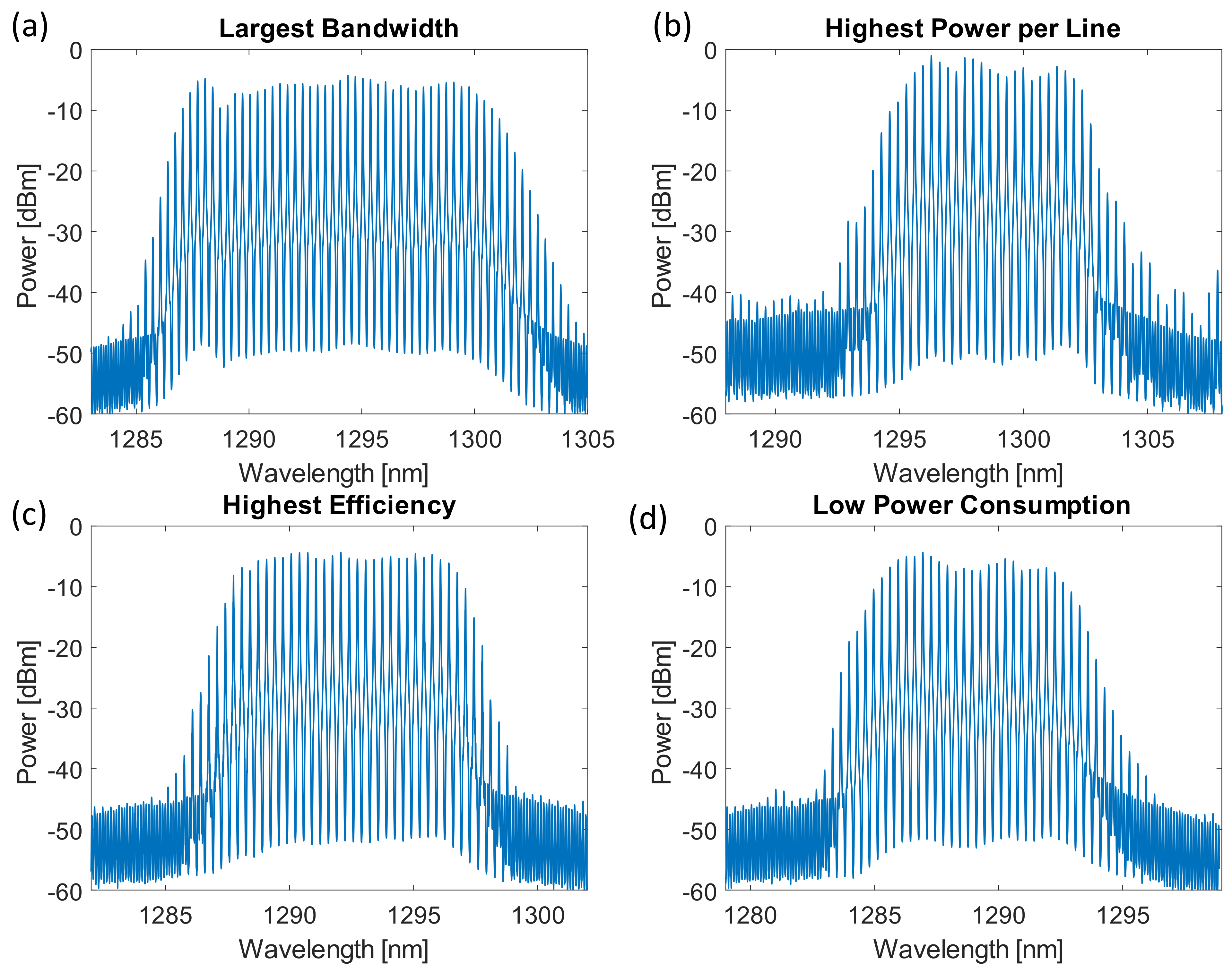
Devices were tested continuous-wave on a temperature-controlled copper heatsink at 20 °C. An integration sphere was used to measure light output, and voltage was measured in a four-wire configuration. The light–current and single-sided WPE curves for the 60 GHz 3rd harmonic CPMLLs are shown in Figure 3a,b. The total SA length, as a fraction of the cavity length (2048 μ m), is labeled on the respective curves. The performance of the devices are shown under two conditions; the first is with the SA sections connected in parallel with the gain section (labeled forward-biased), and the second is with the SA sections reverse-biased at 2 V (labeled 2 V). The forward-biased performance mimics the expected performance of Fabry–Perot lasers of the same design (i.e., lasers with no SA section). There was no significant difference in the light output or voltage between the three devices. When the SA was reverse-biased, the decrease in output power due to the SA was clear. The small penalty in efficiency imposed by the SA created equal frequency spacing between comb lines. The decrease in output power as a percentage of forward-biased power is shown in Figure 3c. When considering devices with shorter SA sections, which will later be shown to be optimal for comb generation, the decrease in output power and WPE is only in the 10–20% range.

3.2. Comb Bandwidth

In order to investigate the performance of the CPMLLs as optical frequency comb sources, optical spectra from the devices in Figure 3 were collected for varying SA reverse biases and gain section drive currents. To prevent laser damage, the states in the gray region in the upper right hand corner of Figure 4a–i were not tested. These states exceeded the maximum allowed SA current, which was conservatively set at 16 mA total. The spectra collected were filtered by removing states with less than 15 dB SMSR. For all remaining states, the number of 60 GHz channels in a 6 dB bandwidth were tabulated, and the results are shown in Figure 4a–c. The maximum and average bandwidths of the three devices are listed in Table 1. The 10% device shows the largest bandwidth, the highest average bandwidth, and the largest number of states with SMSR exceeding 15 dB. Figure 5a shows the comb with the largest achievable bandwidth of 42 comb lines, or 14.1 nm, from the 10% device at a gain current of 200 mA and an SA reverse bias of 3.3 V.

3.3. Power per Line

Of equal importance was the analysis of the power of individual comb lines of CPMLLs. Uneven power distribution between comb lines is often a limiting factor of OFCs. The optical SNR of an encoded DWM channel is, in general, proportional to the optical power. In extreme cases, comb lines with the lowest power will not be encoded with data, reducing the bandwidth and spectral efficiency of the link. To address this concern, each measured spectrum is analyzed to identify the 20 contiguous comb lines with the highest power. The power of the lowest line (PoLL) is found for each spectrum and the PoLL vs. SA bias and drive current is plotted in Figure 4d–f. The maximum recorded PoLL and the number of states with PoLL ≥ −8 dBm are recorded in Table 1. For lower bias values (50–120 mA), similar PoLL values are recorded for the 6% and 10% devices. Similarly, for higher biases, the 10% and 18% devices show similar PoLL values. The 10% device shows the highest PoLL value of −5.1 dBm and the most states (117) with PoLL ≥ −8 dBm. The PoLL values reported in Figure 4 and Table 1 are single-sided fiber-coupled power values. Devices have as-cleaved facets, with equal amounts of power emitted from both sides. This, in combination with the 2 dB fiber coupling loss, corresponds to a roughly 5 dB decrease in the reported values from the total power emitted from the device. This shows that with a high reflection coating and improved fiber coupling and device design, combs with PoLL ≥ 0 dBm are achievable. The spectrum with the highest PoLL is shown in Figure 5b from the 10% device at a 185 mA drive current and with a 1.5 V SA bias.

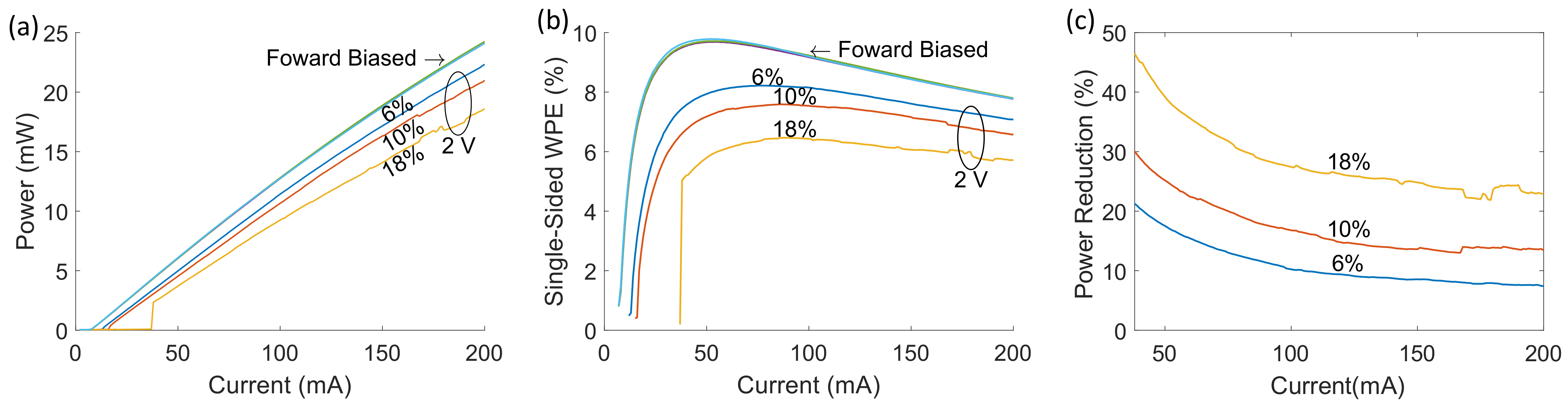
3.4. Comb Efficiency

In order to analyze the efficiency of the different devices, the WPE of comb lines was analyzed. For a given comb, the comb line with the lowest power will also have the lowest WPE. Therefore, the PoLL values in Section 3.3 are divided by the electrical power consumption of the CPMLL for each state to calculate the WPE of the 20th channel (WPE20). The WPE20 for the devices from Figure 3 are shown in Figure 4d–f, and the maximum and average WPE20 values are recorded in Table 1. All WPE20 values are stated in dB and the PoLL used to calculate WPE20 includes a 2 dB chip-to-fiber coupling loss. The electrical power consumption was measured in a four-wire configuration. The WPE20 values closely track the PoLL values; however, states with lower drive current tend to have higher WPE20, which reflects the trend of the plots in Figure 3b. The 6% and 10% devices can both achieve similar WPE20, despite the 6% device having a shorter SA and a higher overall WPE for the same SA bias. The 6% device requires higher reverse bias to achieve a more efficient (20-line) comb, which degrades its WPE. In the 18% device, the saturable loss is considerably higher, which reduces the average efficiency of comb generation and moves efficient states to higher drive currents and lower SA biases. This demonstrates that the bias values of efficient comb generation can be tuned by changing the SA length; however, 10% offers the most efficient comb and the largest area of efficient combs. The state with the highest WPE is shown in Figure 5c from the 10% device at a drive current of 140 mA and an SA bias of 1.8 V. This state consumes 214 mW of electrical power and produces 20 comb lines with powers ranging from −5.62 to −4.35 dBm. Another comb from the 10% device is shown in Figure 5d with a lower power consumption, and a 0.12 dB reduction in efficiency from the state shown in Figure 5c. The comb is produced with 144 mW of electrical power, at an SA bias of 1.8 V and a drive current of 100 mA, and supplies 20 lines ranging from −7.46 to −4.37 dB. This demonstrates the ability of CPMLLs to produce efficient combs at a range of output powers.

4. Conclusions

We have reported the design, fabrication, and performance of QD CPMLLs that operate in the O-band. The devices were extensively characterized and they demonstrated exceptionally high comb-generation efficiency. We showed lasers with the ability to generate 20–40 channels, spaced at 60 GHz. The analysis demonstrates significant progress towards the implementation of comb sources in low power consumption, small footprint DWDM transmitters. Furthermore, these devices are compact, simple to operate, and robust, simplifying transceiver design.

Author Contributions

Conceptualization, S.L. and J.B.; methodology, M.D. and S.L.; software, M.D.; validation, M.D.; formal analysis, M.D.; investigation, M.D.; resources, J.B. and M.J.K.; data curation, M.D.; writing—original draft preparation, M.D.; writing—review and editing, M.D. and J.B.; visualization, M.D.; supervision, J.B.; project administration, J.B.; funding acquisition, J.B. All authors have read and agreed to the published version of the manuscript.

Funding

This research was funded by the DARPA PIPES program HR0011-19-C-0083 and DOE ARPA-E ULTRALIT, contract number DE-AR0001039.

Institutional Review Board Statement

Not applicable.

Informed Consent Statement

Not applicable.

Data Availability Statement

Available on Zenodo (https://zenodo.org/record/5997357#.YgE4npbMKUk accessed on 4 November 2021).

Acknowledgments

The authors would like to thank Gordon Keeler, Justin Norman, and Alan Liu for fruitful conversations.

Conflicts of Interest

J.B. is cofounder of Quintessent, a silicon photonics company making mode locked lasers.

Abbreviations

The following abbreviations are used in this manuscript:
CPMcolliding pulse mode locking
CPMLLcolliding pulse mode locked laser
DEMUXdemultiplexer
DFBDistributed Feedback Laser
DWDMDense Wavelength Division Multiplexing
GVDGroup-Velocity-Dispersion
IOinput-output
MLLmode locked laser
MRMmicro-ring modulator
MUXmultiplexer
NOFCnonlinear optical frequency comb
PoLLpower of the lowest line
QDquantum dot
SAsaturable absorber
SMSRside mode suppression ratio
WDMWavelength Division Multiplexing
WPEwall plug efficiency

References

  1. Cisco Visual Networking. The Zettabyte Era–Trends and Analysis. Cisco White Paper. 2018. Available online: https://www.cisco.com/c/en/us/index.html (accessed on 4 November 2021).
  2. Ghiasi, A. Large data centers interconnect bottlenecks. Opt. Express 2015, 23, 2085. [Google Scholar] [CrossRef] [PubMed]
  3. Cheng, Q.; Bahadori, M.; Glick, M.; Rumley, S.; Bergman, K. Recent advances in optical technologies for data centers: A review. Optica 2018, 5, 1354. [Google Scholar] [CrossRef]
  4. Margalit, N.; Xiang, C.; Bowers, S.M.; Bjorlin, A.; Blum, R.; Bowers, J.E. Perspective on the future of silicon photonics and electronics. Appl. Phys. Lett. 2021, 118, 220501. [Google Scholar] [CrossRef]
  5. Komljenovic, T.; Huang, D.; Pintus, P.; Tran, M.A.; Davenport, M.L.; Bowers, J.E. Photonic Integrated Circuits Using Heterogeneous Integration on Silicon. Proc. IEEE 2018, 106, 2246–2257. [Google Scholar] [CrossRef]
  6. Malik, A.; Liu, S.; Timurdogan, E.; Harrington, M.; Netherton, A.; Saeidi, M.; Blumenthal, D.J.; Theogarajan, L.; Watts, M.; Bowers, J.E. Low power consumption silicon photonics data center interconnects enabled by a parallel architecture. In Optical Fiber Communication Conference; Optical Society of America: San Diego, CA, USA, 2021; p. W6A.3. [Google Scholar]
  7. Zheng, X.; Chang, E.; Shubin, I.; Li, G.; Luo, Y.; Yao, J.; Thacker, H.; Lee, J.H.; Lexau, J.; Liu, F.; et al. A 33 mW 100 Gbps CMOS silicon photonic WDM transmitter using off-chip laser sources. In Proceedings of the 2013 IEEE Optical Fiber Communication Conference and Exposition and the National Fiber Optic Engineers Conference (OFC/NFOEC), Anaheim, CA, USA, 17–21 March 2013; p. PDP5C.9. [Google Scholar]
  8. Chang, L.; Liu, S.; Bowers, J.E. Integrated Optical Frequency Comb Technologies. Nat. Photonics 2022, 16, 95–108. [Google Scholar] [CrossRef]
  9. Galdino, L.; Edwards, A.; Yi, W.; Sillekens, E.; Wakayama, Y.; Gerard, T.; Pelouch, W.S.; Barnes, S.; Tsuritani, T.; Killey, R.I.; et al. Optical Fibre Capacity Optimisation via Continuous Bandwidth Amplification and Geometric Shaping. IEEE Photonics Technol. Lett. 2020, 32, 1021–1024. [Google Scholar] [CrossRef]
  10. Distributed Feedback Lasers. Available online: https://nanoplus.com/en/dfb-lasers/ (accessed on 4 November 2021).
  11. Zheng, X.; Lin, S.; Luo, Y.; Yao, J.; Li, G.; Djordjevic, S.S.; Lee, J.H.; Thacker, H.D.; Shubin, I.; Raj, K.; et al. Efficient WDM Laser Sources Towards Terabyte/s Silicon Photonic Interconnects. J. Light. Technol. 2013, 31, 4142–4154. [Google Scholar] [CrossRef]
  12. Marin-Palomo, P.; Kemal, J.N.; Karpov, M.; Kordts, A.; Pfeifle, J.; Pfeiffer, M.H.P.; Trocha, P.; Wolf, S.; Brasch, V.; Anderson, M.H.; et al. Microresonator-based solitons for massively parallel coherent optical communications. Nature 2017, 546, 274–279. [Google Scholar] [CrossRef] [PubMed] [Green Version]
  13. Pavlov, N.G.; Koptyaev, S.; Lihachev, G.V.; Voloshin, A.S.; Gorodnitskiy, A.S.; Ryabko, M.V.; Polonsky, S.V.; Gorodetsky, M.L. Narrow-linewidth lasing and soliton Kerr microcombs with ordinary laser diodes. Nat. Photonics 2018, 12, 694–698. [Google Scholar] [CrossRef] [Green Version]
  14. Pfeiffer, M.H.P.; Herkommer, C.; Liu, J.; Guo, H.; Karpov, M.; Lucas, E.; Zervas, M.; Kippenberg, T.J. Octave-spanning dissipative Kerr soliton frequency combs in Si_3N_4 microresonators. Optica 2017, 4, 684. [Google Scholar] [CrossRef]
  15. Harrington, M.W.; Brodnik, G.M.; Briles, T.C.; Stone, J.R.; Streater, R.H.; Papp, S.B.; Blumenthal, D.J. Kerr Soliton Microcomb Pumped by an Integrated SBS Laser for Ultra-Low Linewidth WDM Sources. In Optical Fiber Communication Conference (OFC) 2020; OSA: San Diego, CA, USA, 2020; p. T4G.6. [Google Scholar] [CrossRef]
  16. Bao, C.; Zhang, L.; Matsko, A.; Yan, Y.; Zhao, Z.; Xie, G.; Agarwal, A.M.; Kimerling, L.C.; Michel, J.; Maleki, L.; et al. Nonlinear conversion efficiency in Kerr frequency comb generation. Opt. Lett. 2014, 39, 6126. [Google Scholar] [CrossRef]
  17. Kim, B.Y.; Okawachi, Y.; Jang, J.K.; Yu, M.; Ji, X.; Zhao, Y.; Joshi, C.; Lipson, M.; Gaeta, A.L. Turn-key, high-efficiency Kerr comb source. Opt. Lett. 2019, 44, 4475. [Google Scholar] [CrossRef] [PubMed] [Green Version]
  18. Fülöp, A.; Mazur, M.; Lorences-Riesgo, A.; Helgason, Ó.B.; Wang, P.H.; Xuan, Y.; Leaird, D.E.; Qi, M.; Andrekson, P.A.; Weiner, A.M.; et al. High-order coherent communications using mode-locked dark-pulse Kerr combs from microresonators. Nat. Commun. 2018, 9, 1598. [Google Scholar] [CrossRef] [PubMed] [Green Version]
  19. Xiang, C.; Liu, J.; Guo, J.; Chang, L.; Wang, R.N.; Weng, W.; Peters, J.; Xie, W.; Zhang, Z.; Riemensberger, J.; et al. Laser soliton microcombs heterogeneously integrated on silicon. Science 2021, 373, 99–103. [Google Scholar] [CrossRef]
  20. Hu, H.; Da Ros, F.; Pu, M.; Ye, F.; Ingerslev, K.; Porto da Silva, E.; Nooruzzaman, M.; Amma, Y.; Sasaki, Y.; Mizuno, T.; et al. Single-source chip-based frequency comb enabling extreme parallel data transmission. Nat. Photonics 2018, 12, 469–473. [Google Scholar] [CrossRef]
  21. Delfyett, P.; Hartman, D.; Ahmad, S. Optical clock distribution using a mode-locked semiconductor laser diode system. J. Light. Technol. 1991, 9, 1646–1649. [Google Scholar] [CrossRef]
  22. Wada, O. Femtosecond all-optical devices for ultrafast communication and signal processing. New J. Phys. 2004, 6, 183. [Google Scholar] [CrossRef]
  23. Liu, S.; Wu, X.; Jung, D.; Norman, J.C.; Kennedy, M.J.; Tsang, H.K.; Gossard, A.C.; Bowers, J.E. High-channel-count 20 GHz passively mode-locked quantum dot laser directly grown on Si with 41 Tbit/s transmission capacity. Optica 2019, 6, 128. [Google Scholar] [CrossRef] [Green Version]
  24. Asada, M.; Miyamoto, Y.; Suematsu, Y. Gain and the threshold of three-dimensional quantum-box lasers. IEEE J. Quantum Electron. 1986, 22, 1915–1921. [Google Scholar] [CrossRef]
  25. Liu, G.; Stintz, A.; Li, H.; Malloy, K.; Lester, L. Extremely low room-temperature threshold current density diode lasers using InAs dots in In0.15Ga0.85As quantum well. Electron. Lett. 1999, 35, 1163. [Google Scholar] [CrossRef] [Green Version]
  26. Chow, W.W.; Zhang, Z.; Norman, J.C.; Liu, S.; Bowers, J.E. On quantum-dot lasing at gain peak with linewidth enhancement factor αH = 0. APL Photonics 2020, 5, 026101. [Google Scholar] [CrossRef]
  27. Akiyama, T.; Ekawa, M.; Sugawara, M.; Kawaguchi, K.; Sudo, H.; Kuramata, A.; Ebe, H.; Arakawa, Y. An ultrawide-band semiconductor optical amplifier having an extremely high penalty-free output power of 23 dBm achieved with quantum dots. IEEE Photonics Technol. Lett. 2005, 17, 1614–1616. [Google Scholar] [CrossRef]
  28. Arakawa, Y.; Sakaki, H. Multidimensional quantum well laser and temperature dependence of its threshold current. Appl. Phys. Lett. 1982, 40, 939–941. [Google Scholar] [CrossRef]
  29. Vallaitis, T.; Koos, C.; Bonk, R.; Freude, W.; Laemmlin, M.; Meuer, C.; Bimberg, D.; Leuthold, J. Slow and fast dynamics of gain and phase in a quantum dot semiconductor optical amplifier. Opt. Express 2008, 16, 170. [Google Scholar] [CrossRef] [PubMed]
  30. Thompson, M.; Marinelli, C.; Zhao, X.; Sellin, R.; Penty, R.; White, I.; Kaiander, I.; Bimberg, D.; Kang, D.J.; Blamire, M. Colliding-pulse modelocked quantum dot lasers. Electron. Lett. 2005, 41, 248. [Google Scholar] [CrossRef]
  31. Liu, S.; Jung, D.; Norman, J.C.; Kennedy, M.J.; Gossard, A.C.; Bowers, J.E. 490 fs pulse generation from passively mode-locked single section quantum dot laser directly grown on on-axis GaP/Si. Electron. Lett. 2018, 54, 432–433. [Google Scholar] [CrossRef]
  32. Wan, Y.; Jung, D.; Norman, J.; Feng, K.; Dagli, A.; Gossard, A.C.; Bowers, J.E. Quadruple reduction of threshold current density for micro-ring quantum dot lasers epitaxially grown on (001) Si. In Conference on Lasers and Electro-Optics; OSA: San Jose, CA, USA, 2018; p. SW3Q.3. [Google Scholar] [CrossRef]
Figure 1. (a) Diagram of multiple pulses circulating in a 3rd harmonic colliding pulse mode-locked laser (CPMLL). A pulse is emitted from a facet per cycle. In position A, two pulses are colliding in the right saturable absorber (SA) and a pulse is being emitted from the left facet. The position of the three pulses half a cycle later is shown in position B. Two pulses are colliding in the left SA and a pulse is being emitted from the right facet. In position C, one full cycle has been completed and the position of the pulses are analogous to position A. (b) enlarged optical spectrum of a 3rd harmonic CPMLL.
Applsci 12 01836 g001
Figure 2. (a) Schematic and (b) photoluminescence of the epitaxial stack. (c) Scanning electron microscope image of a fabricated laser.
Applsci 12 01836 g002
Figure 3. Comparison of 3rd harmonic quantum dot colliding pulse mode-locked lasers (CPMLLs). (a) Light–current and (b) single-sided wall plug efficiency curves with saturable absorber (SA), biased in parallel with the gain section (forward-biased), and reverse-biased at 2 V (circled curves). The three forward-biased curves in (a,b) are hard to distinguish, because the performance is similar. (c) The percent reduction in power from reverse biasing the SA. SA lengths are labeled on the curves as a total fraction of the cavity length.
Applsci 12 01836 g003
Figure 4. Color-coded plot of the 6 db optical bandwidth (ac), measured in the number of 60 GHz spaced comb lines, power of the lowest line of a contiguous 20-line comb (df), and the wall plug efficiency of the lowest comb line (gi) for total saturable absorb lengths of 6%, 10%, and 18% of the cavity length. Gray regions were not tested to avoid risk of device damage.
Applsci 12 01836 g004
Figure 5. Optical spectra collected from the same device with a total saturable absorber length of 10% of the cavity. (a) Comb with the largest 6 dB bandwidth, 42 lines. (b) Comb with the highest power for 20 contiguous lines. (c) Comb with the highest efficiency of generating 20 contiguous lines. (d) Comb with low power consumption and high efficiency.
Applsci 12 01836 g005
Table 1. List of important parameters from the devices tested. Saturable absorber length, as a total fraction of the cavity length, is listed as percentage in column one. The number of states measured with a side mode suppression ratio greater than 15 dB (SMSR ≥ 15 dB) are listed in column two. The number of comb lines in the state with the largest 6 dB bandwidth is listed in column three. The average bandwidth of all states with SMSR ≥ 15 dB is listed in column four. The power of the lowest line (PoLL) of a contiguous 20 line comb is listed in column five in dBm. The number of states with a PoLL ≥ −8 dBm is listed in column six. The maximum wall plug efficiency of the lowest line (WPE20) is listed in column seven in dB. The average WPE20 of all states with SMSR ≥ 15 dB is listed in column eight in dB.
SA LengthSMSR ≥ 15 dBMax. 6 dB BWAve. 6 dB BWMax. PoLLPoLL ≥ −8 dBmMax. Eff.Ave. Eff.
6%2523020.1−6.127−29.2−32.3
10%3904224.0−5.1117−28.9−32.3
18%3043518.0−5.251−29.3−35.3
Publisher’s Note: MDPI stays neutral with regard to jurisdictional claims in published maps and institutional affiliations.

