Article

Switched Low-Noise Amplifier Using Gyrator-Based Matching Network for TD-LTE/LTE-U/Mid-Band 5G and WLAN Applications

Institute of Communications Engineering, National Chiao Tung University, Hsinchu 30050, Taiwan
*
Authors to whom correspondence should be addressed.
Appl. Sci. 2021, 11(4), 1477; https://doi.org/10.3390/app11041477
Submission received: 12 January 2021 / Revised: 23 January 2021 / Accepted: 28 January 2021 / Published: 6 February 2021
(This article belongs to the Special Issue Advances in Applied Smart Mobile Media & Network Computing)

Abstract

:
This paper presents a triple-band low-noise amplifier (LNA) fabricated using a 0.18 μm Complementary Metal-Oxide-Semiconductor (CMOS) process. The LNA uses a double-peak load network with a switched component to accomplish the triple-band operation. Moreover, noise reduction using a substrate resistor to ameliorate the noise performance is presented. Noise reduction of 1.5 dB can be achieved at 2.5 GHz without additional dc power and extra manufacturing costs. An input matching technique is realized simultaneously using a gyrator-based feedback topology. The triple-band LNA can be realized by using a dual-band input network with a switched matching mechanism. The target frequencies of the triple-band LNA are 2.3–2.7 GHz, 3.4–3.8 GHz, and 5.1–5.9 GHz, covering the operating frequency bands of time-division long-term evolution (TD-LTE), mid-band Fifth-generation (5G), LTE-unlicensed (LTE-U) band, and Wireless LAN (WLAN) technology. The measured power gains and noise figures at 2.5, 3.5, and 5.2 GHz are 12.3, 15.3, and 13.1 dB and 2.3, 2.2, and 2.6 dB, respectively.

1. Introduction

Fourth-generation (4G) systems, such as time division duplexing (TDD) long-term evolution (TD-LTE), for mobile telecommunication have advanced highly. At present, the major TD-LTE frequency bands are 2.3 GHz (Band 40), 2.6 GHz (Band 41), and 3.5 GHz (Bands 42 and 43) [1]. To further boost the performance of LTE and provide faster and more secure mobile services, using LTE-unlicensed (LTE-U) band in the unlicensed 5-GHz spectrum with a cost-effective method is considered a favorable solution for achieving a larger bandwidth [2]. To further increase the traffic capacity, 5G communication technology has been proposed, and the Radio Spectrum Policy Group (RSPG) adopts the 3.6 GHz band for 5G communication in Europe [3,4].
IEEE 802.11ac, with an operating frequency of 5 GHz, has been dubbed and specified as a Wi-Fi standard that is three times faster than IEEE 802.11n. Therefore, several coexistence schemes have been developed to allow efficient and fair spectrum sharing between LTE-U and WLAN [5,6,7]. WLAN standards [8] (IEEE 802.11a/b/g/n/ac) cover 2.4 and 5 GHz frequency bands, and different countries usually adopt different frequency bands for the limited bandwidth. Thus, highly integrated radio-frequency integrated circuits with multiple bands are becoming critical for use in TD-LTE, LTE-U, 5G, and WLAN applications. Moreover, owing to increasing demands of these new frequency bands in practical applications, compatibility with 2-, 3-, and 5-GHz bands operation has become challenging for low-noise amplifier (LNA) designers.
Conventional design strategies for multiband communication have adopted different single-band transceiver circuits in parallel for achieving different frequency bands [9,10]; however, this has increased the implementation cost and current dissipation. To overcome the aforementioned drawbacks, topologies of wideband LNA have been designed and demonstrated for multiband applications [11,12]. The broadband gain response causes undesired interference, thereby impairing the linearity of the receiver. A dual-resonant transformer-based matching network was analyzed and capable of two different frequencies [13], but a dual-band operation is insufficient to cover the latest triple-band wireless standard.
Furthermore, a lossy silicon substrate lowers the quality factor of the spiral inductor, which limits the reliability of the LNA. Several papers have proposed methods for ameliorating the noise of LNAs. A flipped CMOS glass-integrated-passive-device (GIPD) package [14] and inductively coupled plasma (ICP) deep-trench technology [15] were utilized to improve the quality factor of off-chip and on-chip inductors. However, the extra processes of CMOS GIPD flip-chips and ICP created excessive costs of package and production.
To achieve a wide range of wireless communication services, with up to 400, 400, and 800 MHz bandwidths from 2.3–2.7, 3.4–3.8, and 5.1–5.9 GHz bands, respectively, which include TD-LTE Band 40–41, Band 42–43, and the unlicensed 5-GHz band operation, with miniaturized circuit size, and less than 3 dB noise targeted for each band, we proposed a triple-band LNA that employs a switched narrow-band double-peak load matching mechanism to operate on triple-band and avoid unwanted interference, and decrease power consumption for multiband transceiver application. The input matching of the LNA is adopted by gyrator-based feedback topology to minimize the circuit size. Moreover, a noise cancellation technique with additional substrate resistor is presented to enhance noise figure performance.
The rest of this paper is organized as follows. Section 2 introduces the design principle and analysis of the matching network and noise reduction technique used in this switched LNA. Section 3 details the triple-band LNA. The experimental results and conclusions are summarized in Section 4 and Section 5, respectively.

2. Circuit Design and Analysis

The proposed LNA was designed based on the operating frequencies of TD-LTE, mid-band 5G, LTE-U, and IEEE 802.11 a/b/g/n/ac standards. To achieve high compatibility, Band 40 and Band 41 range from 2.3 to 2.4 GHz and 2.5 to 2.7 GHz, respectively. Band 42 and Band 43 range from 3.4 to 3.6 GHz and 3.6 to 3.8 GHz, respectively [16]. Moreover, 3.4–3.8 GHz is also the range for mid-band 5G communications for the EU licensed band [17]. The shared 5-GHz LTE-U band ranges from 5.150 to 5.925 GHz [2]. Furthermore, WLAN (IEEE 802.11a/b/g/n/ac) covers a frequency range of 2.4–2.5 and 5.1–5.9 GHz. Therefore, the target bands are the operating frequencies covering 2.3–2.7, 3.4–3.8, and 5.1–5.9 GHz for TD-LTE/LTE-U and WLAN applications.

2.1. Proposed Switched-Resonator Triple-Band Load Network

We designed an LNA that utilizes a double-peak single-notch network with a switch as the load impedance to have the same characteristics of the input network. The schematic of a load network controlled by a switched transistor Msw1 is shown in Figure 1a. The simplified single-band and dual-band network are shown in Figure 1b,c, respectively. The single-band load impedance ZL_sw(off) is simplified to an LC tank operated at ω3 = 3.5 GHz when the switch is off. Similarly, when the switch is on, the dual-band load impedance ZL_sw(on) operated at ω1 = 2.5 GHz and ω2 = 5.2 GHz is chosen. The load impedance ZL_sw(on) and ZL_sw(off) can be expressed as shown in Equations (1) and (2), respectively:
Z L _ s w ( o n ) = j ω L d ( 1 ω 2 L 1 C 1 ) ω 4 L d C d L 1 C 1 ω 2 ( L d C d + L 1 C 1 + L d C 1 ) + 1 ,
Z L s w ( o f f ) = j ω L d ω 2 L d C d 1
Equation (1) shows that the two poles ω1 and ω2 and one zero ZL_sw(on) can be obtained by letting the denominator equal null. ω1 and ω2 can be written as
ω 1 2 , ω 2 2 = L 1 C 1 + L d C d + L d C 1 2 L 1 C 1 L d C d ± ( L 1 C 1 + L d C d + L d C 1 ) 2 4 L 1 C 1 L d C d 2 L 1 C 1 L d C d
and ωz_sw(on) can be written as
ω z _ s w ( o n ) = 1 L 1 C 1
From Equation (2), ωp_sw(off) can be written as
ω p _ s w ( o f f ) = 1 L d C d = ω 3
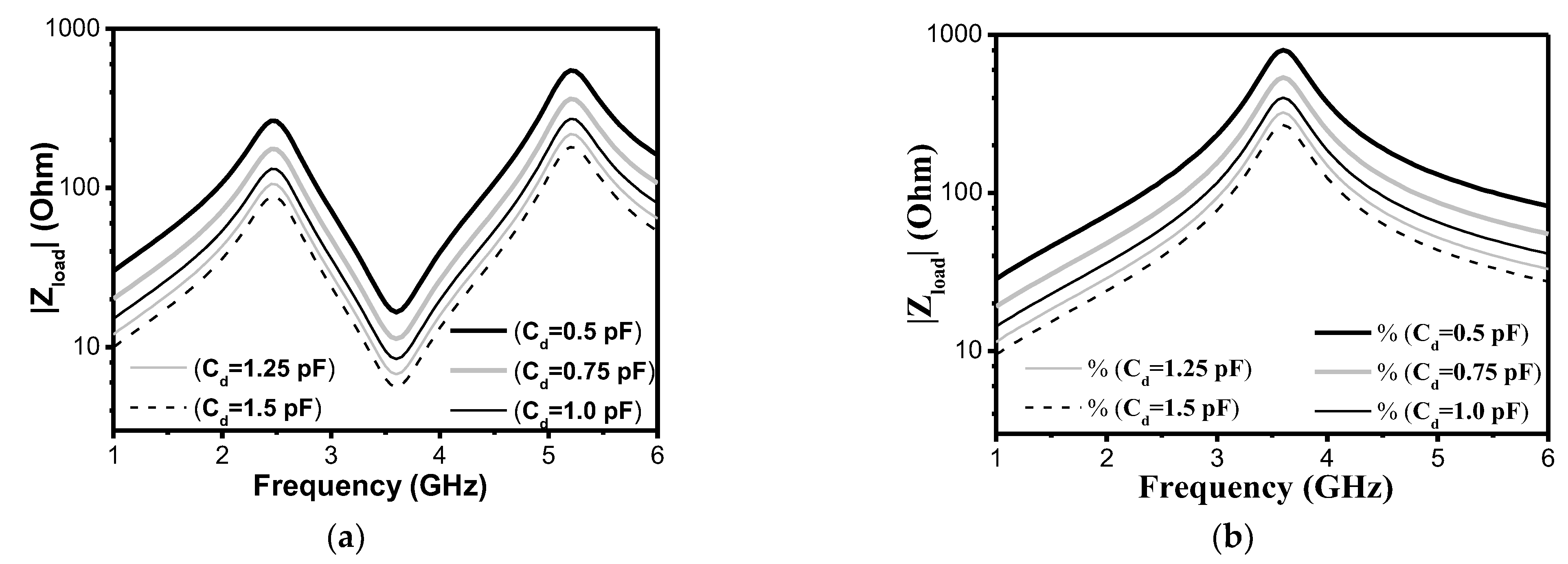
The proposed triple-band load network has three given target frequencies for the four load components, implying that there is one degree of freedom, say Cd, left for the circuit design. Figure 2 shows the load impedance versus frequency with different Cd parameters. As shown in Figure 2a, the dual-band network provides double-peak amplitudes of load impedance when the switch is on. Figure 2b shows the load impedance of a single-band network when the switch is off.
In general, the first step in the design criteria of the proposed load network is to select a lower Cd on account of the higher load impedance (i.e., the LNA gain). However, a drawback of the design is the high implementation cost due to the requirement of large inductance L1 and Ld. Therefore, the trade-off between the gain and die area should be considered [18].

2.2. Conventional Gyrator-Based Active Inductor and Proposed Gyrator-Based Triple-Band Input Matching Network

The conventional gyrator-based active inductor [18] is shown in Figure 3a. Transistors M1–M3 were employed to establish a back-to-back transconductor stage, where M1 is a common-drain stage, functioning as the feedback element, and M2–M3 comprise a cascode stage, which is the gain element. The transistor M3 is used as a gain booster. The inductive impedance in the Smith chart and the equivalent circuit comprising an inductor, capacitor, and resistor are shown in Figure 3b,c, respectively. The gyrator-based circuit topology can be simplified as shown in Figure 3d. In the proposed input matching network, the gyrator topology comprises a feedback (Gm1) and feedforward gain (Gm2) element to convert the capacitive impedance into inductive impedance. The impedance can be changed from capacitive Cx to inductive Lin [19] and can be derived as
I in = G m 2 ( G m 1 V i n × 1 s C X )
and
Z in = V in I in = s C X G m 1 × G m 2 = s L i n
In Equation (7), Zin is with an inductive loading Lin with an inductance Cx/(Gm1 × Gm2). The proposed input matching network is presented with an additional switched resonator ZL_sw between point X and Vdd. Therefore, we added a resonator ZL_sw parallel to the capacitor Cx (here, Zc = 1/sCx), as shown in Figure 3e. The impedance Zin can be written as
Z in = V in I in = 1 G m 1 × G m 2 ( Z c Z L _ s w )
Zin will be an inductive loading with an inductance Cx/(Gm1 × Gm2) if ZL_sw is merely an open loading.
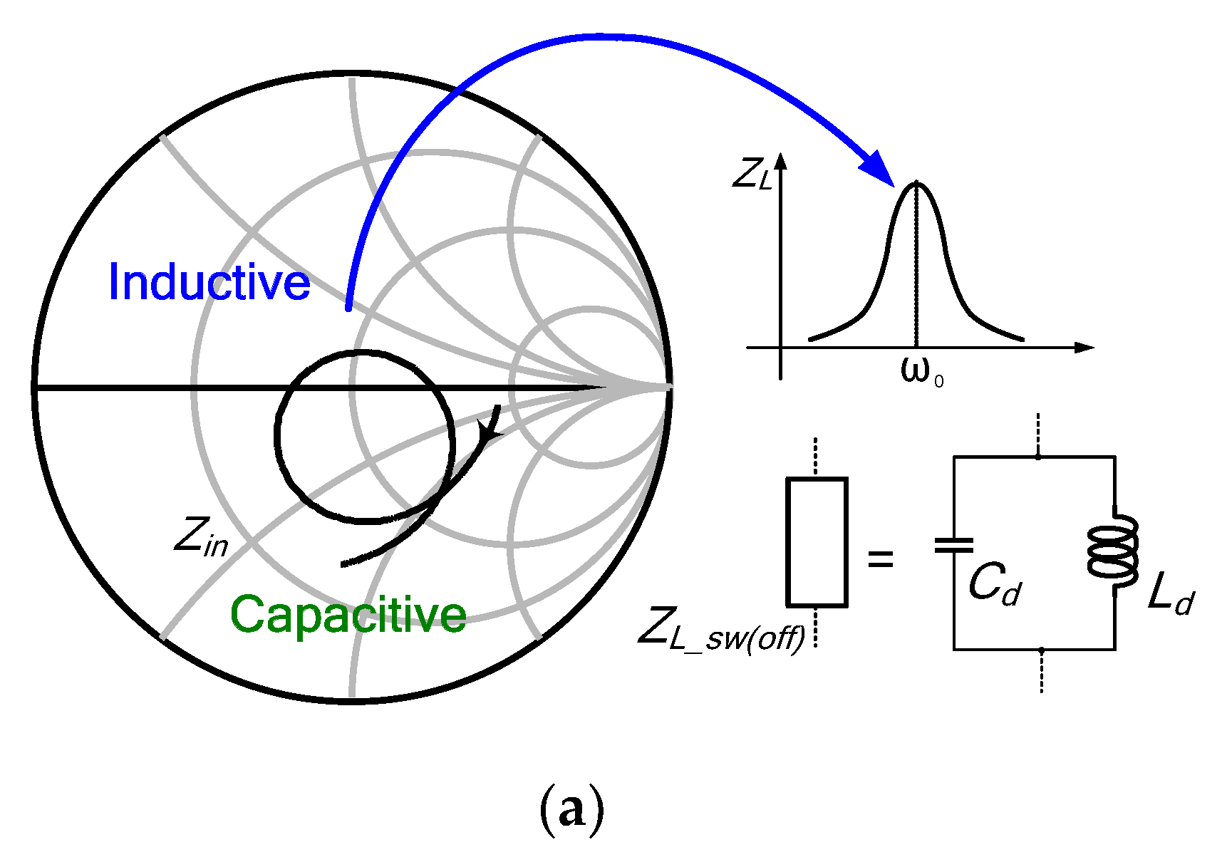
As shown in Figure 4a, with a gyrator-based design, Zin can be inductive around the resonant frequency ωo when the switch of ZL_sw is off. Contrarily, the impedance at the output node X is capacitive when the operating frequency is far from the resonant frequency. When the switch of ZL_sw is on, ZL_sw is changed to a dual resonator loading, as shown in Figure 4b, with dual inductive points found at the resonated frequencies ω1 and ω2. By contrast, the triple-band input matching network can be accomplished when the feedback mechanism is provided with the proposed switched resonator.

2.3. Noise Reduction with Large Substrate Resistance

Because the receiver sensitivity is determined by the thermal noise floor at input, the noise figure (NF) of the receiver, and the signal-to-noise ratio (SNR) requirement at the detector and NF of the receiver is dominated by the first stages of the receiver [20], a noise reduction technique with substrate resistor is applied to decrease the noise power of LNA.
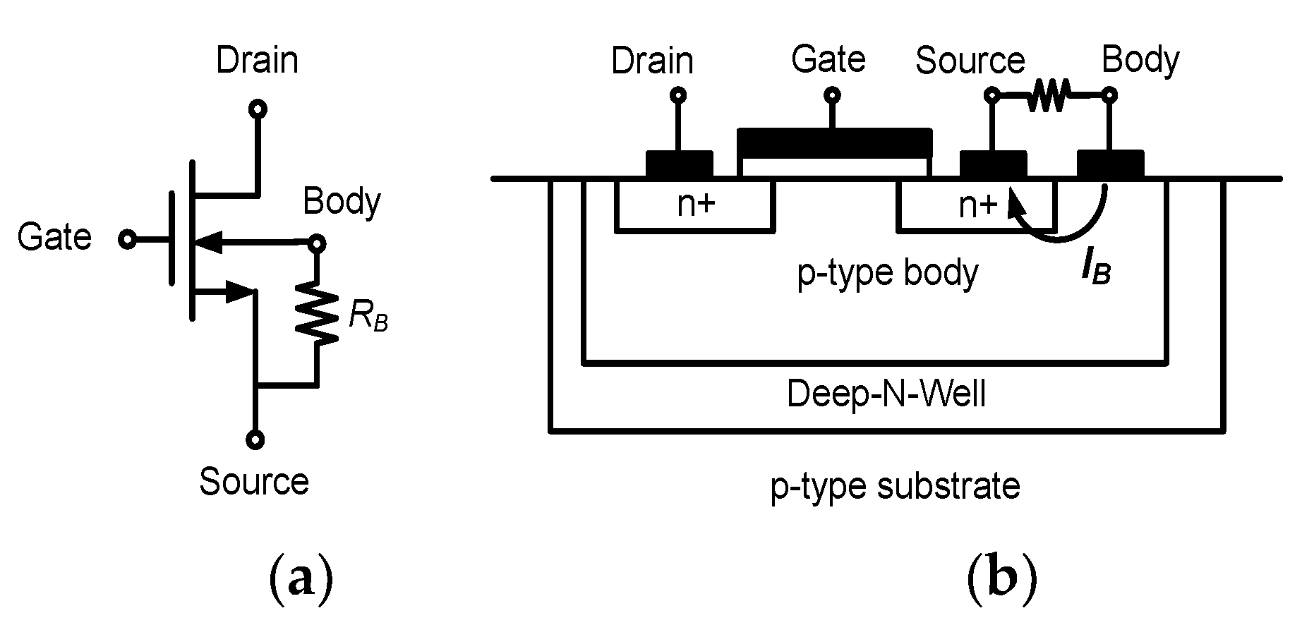
As shown in Figure 5a, RB is employed in an N-type Metal-Oxide-Semiconductor (NMOS) device to ameliorate the noise performance of the proposed CMOS LNA. The structure of a NMOS with RB is shown in Figure 5b. The NF can be derived as [21]
NF = NF min + G n R s × | Z s R o p t j X o p t | 2
Gn and NFmin can be written as
G n = K g ω 2 C g s 2 g m × ( 1 + R d R d s R s u b )
and
NF min = 1 + 2 G n ( R g + R s + R o p t )
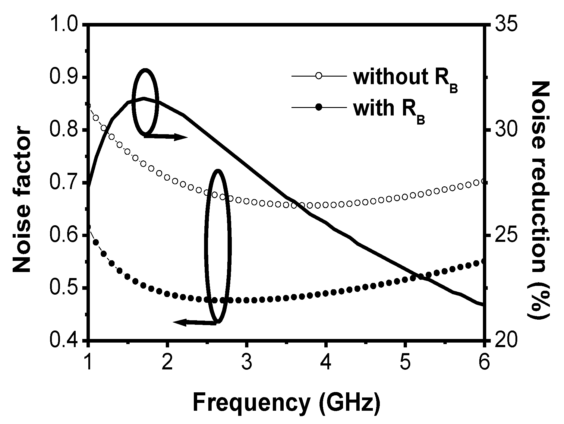
From (10) and (11), it can be observed that the increased resistance of the equivalent substrate resistor Rsub diminishes Gn, which in turn reduces the minimum noise figure NFmin. Furthermore, the NF can also be reduced by reducing Gn and NFmin in (9) [22]. Figure 6 presents the simulated noise factor F contributed by all MOSFET devices with and without RB. Note that the simulated VSB approaches zero, so the body-effect transconductance can be neglected [23].
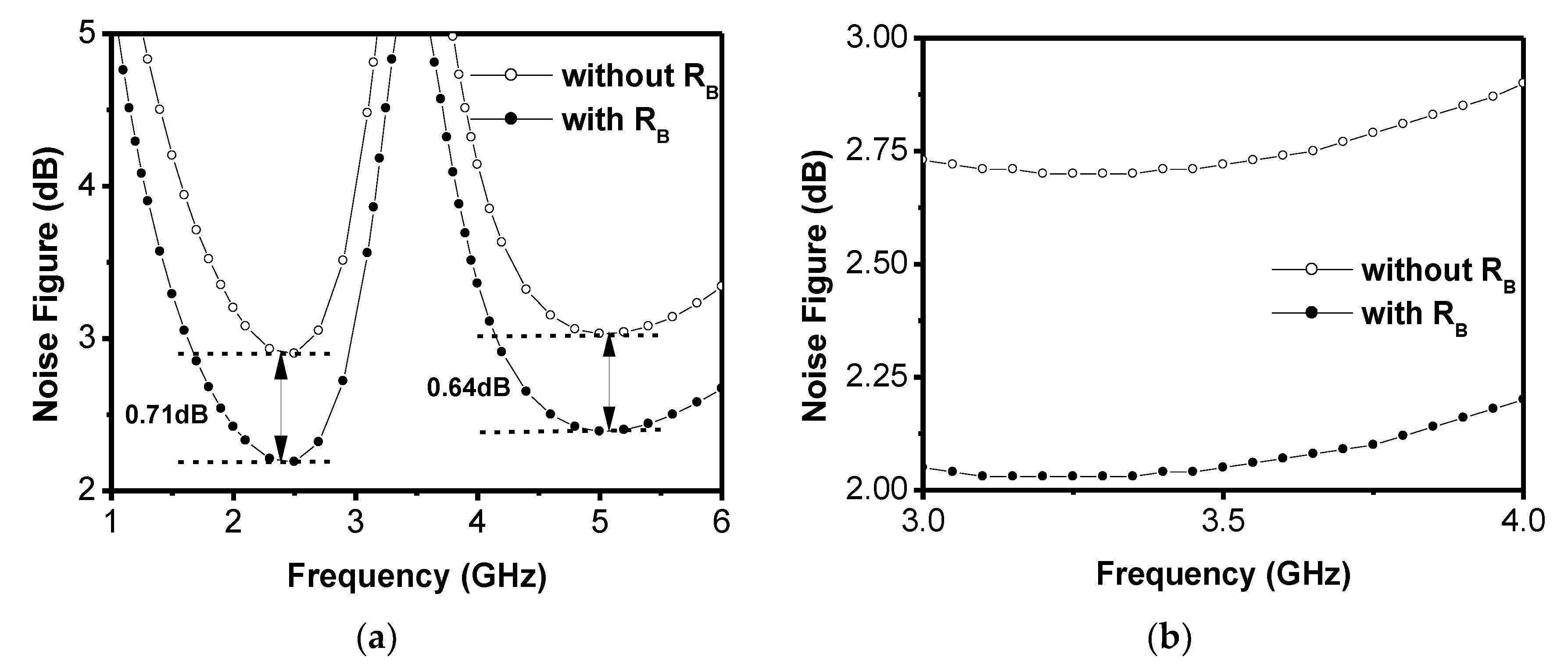
A larger Zsub by increasing the value of RB results in the reduction of the noise factor. The noise factor F contributed by the MOS device is shown in Figure 6, and a considerable noise power reduction in the MOS device can be demonstrated by the additional resistance RB. A maximum of 32% noise reduction can be achieved without requiring additional chip area and dc power because the size of the 8 kΩ High Resistance Implant (HRI) resistor is only 2 um × 15 um [22]. Figure 7 shows the simulation results of the noise figure with and without the additional resistance RB. A decrease of 0.71/0.67/0.64 dB noise figure was achieved at 2.5/3.5/5.2 GHz due to the usage of the larger resistance RB = 8 kΩ.

3. Proposed Switched Triple-Band LNA

To provide coverage for a wide range of wireless communication services, three spectrums will be covered with up to 400, 400, and 800 MHz from 2.3–2.7, 3.4–3.8, and 5.1–5.9 GHz, respectively, which include TD-LTE Band 40–41, Band 42–43, mid-band 5G, and the unlicensed 5-GHz band. To achieve 5 dB noise figure specifications [24], the 2 dB margin of the noise figure is appreciated when the effects of process, voltage, and temperature (PVT) variations can be estimated by simulation [25]. Consequently, the target noise figure of the proposed LNA is less than 3 dB with sufficient gain in 2-, 3-, and 5-GHz bands.
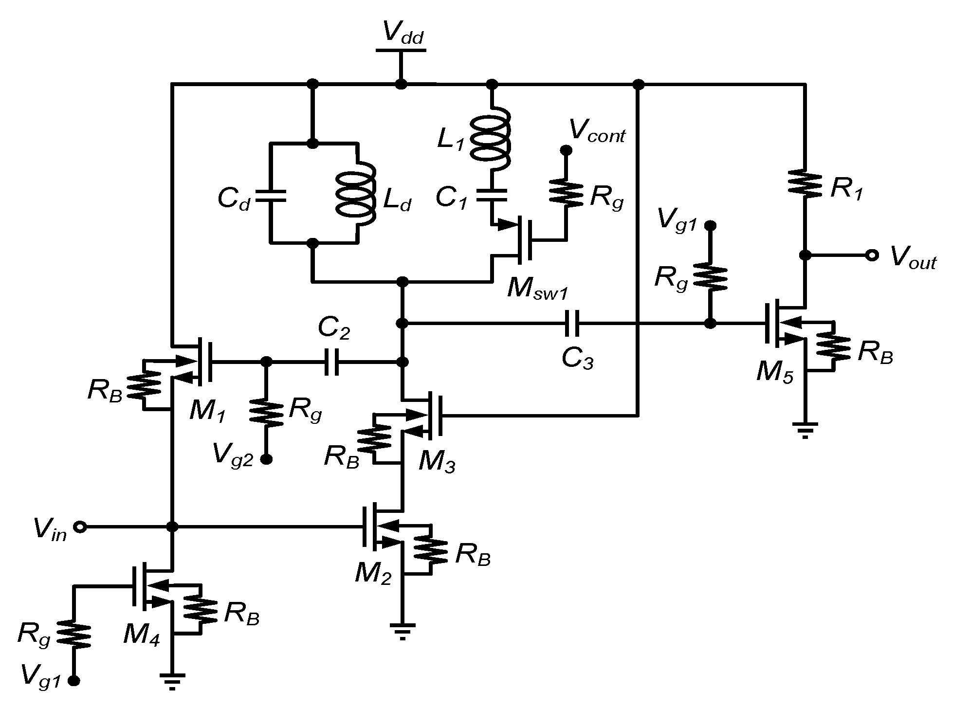
The triple-band LNA can reduce the chip area considerably by using a dual-band input network with an additional switched component. As shown in Figure 8, we designed the LNA to utilize a double-peak single-notch network with an additional switch as the load impedance to have the same characteristics of the input network. The additional resistance RB was adopted to simultaneously accomplish noise power reduction. The transistor M5 with a 50 Ω resistive load R1 was employed to achieve output matching for testing purposes. A decrease of 0.71/0.67/0.64 dB in the noise figure was attained at 2.5/3.5/5.2 GHz due to the use of RB.

4. Measurement Results

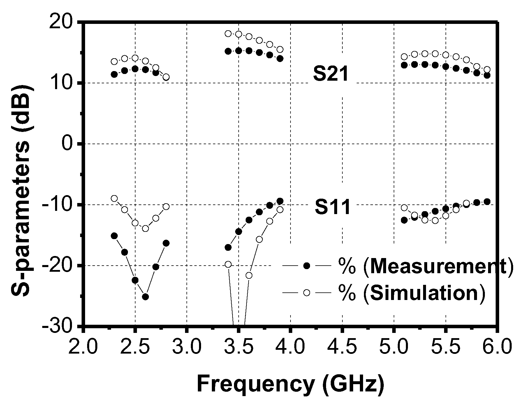
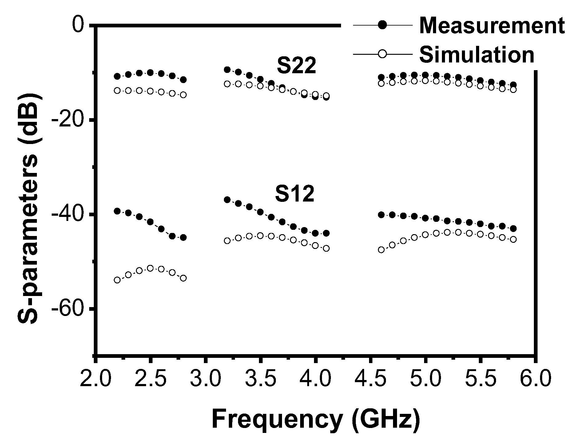
The LNA chip draws 7.9 mA dc core current from the 1.8 V supply voltage. The S parameters of the designed gain and input return loss are depicted in Figure 9 and Figure 10. The measured power gains at 2.5/3.5/5.2 GHz were 12.3/15.3/13.1 dB, and the input return losses were more than 10 dB among the three operating frequencies. The noise figure was measured using Agilent N8975A noise figure analyzer with Agilent 346C noise source. The simulated and measured noise figures at the same bias condition are depicted in Figure 11. The measured noise figures at 2.5/3.5/5.2 GHz were 2.3/2.2/2.6 dB. The relation between the input third-order intercept point (IIP3) and the 1-dB compression points (P1dB) is shown as [24].
IIP 3 = P 1 dB + 9.6   dB
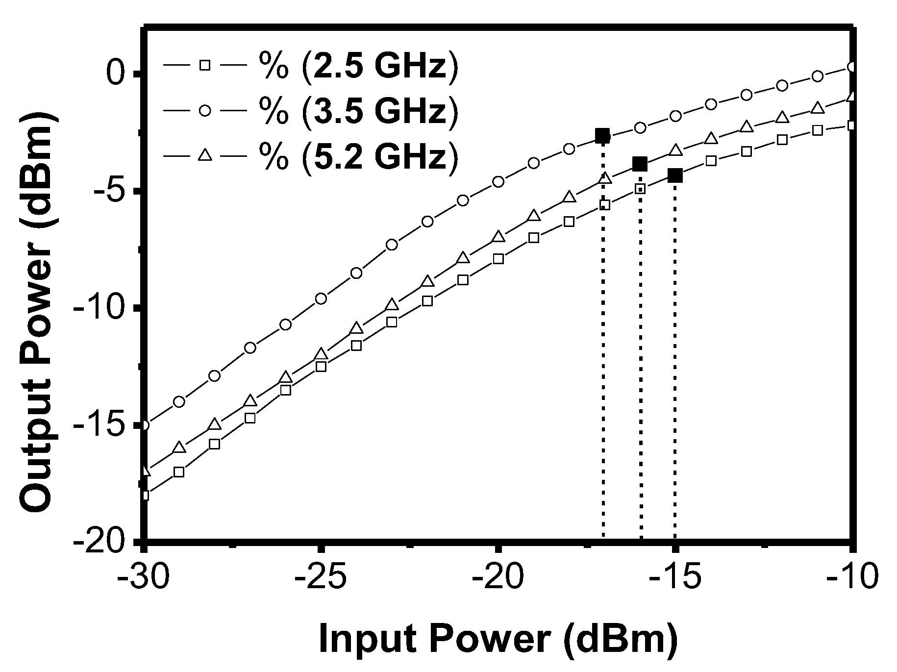
The measured P1dB are −15/−16/−17 dBm at 2.5/3.5/5.2 GHz, as shown in Figure 12, therefore, IIP3 could be calculated as −5.4/−6.4/−7.4 dBm.
The measurement results of the proposed LNA are summarized with recently published information in Table 1.
For performance comparison, the figure of merit (FOM) is defined by [31]:
FOM = Gain ( abs ) × IIP 3 ( mW ) × fc ( GHz ) ( NF 1 ) ( abs ) × Power consumption ( mW )
Comparing the performance among the three operating frequencies, in terms of power gain, noise figure, and cost, the proposed switched triple-band LNA is the only one that can cover the whole target bands and provide the lowest NFmin with adequate power gain among 2-, 3-, and 5-GHz frequencies. The measured power consumption of the proposed design is slightly large due to the additional buffer amplifier stage for testing purposes. In this study, the circuit simulation was performed using Agilent’s Advanced Design System (ADS) software with a TSMC design kit. In addition, the LNA is fabricated in an inexpensive 0.18-μm CMOS process with a smaller chip-size, therefore, it has an advantage in terms of lower manufacturing cost.

5. Conclusions

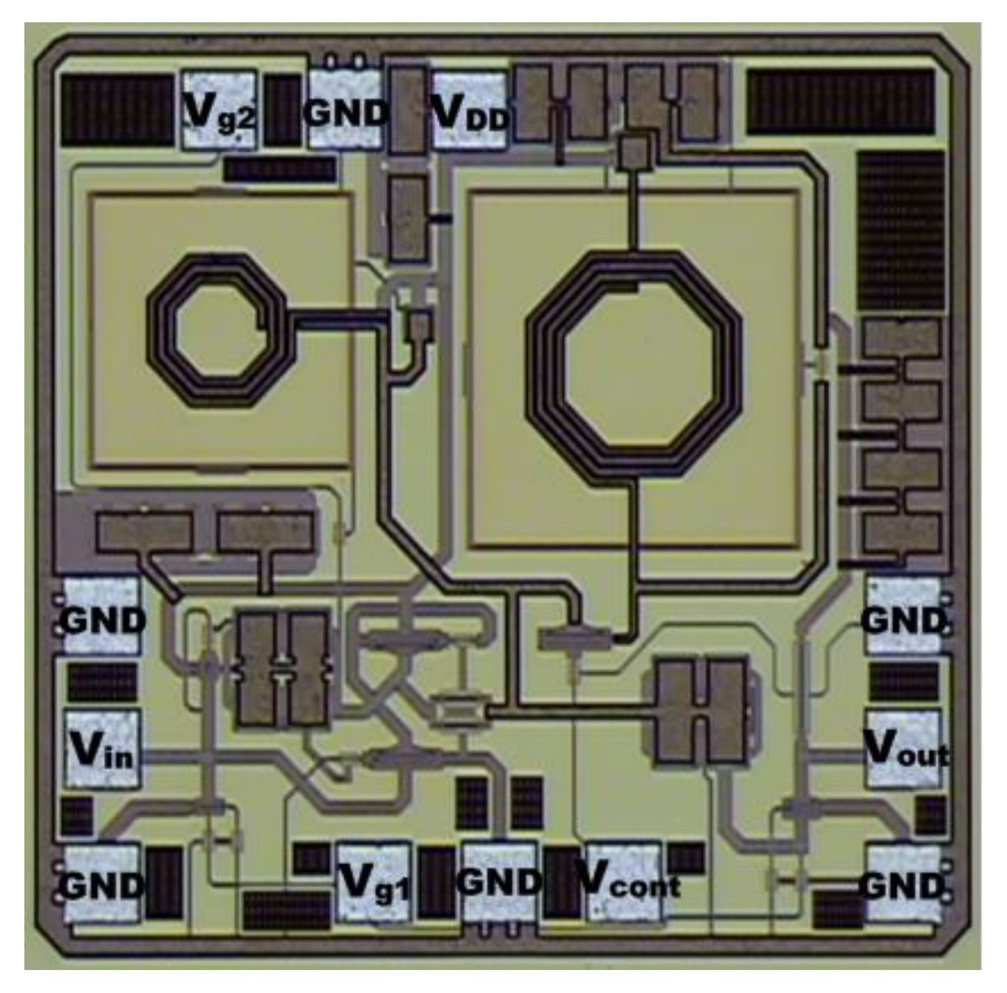
The die microphotograph of the fabricated LNA and the corresponding transistors and inductor sizes are shown in Figure 13, with the die area including pads of 0.75 × 0.69 mm2. The target frequencies of the proposed triple-band LNAs were 2.5, 3.5, and 5.2 GHz, which can be used in TD-LTE, mid-band 5G, LTE-U, and WLAN technology. A triple-band LNA with a switched resonator concept was fabricated using TSMC 0.18-μm CMOS technology, and a considerable die area reduction was achieved. Furthermore, an additional substrate resistance RB diminished the output noise power density of the MOS device, and a 0.71/0.67/0.64-dB decrease in the noise figure was attained at 2.5/3.5/5.2 GHz by using the triple-band LNA without additional chip area, dc power, and CMOS process steps. The frequency range for each band are 2.3–2.7, 3.4–3.8, and 5.1–5.9 GHz, including TD-LTE Band 40–41, Band 42–43, mid-band 5G, and the unlicensed 5-GHz band operation. The measured 10 dB return loss can be achieved to fulfil triple-band operation with moderate gain around 12 dB, and 2.2~2.7 dB noise figure. The measurement result agrees well with the simulation result.

Author Contributions

The study was performed by authors as follows: Conceptualization: C.-H.T. and C.-Y.L.; methodology: C.-H.T. and C.-Y.L.; validation: C.-Y.L.; formal analysis: C.-H.T. and C.-Y.L.; investigation: C.-H.T. and C.-Y.L.; writing—original draft preparation: C.-H.T. and C.-Y.L.; writing—review and editing: C.-H.T.; visualization: C.-H.T. and C.-Y.L.; supervision: C.-P.L., S.-J.C. and J.-H.T. All authors have read and agreed to the published version of the manuscript.

Funding

This research received no external funding.

Institutional Review Board Statement

Not applicable.

Informed Consent Statement

Not applicable.

Data Availability Statement

Not applicable.

Acknowledgments

This work was supported by the National Science Council of Taiwan, Republic of China, under contract NSC96-2752-E009-003-PAE. The authors thank the National Chip Implementation Center (CIC), Taiwan, for their help in chip fabrication.

Conflicts of Interest

The authors declare no conflict of interest.

References

  1. 4G Wireless Broadband Industry White Paper. Available online: http://lte-tdd.org/d/file/Resources/rep/2017-03-01/00c1864037fd2e95525cc46da3919e99.pdf (accessed on 1 March 2017).
  2. Ye, Y.; Wu, D.; Shu, Z.; Qian, Y. Overview of LTE spectrum sharing technologies. IEEE Access 2016, 4, 8105–8115. [Google Scholar] [CrossRef]
  3. 5G Deployment: State of Play in Europe, USA and Asia. Available online: https://www.europarl.europa.eu/RegData/etudes/IDAN/2019/631060/IPOL_IDA(2019)631060_EN.pdf (accessed on 30 April 2019).
  4. Wang, H.; Zhang, R.; Luo, Y.; Yang, G. Compact eight-element antenna array for triple-band MIMO operation in 5G mobile terminals. IEEE Access 2020, 8, 19433–19449. [Google Scholar] [CrossRef]
  5. Wang, X.; Quek, T.Q.S.; Sheng, M.; Li, J. Throughput and fairness analysis of Wi-Fi and LTE-U in unlicensed band. IEEE J. Sel. Areas Commun. 2017, 35, 63–78. [Google Scholar] [CrossRef]
  6. Hamidouche, K.; Saad, W.; Debbah, M. A multi-game framework for harmonized LTE-U and WiFi coexistence over unlicensed bands. IEEE Trans. Wirel. Commun. 2016, 23, 62–69. [Google Scholar] [CrossRef]
  7. Maksymyuk, T.; Kyryk, M.; Jo, M. Comprehensive spectrum management for heterogeneous networks in LTE-U. IEEE Trans. Wirel. Commun. 2016, 23, 8–15. [Google Scholar] [CrossRef]
  8. IEEE 802.11. Available online: https://www.ieee802.org/11 (accessed on 2 February 2021).
  9. Ingels, M.; Giannini, V.; Borremans, J.; Mandal, G.; Debaillie, B.; Van Wesemael, P.; Sano, T.; Yamamoto, T.; Hauspie, D.; Van Driessche, J.; et al. A 5 mm2 40 nm LP CMOS transceiver for a software-defined radio platform. IEEE J. Solid-State Circuits 2010, 45, 2794–2806. [Google Scholar] [CrossRef]
  10. Xie, H.; Rakers, P.; Fernandez, R.; McCain, T.; Xiang, J.; Parkers, J.; Riches, J.; Verellen, R.; Rahman, M.; Shimoni, E.; et al. Single-chip multiband EGPRS and SAW-less LTE WCDMA CMOS receiver with diversity. IEEE Trans. Microw. Theory Techn. 2012, 60, 1390–1396. [Google Scholar] [CrossRef]
  11. Analui, B.; Mercer, T.; Mandegaran, S.; Goel, A.; Hashemi, H. A 50 MHz–6 GHz, 2 × 2 MIMO, Reconfigurable Architecture, Software-defined Radio in 130 nm CMOS. In Proceedings of the IEEE Radio Frequency Integrated Circuits Symposium, Tampa, FL, USA, 1–3 June 2014; pp. 329–332. [Google Scholar]
  12. Vauche, R.; Muhr, E.; Fourquin, O.; Bourdel, S.; Gaubert, J.; Dehaese, N.; Meillere, S.; Barthelemy, H.; Ouvry, L. A 100 MHz PRF IR-UWB CMOS transceiver with pulse shaping capabilities and peak voltage detector. IEEE Trans. Circuits Syst. I Regul. Pap. 2017, 64, 1612–1625. [Google Scholar] [CrossRef]
  13. Neihart, N.M.; Brown, J.; Yu, X. A dual-band 2.45/6 GHz CMOS LNA utilizing a dual-resonant transformer-based matching network. IEEE Trans. Circuits Syst. I Reg. Pap. 2012, 59, 1743–1751. [Google Scholar] [CrossRef]
  14. Ye, R.F.; Horng, T.S.; Wu, J.M. Low-noise and high-linearity wideband CMOS receiver front-end stacked with glass integrated passive devices. IEEE Trans. Microw. Theory Tech. 2014, 62, 1229–1238. [Google Scholar] [CrossRef] [Green Version]
  15. Chen, C.C.; Lin, Y.S.; Huang, P.L.; Chang, J.F.; Lu, S.S. A 4.9-dB NF 53.5-62-GHz micro-machined CMOS wideband LNA with small group-delay-variation. In Proceedings of the IEEE MTT-S International Microwave Symposium Digital, Anaheim, CA, USA, 23–28 May 2010; pp. 489–492. [Google Scholar]
  16. LTE TDD—The Global Solution for Unpaired Spectrum. Available online: https://www.qualcomm.com/documents/lte-tdd-global-solution-unpaired-spectrum (accessed on 19 August 2013).
  17. Catherwood, P.A.; Black, B.; Mohamed, E.B.; Cheema, A.A.; Rafferty, J.; Mclaughlin, J.A.D. Radio channel characterization of mid-band 5G service delivery for ultra-low altitude aerial base stations. IEEE Access 2019, 7, 8105–8115. [Google Scholar] [CrossRef]
  18. Lin, C.Y.; Li, W.T.; Liang, C.P.; Chung, S.J. An active triple band-notched filter with improved Q-factor for UWB system. In Proceedings of the Asia-Pacific Microwave Conference 2011, Melbourne, VIC, Australia, 5–8 December 2011. [Google Scholar]
  19. Thanachayanont, A.; Payne, A. VHF CMOS integrated active inductor. IET Electron. Lett. 1996, 32, 999–1000. [Google Scholar] [CrossRef]
  20. Gu, Q. RF System Design of Transceivers for Wireless Communications; Springer: New York, NY, USA, 2005. [Google Scholar]
  21. Lin, Y.S. An analysis of small-signal source-body resistance effect on RF MOSFETs for low-cost system-on-chip (SoC) applications. IEEE Trans. Electron. Devices 2005, 52, 1442–1451. [Google Scholar] [CrossRef]
  22. Lee, J.Y.; Park, H.K.; Chang, H.J.; Yun, T.Y. Low-power UWB LNA with common-gate and current reuse techniques. IET Microw. Antennas Propag. 2012, 6, 793–799. [Google Scholar] [CrossRef]
  23. Lin, C.Y.; Liang, C.P.; Tarng, J.H.; Chung, S.J. Compact composite noise-reduction LNA for UWB WPAN and WBAN applications. IET Map 2018, 12, 903–908. [Google Scholar] [CrossRef]
  24. LTE. Evolved Universal Terrestrial Radio Access (EUTRA); Radio Frequency (RF) Requirements for LTE Pico Node B. ETSI TR 136 931 v14.0.0. 2017. Available online: https://www.etsi.org/deliver/etsi_tr/136900_136999/136931/14.00.00_60/tr_136931v140000p.pdf (accessed on 2 February 2021).
  25. Jayaraman, K.; Khan, Q.; Chi, B.; Beattie, W.; Wang, Z.; Chiang, P. A self-healing 2.4 GHz LNA with on-chip S11/S21 measurement/calibration for in-situ PVT compensation. In Proceedings of the IEEE Radio Frequency Integrated Circuits Symposium, Anaheim, CA, USA, 23–25 May 2010; pp. 311–314. [Google Scholar]
  26. Razavi, B. RF Microelectronics; Prentice-Hall: Upper Saddle River, NJ, USA, 2012. [Google Scholar]
  27. Adom-Bamfi, G.; Entesari, K. A multiband low noise amplifier with a switchable Gm active shunt feedback for SDRs. In Proceedings of the IEEE Radio and Wireless Symposium, Austin, TX, USA, 24–27 January 2016; pp. 179–182. [Google Scholar]
  28. Fu, C.T.; Ko, C.L.; Kuo, C.N.; Juang, Y.Z. A 2.4–5.4-GHz wide tuning-range CMOS reconfigurable low-noise amplifier. IEEE Trans. Microw. Theory Techn. 2008, 56, 2754–2763. [Google Scholar]
  29. Yu, X.; Neihart, N.M. Analysis and design of a reconfigurable multimode low-noise amplifier utilizing a multitap transformer. IEEE Trans. Microw. Theory Techn. 2013, 61, 1236–1246. [Google Scholar] [CrossRef]
  30. Lim, K.; Min, S.; Lee, S.; Park, J.; Kang, K.; Shin, H.; Shim, H.; Oh, S.; Kim, S.; Lee, J.; et al. A 2 × 2 MIMO tri-band dual-mode direct-conversion CMOS transceiver for worldwide WiMAX/WLAN applications. IEEE J. Solid-State Circuits 2011, 46, 1648–1658. [Google Scholar] [CrossRef]
  31. Taibi, A.; Slimane, A.; Belaroussi, M.T.; Tedjini, S.A.; Trabelsi, M. Low power and high linear reconfigurable CMOS LNA for multi-standard wireless applications. In Proceedings of the 2013 25th International Conference on Microelectronics (ICM), Beirut, Lebanon, 15–18 December 2013. [Google Scholar]
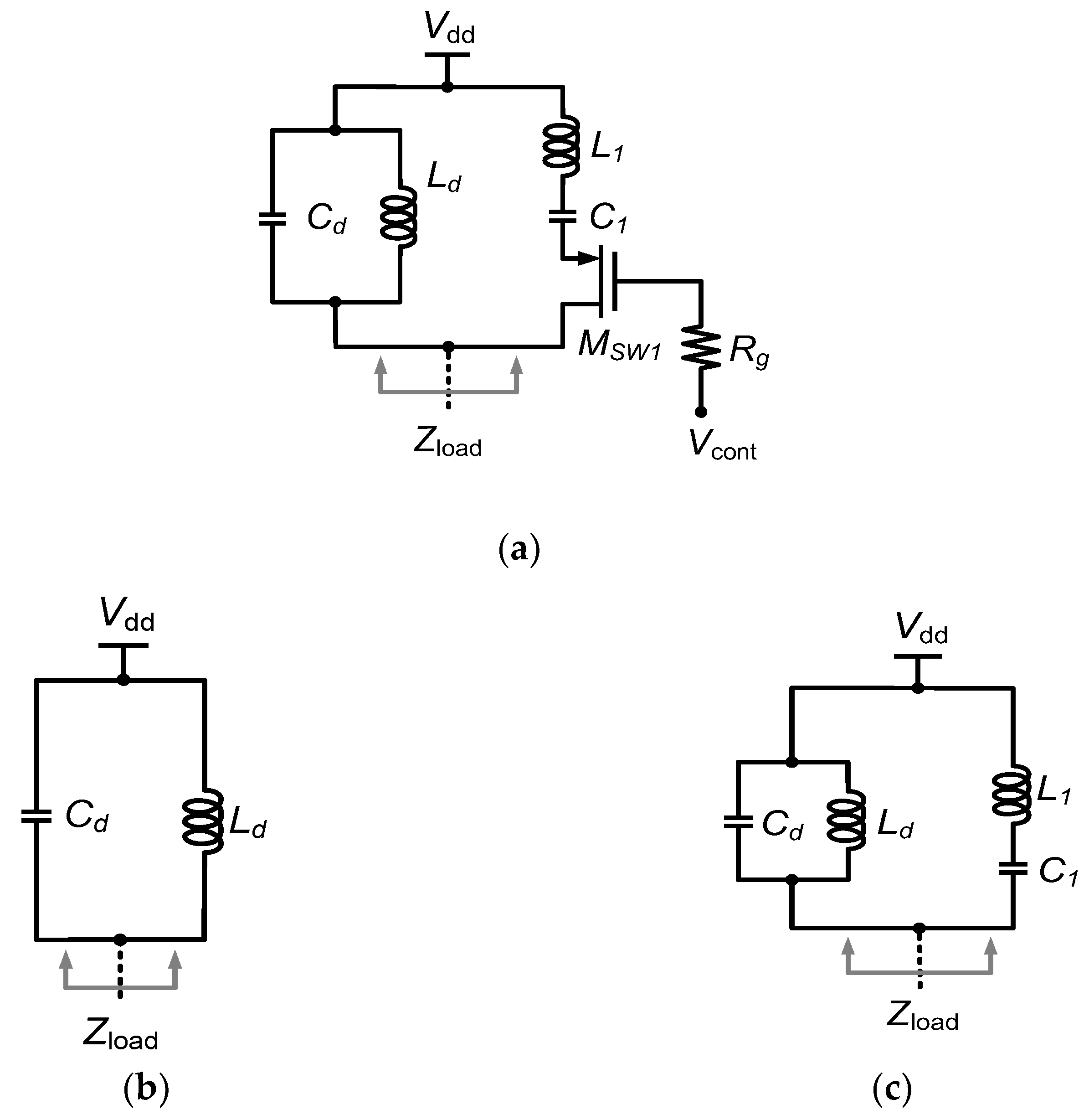
Figure 1. Schematic of the load network. (a) The proposed triple-band load network with an additional switched component, (b) single-band network, (c) and dual-band network.
Applsci 11 01477 g001
Figure 2. Load impedance versus frequency with different Cd parameters. (a) A dual-band load network when the switch is on. (b) A single-band load network when the switch is off.
Applsci 11 01477 g002
Figure 3. Conventional and proposed gyrator-based topology. (a) Schematic of regulated cascode active inductor, (b) Smith chart, (c) equivalent circuit, (d) circuit topology and input impedance, (e) proposed gyrator-based circuit topology and its impedance with a switched resonator ZL_SW.
Applsci 11 01477 g003
Figure 4. Principle of the input matching technique. (a) Smith chart when the switch is off, (b) Smith chart when the switch is on.
Applsci 11 01477 g004aApplsci 11 01477 g004b
Figure 5. Additional larger substrate resistance RB. (a) A NMOS device with a larger substrate resistance RB = 8 kΩ, (b) structure of a NMOS with RB, (c) noise equivalent circuit of a NMOS device with RB.
Applsci 11 01477 g005aApplsci 11 01477 g005b
Figure 6. Simulated RF MOSFET noise factor F (NF = 10log10 (1 + F)) and noise reduction with and without RB.
Applsci 11 01477 g006
Figure 7. Simulated noise figure with and without the additional resistance RB = 8 kΩ. (a) Dual band when the switch is on, (b) single band when the switch is off.
Applsci 11 01477 g007
Figure 8. The proposed triple-band low-noise amplifier (LNA) with the load network design and the noise reduction resistor, the component values RB = 8 kΩ, Rg = 5.2 kΩ, R1 = 50 Ω, C1 = 588 fF, C2 = 3.8 pF, C3 = 3.8 pF, Cd = 388 fF.
Applsci 11 01477 g008
Figure 9. Measured and simulated S-parameters (S21 and S11) of the proposed LNA.
Applsci 11 01477 g009
Figure 10. Measured and simulated S-parameters (S22 and S12) of the proposed LNA.
Applsci 11 01477 g010
Figure 11. Measured and simulated noise figures of the proposed LNA.
Applsci 11 01477 g011
Figure 12. The linearity (P1dB) of the proposed LNA.
Applsci 11 01477 g012
Figure 13. Microphotograph of the proposed LNA with 0.75 × 0.69 mm2 die area with transistor sizes W/L (μm) M1 = 30/0.18, M2 = 320/0.18, M3 = 320/0.18, M4 = 18/0.5, M5 = 125/0.18, Msw1 = 384/0.18, and inductor sizes width/turns/radius of spiral L1 = 6 μm/3/39 μm, L2 = 6 μm/3.5/61 μm.
Applsci 11 01477 g013
Table 1. Performance summary of the published CMOS LNAs.
Ref.TechnologyFreq. (GHz)Gmax (dB)NFmin (dB)IIP3 (dBm)Power Consumption (mW)FOM 5Area (mm2)
[26]0.18-μm2.414.43.3−7.127.21.660.63
3.5133.8−6.2
5.2 1104.3−4.34
[27]0.13-μm2.422.12.8−18.24.66.010.49
3.422.62.2−15.3
5.4 124.83.1−20.4
[28]0.13-μm2.8 216.12.4−46.49.610.44
3.314.23.0−2
5.6514.94.8−4.2
[29]0.13-μm2.4152.7−12- 6- 6- 6
3.5−13.5
5.2−13
[30]0.18-μm2.4–1114.84.1−11.53.41.721.1 4
[22]0.18-μm2.3–4.827 32.7 3−3.2 313.1260.34
This work0.18-μm2.512.32.3−5.414.22.90.52
3.515.32.2−6.4
5.213.12.7−7.4
1 5 GHz band provides less than 800 MHz. 2 2 GHz band lacks for time-division long-term evolution (TD-LTE) Band 40. 3 Simulation result. 4 Chip area is the largest in Table 1. 5 Only the best result for all operating bands is shown. 6 Full TRX design. IIP3: input third-order intercept point; FOM: figure of merit.
Publisher’s Note: MDPI stays neutral with regard to jurisdictional claims in published maps and institutional affiliations.