Article

Comparison of Nondestructive Testing Methods for Solder, Sinter, and Adhesive Interconnects in Power and Opto-Electronics

Institute of Innovative Mobility (IIMo), Technische Hochschule Ingolstadt, 85049 Ingolstadt, Germany
*
Author to whom correspondence should be addressed.
Appl. Sci. 2020, 10(23), 8516; https://doi.org/10.3390/app10238516
Submission received: 30 October 2020 / Revised: 24 November 2020 / Accepted: 25 November 2020 / Published: 28 November 2020
(This article belongs to the Special Issue Nondestructive Testing (NDT): Volume II)

Abstract

:
Reliability is one of the major requirements for power and opto-electronic devices across all segments. High operation temperature and/or high thermomechanical stress cause defects and degradation of materials and interconnects, which may lead to malfunctions with costly or even life-threatening consequences. To avoid or at least reduce failures, nondestructive testing (NDT) methods are common within development and production of power and opto-electronics. Currently, the dominating NDT methods are X-ray, scanning acoustic microscopy (SAM), and transient thermal analysis (TTA). However, they have different strengths and weaknesses with respect to materials and mechanical designs. This paper compares these NDT methods for different interconnect technologies, i.e., reflow soldering, adhesive, and sintered interconnection. While X-ray provided adequate results for soldered interfaces, inspection of adhesives and sintered interconnects was not possible. With SAM, evaluation of adhesives and sintered interconnects was also feasible, but quality depended strongly on the sample under test. TTA enabled sufficiently detailed results for all the interconnect applications. Automated TTA equipment, as the in-house developed tester used within this investigation, enabled measurement times compatible with SAM and X-ray. In the investigations, all methods revealed their pros and cons, and their selection has to depend on the sample under tests and the required analysis depth and data details. In the paper, guidelines are formulated for an appropriate decision on the NDT method depending on sample and requirements.

1. Introduction

The strongly growing markets of power electronics [1] and opto-electronics, e.g., laser modules and solid-state lighting (SSL) [2], share the same problem of high thermal losses across small areas, which have to be reliably dissipated to avoid lifetime-reducing overtemperatures. For power electronics, most crucial components are switches (e.g., metal oxide semiconductor field effect transistors (MOSFETs) and insulated gate bipolar transistors (IGBTs)) and diodes [3], generating power losses in the form of heat due to switching and conductive losses. In SSL, critical components are laser diodes and power-LEDs (referred to as just LED in the following) with limited efficiency while converting electrical to optical power. As different as both electronic segments may be, the semiconductors are the most critical components, and the concept of heat management is also similar.
The concept is described in Figure 1 in a general manner and is used for most (a) power electronics and (b) SSL applications. Heat is induced at the junction of the semiconductor and transferred downward through the chip to the large-area interconnect 1, which is responsible for not only electrical but also thermal connection. Typical for interconnect 1 is soldering or sintering. A distinction can be made between single electrical contact interconnects (die bonds), e.g., for bare die chips with wire bonds to realize all other electrical connections in (a), and multi electrical contact interconnects, e.g., for packaged LEDs where all electrical contacts are realized by large-area solder pads with small gaps in between on the backside in (b). From interconnect 1, the heat flows through the substrate, realizing an electrical circuit with copper structures and traces. For thermally critical applications, mostly direct bonded copper (DBC) substrates (set-up: 0.15–0.8 mm copper/0.25–1.0 mm ceramic/0.15–0.8 mm copper) [4] or insulated metal substrate printed circuit boards (IMS-PCB) (set-up: 0.018–0.105 mm copper, 0.05–0.2 mm deictic, 0.3–3.0 mm aluminum or copper core) [5] are used. Inside the substrate, the heat is spread in the horizontal direction, reducing the thermal resistance by increasing the heat transfer cross-section. The substrate is attached with the full-area interconnect 2 to the heat sink, where the heat is passively, e.g., via convection of cooling fins, or actively, e.g., via forced convection by fans or liquid cooling, dissipated to the ambient. Typical for interconnect 2 are soldered and adhesive interconnects or thermal interface materials (TIM). In some applications, an additional metal base plate is used between the substrate and heat sink to increase thermal mass and improve mechanical stability [6].
For good thermal performance and long lifetimes of new power electronics or SSL products, the thermal concept must be verified by calculations and simulations in the development process to keep the maximal operation temperature of the semiconductors within a noncritical range. However, due to production failures (e.g., incomplete printing or dispensing, improper component placement, contamination and volatile process parameters) or material degradation over years in operation (e.g., cracks and delamination), the thermal performance might be reduced. To avoid or at least minimize thermal failures, manufacturers use different nondestructive testing methods (NDTs) for qualification. Most popular and well established in power electronics and SLL development and production is X-ray inspection to detect inhomogeneities in metal structures, e.g., voids and nonwetted areas in soldered interconnects [7], even at production speed, allowing for in-line automated inspection. However, X-ray is limited for sintered interconnects and adhesives, since porosity of sintered interconnects is too small for the resolution of X-ray images [8], and adhesives have a very low density for detection between the surrounding high-density metal components [9]. Using scanning acoustic microscopy (SAM) instead, defects of sintered and adhesive interconnects can be detected. However, the modules have to be placed in water as couplant for the inspection, requiring an additional drying process. Furthermore, complex surface shapes (e.g., ribbon bonds) disturb evaluation. Transient thermal analysis (TTA) directly inspects the thermal behavior while heating up and cooling down of the module and could be a useful alternative; however, the long measurement time and the lack of an automatized equipment prohibit high-volume inspections. Through the use of an in-house developed automatized TTA equipment and measurement algorithm [10,11,12], the manual effort is drastically reduced and high-volume inspections are possible.
Altogether, each of the abovementioned NDTs for investigation shows advantages and drawbacks in applicability, effort, and data quality, whereas none is perfectly suitable to cover all requirements. This paper compares them on soldered, sintered, and adhesive interconnects to reveal differences and possibilities to facilitate a selection for different applications and thermomechanical set-ups.

2. Interconnect Technologies in Power Electronics and SSL

2.1. Soldering

Soldering is the most dominant interconnect technology in electronics production due to the simple processing for mass production. The standard solder paste application method is a stencil-printing process of viscous solder paste over a thin metal stencil onto the substrate. The solder paste consists of small metal spheres and a binder material including flux. Components are placed by an automatic pick and place machine into the printed solder reservoirs, and the assembled substrates are carried through a reflow oven with multiple temperature sections to fulfill an optimal solder profile for the paste. The soldering profile can be separated into the three processing zones, namely, preheat/soak (outgassing of binders and oxide reduction from the solder spheres by flux), reflow (solder is liquid), and cool down (solder solidifies). To increase the quality of solder interfaces, protection atmospheres, e.g., nitrogen gas, can additionally be used, or a vacuum can be applied [13,14].
A common issue in soldering is gas inclusion in the solder interconnect, referred to as voids. Voids reduce the cross-section for heat transfer and, therefore, have to be capped under a certain limit to be unproblematic [15]. By applying vacuum while the solder is liquid, most of the voids can be sucked out of the solder joint. More critical than voids are nonwetted areas due to residues on substrate or component pads, drastically reducing the contact area for electrical and thermal transfer. Reasons for residues can be contamination or inadequate handling of substrate and component or inappropriate process parameters [16]. A third issue involves cracks in the solder interconnect induced by a CTE mismatch (coefficient of thermal expansion) of component and substrate. Several cycles of heating and cooling over the operating lifecycle of the device slowly damage the solder interconnect leading to the growth of thin cracks. Heat and current transfer are no longer possible through these cracked areas and the thermal performance is reduced [17], until the interconnects finally fail electrically due to an open contact.

2.2. Sintering

Particle sintering has emerged as a reliable alternative to soldering in recent years for high-temperature applications [18]. Sintering is a mass transport phenomenon driven by the reduction in surface energy [16] and can be classified into three main stages: an initial stage defined by the formation of necks between the particles in contact, an intermediate stage defined by the formation of interconnected pores and the onset of grain growth, and a final stage defined by the development of isolated pores, thereby removing any hindrance to grain growth. Therefore, sintering as an advanced packaging solution helps in realizing an interconnect at relatively low temperature (<300 °C) but with a near-bulk-like microstructure characterized by finely dispersed micro and nanopores. A silver/copper sintered interconnect, hence, provides thermal, electrical, and mechanical properties far superior to any of the standard solder materials and offers a high operating temperature range (>200 °C).
Silver sintering under pressure has been industrialized for many applications in the power electronics sector [19], and copper sintering is being actively researched as a reliable low-cost alternative to silver sintering [20]. Stencil/screen printing, dispensing, and direct transfer film are some of the standard techniques used in the industry for die-attach applications using sinter pastes. Apart from the direct transfer film technique, a standard die-attach bonding sintering process involves the application of the sintering paste, a predrying step to remove excess volatile binder from the formation, and finally placement of the die and isothermal sintering under pressure. Pressureless sintering has also been suggested as an alternative process; however, reliability issues are a challenge to large-scale industrialization [21].
One of the most frequently observed defects with sintering is delaminations. These could occur due to contamination of the bonding surfaces, an insufficient/ineffective predrying process in the case of sintering under pressure, and/or improper application of bonding force during sintering among other factors, affecting the thermal path and, thus, the performance of the interconnect. Furthermore, the sintered interconnect reveals a porous microstructure characterized by finely dispersed micro and nanopores, where less porous structures lead to better thermal performance.

2.3. Adhesive

Different kinds of adhesives are used in the electronic industry to fulfill mechanical, electrical, and thermal tasks. They are based on organic materials containing small amounts of additive materials and can be basically separated into two classes: electrically conductive and nonconductive. Typical applications for adhesives are underfills for flip chips to improve reliability or chip attachment to flexible substrates [9,22]. Moreover, for die attach, adhesives are gaining importance [23,24]. However, this paper focuses on nonconductive adhesives for large-area attachments such as the attachment of substrates to a heat sink or base plate used in power electronics and SSL. While processing, the adhesive is applied in a fluid uncured state to the heat sink by dispensing, followed by pressing the substrate on the dispensed adhesive to squeeze it uniformly and achieve a homogeneous distribution. Afterward, the adhesive is cured in a thermal treatment similar to reflow soldering but with much lower temperatures (<200 °C).
Possible adhesive failures in production are tilting of the substrate (foreign object in adhesive layer), inadequate adhesive distribution (to less pressure for squeezing), missing adhesive (plugged dispense capillary), adhesive degradation (incorrect handling of adhesive while storage or mixing), and incomplete curing (incorrect curing parameters). All of them result in a decrease in thermal and mechanical performance [25].

3. Nondestructive Testing Methods

3.1. X-ray

High-frequency electromagnetic radiation in the range of 3 × 10¹⁶ to 3 × 10¹⁹ Hz is used for X-ray inspection. The high-energy photons are generated by an X-ray tube and are directed toward the specimen as the fanned beam of a point source, penetrate it, and are collected on the other side by a X-ray detector similar to a photo imaging sensor. Frequency and corresponding wavelength can be adjusted by varying the applied voltage [26]. While penetrating, the photons interact with the material of the specimen. Relevant effects are absorption (photon loses its complete energy), scattering (referred to as Compton scattering: photon loses a part of its energy and is diverted in another direction), and pair production (photon disappears and generates an electron–positron pair). All depend on the density and atomic number of the material, where higher densities and higher atomic numbers increase their probability [27]. The X-ray detector collects all unaffected photons in planar resolution and breaks down the volume information of the specimen into a two-dimensional (2D) image. Continuous development over the years has improved the capabilities of X-ray to allow fine resolutions down to 1 µm, fast measurement times even for in-line inspections in production, and automated and 3D imaging with the latest-generation equipment [28].
X-ray is often used to detect voids and nonwetted areas in solder joints. The trapped gases and unsoldered volumes have a much lower density compared to the solder and, therefore, appear brighter in the X-ray image [7]. However, X-ray is not able to detect cracks, adhesive defects, and sinter porosities. Cracks are small gaps in a material layer without volume change [27], adhesives have a small density shielded by surrounding high-density materials such as the substrate and heatsink [27], and sintering creates a porous microstructure far too small for the X-ray resolution [8].

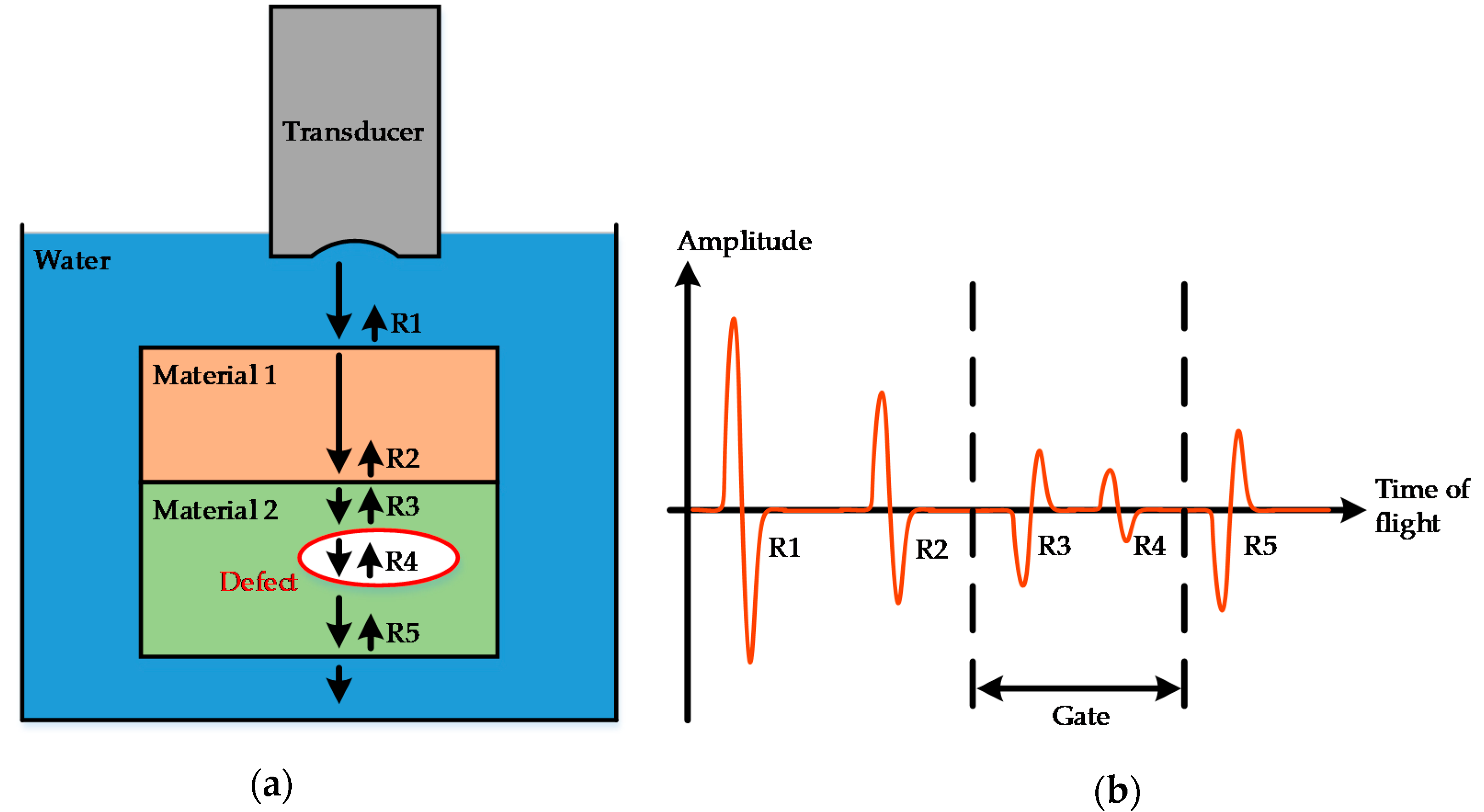
3.2. Scanning Acoustic Microscopy (SAM)

SAM uses acoustic waves in the range of 15 to 300 MHz to inspect material surfaces and volumes [29]. The centerpiece of SAM is a transducer emitting a focused acoustic wave toward the specimen placed in water as a couplant. The wave penetrates the specimen and is partially absorbed by the material, scattered at fine structures, or reflected at interfaces between two materials according to their difference in acoustic impedances depending on material density and acoustic velocity. Interfaces for acoustic waves also include defects inside a single material being an interface from material to, e.g., gas for voids/pores and the reverse [30]. Reflections caused by an interface vertical to the wave propagation direction are reflected straight back, and the transducer records the echo time resolved holding several interface reflections with different signal propagation delays (referred to as time of flight) [31,32]. A simplified set-up including a potential echo signal for a given specimen is displayed in Figure 2 with further explanations in the caption. By inspecting the pattern and time of flight inside certain time intervals of the complete echo, single layers or single interfaces can be evaluated. This process is called gating. For the given example in Figure 2, a time gate is set between R2 and R5 to inspect material 2 for defects. In the case of defects, reflections are present within the gate and no reflections are seen when no defects are present.
The result of the described measurement in Figure 2 holds material information only in one dimension, the z-direction (propagation direction of acoustic wave and echo). Information in the x and y-directions is not included due to the focusing of the wave on a small finite area. A planar analysis is possible by raster-scanning with the transducer over the specimen and afterward combining the data to a 2D image holding the 3D information of one gate.
In contrast to X-ray, SAM allows the detection of cracks and delaminations. Both are material separations causing a reflection due to the transition from material to air, including gas or vacuum, and back even if the gap is minute [7]. Furthermore, varieties in the porosity of sintered interconnects are detectable as many small interfaces. However, SAM is limited while measuring through complex material shapes, inhomogeneous layer structures and penetration depth Complex shapes of, e.g., bond/ribbon wires and woven fiberglass cloth of FR-4 materials scatter the wave in multiple directions and prohibit a back reflection to the transducer. Inhomogeneous layer structures, meaning that, in one planar layer, different materials with different acoustic velocity are used, impede the gating due to the nonuniform time of flight. The penetration depth strongly depends on the used frequency. Lower frequencies show a higher penetration depth, but limit the resolution due to poorer focusing.

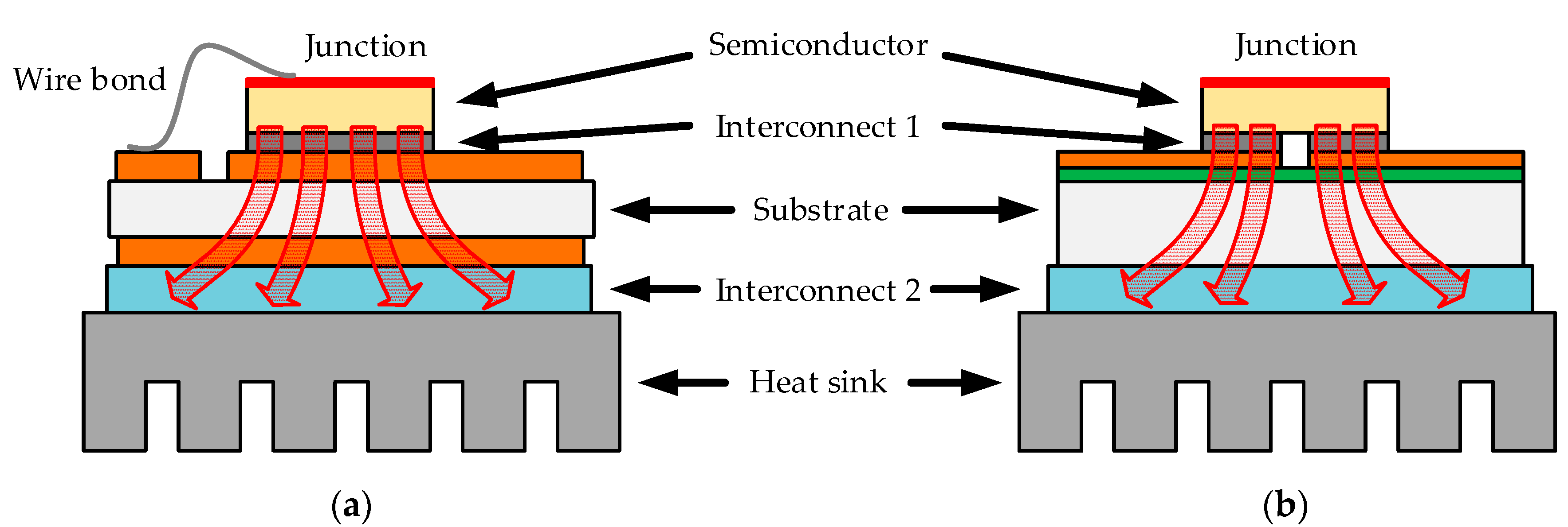
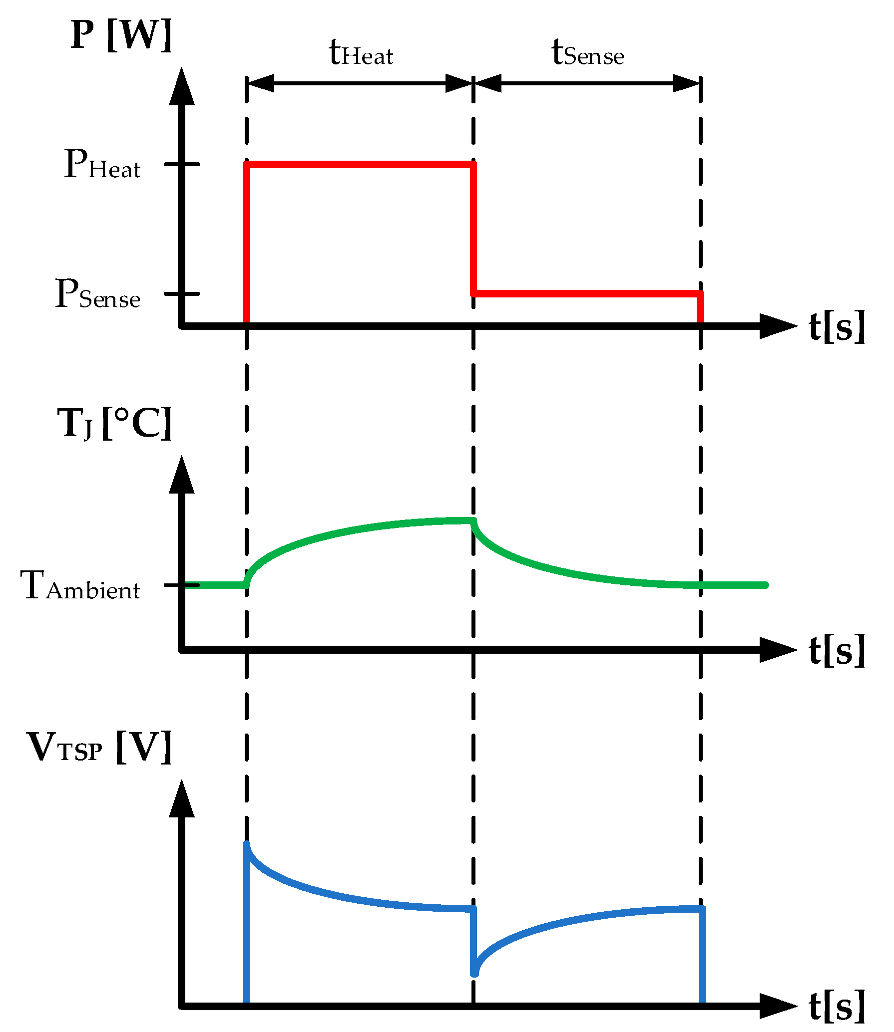
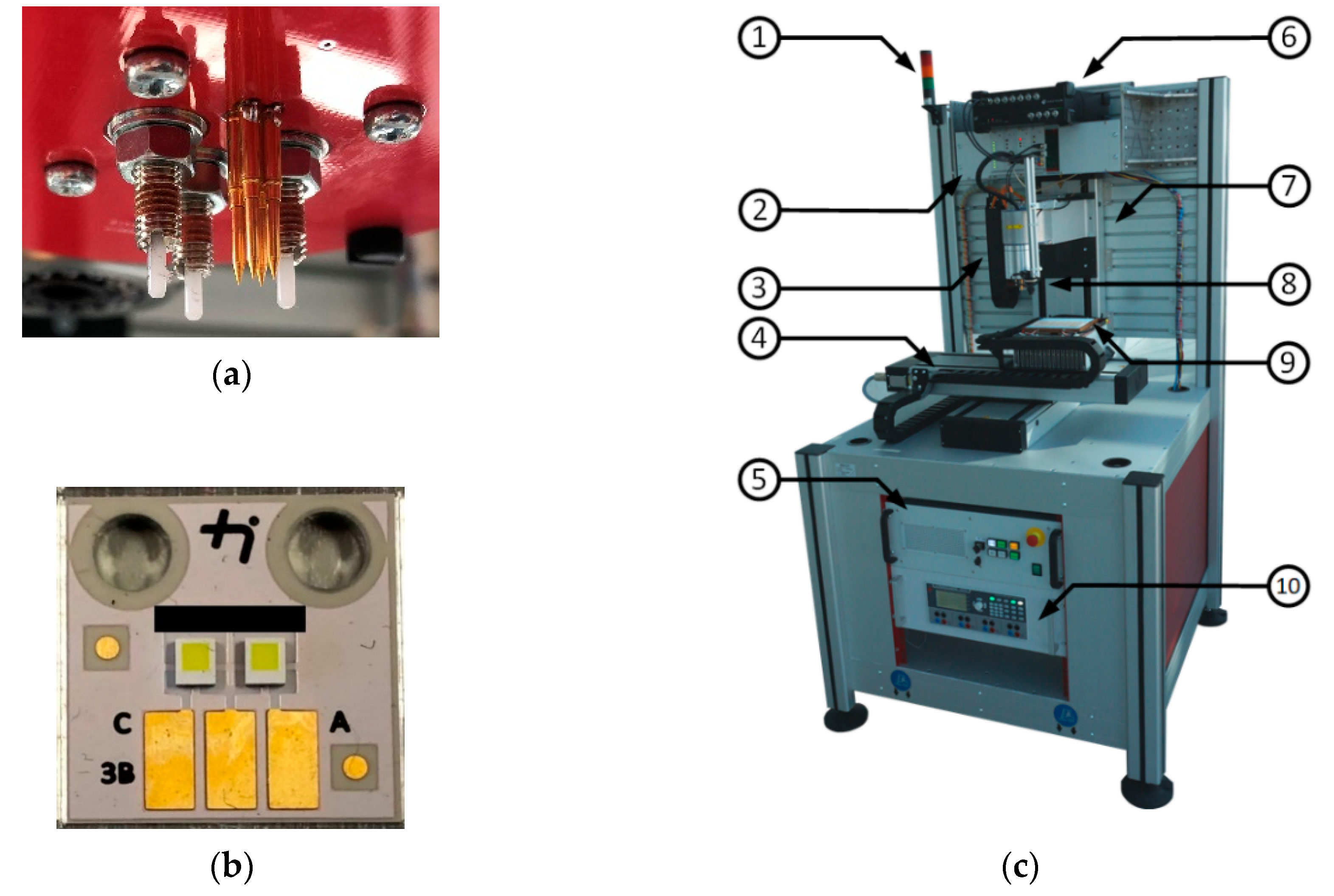
3.3. Transient Thermal Analysis (TTA)

TTA on semiconductors is an electrical test method to evaluate the thermal behavior of semiconductors in a thermomechanical set-up. The key parameter is the thermal impedance Zth(t) defining the temperature change in the semiconductor junction ΔTJ(t) according to a change in power P.
Z t h ( t ) =   Δ T J ( t ) P .
The measurement procedure of TTA for semiconductors is generally defined in [33] and refined for diodes [34], LEDs [35], MOSFETs [36], IGBTs [37,38], bipolar transistors [39], and integrated circuits (ICs) [40]. However, the measurement principle and measurement sequence are identical for all of them and the measurement sequence is visualized in Figure 3. At the beginning, an internal power loss PHeat is applied for the duration tHeat to heat up the semiconductor by driving it in some electrical operation condition. Depending on the type of semiconductor, different conditions for heating can be used, e.g., by operating diodes and LEDs in the forward direction with nominal current [41] or operating MOSFETs in the saturation region [42]. After tHeat, PHeat is switched off very quickly to a much lower power level PSense, and the semiconductor stays in this condition for the duration tSense and cools down. During tSense, the temperature of the semiconductor junction is measured and time-resolved via a temperature-sensitive electrical parameter (TSP) of the semiconductor itself. For different kinds of semiconductors, different TSPs are used, e.g., for diodes and LEDs, the forward voltage Vf [41], and, for MOSFETs, the threshold voltage Vth [42], generally called VTSP(t) in the following. ΔTJ(t) is calculated over ΔVTSP(t) and the sensitivity (SEN) of the TSP with
Δ T J ( t ) =   Δ V T S P ( t ) S E N =   V T S P ( t ) V T S P ( 0 ) S E N .
It should be mentioned that, in some standards and publications, the k-factor is used instead of SEN, which is basically its reciprocal.
Zth(t) is calculated afterward from ΔTJ(t) and the power step from PHeat to PSense with Equation (1), and it is the basis for any evaluation in TTA. The simplest evaluation method is comparing the thermal resistance Rth, being the steady-state termination value Zth(∞); however, in that way, only the performance of the whole thermomechanical set-up can be analyzed. If an evaluation of the thermal properties of different material layers inside the thermomechanical set-up is required, Zth(t) curves have to be compared on a logarithmic timescale as in Figure 4a. The three curves overlap until the point of separation where the thermal paths of the thermomechanical set-ups start to differ. Depending on the position in time of the separation, the defective material layer can be identified. An earlier separation denotes the defective layer being located closer to the heat-generating junction of the semiconductor and vice versa.
In addition to the Zth(t) comparison, there are also deeper mathematical evaluations such as the normalized logarithmic derivative. For this method, the time is substituted by z = ln(t) and, afterward, the data are derived by z and logarithmized, resulting in
B ( z ) = l o g ( 1 S E N P ) + l o g ( d V T S P ( z ) d z ) .
The advantage of this method is that VTSP(0) is eliminated by the derivation, and SEN and P are converted to a linear offset by the logarithm, which is balanced by normalization. A time-intensive determination of these parameters is no longer required. An exemplary evaluation of the data can be seen in Figure 4b with the same dataset as in Figure 4a. Equation (3) is used on all, and the normalization is performed in an interval from 100 to 1000 µs. The region of interest is the highest peak, where an increase of 0.05 can be interpreted as a failure [43,44,45].
In addition to the normalized logarithmic derivative, the structure function is a common evaluation method for TTA data. A detailed explanation would be beyond the scope of this paper and can be found in [46,47,48].
Independent of the chosen type of evaluation, the signal-to-noise ratio (SNR) is always a critical parameter for TTA [11]. A simple but time-intensive way to increase SNR is averaging over several measurement repetitions. In that way, a measurement of a single semiconductor can last from several seconds up to minutes depending on time required for the set-up to reach thermal equilibrium and the repetition count. An in-line implementation is, therefore, not feasible, and high-volume studies on a laboratory level are also not practical. Currently, commercial TTA equipment is only available in manual operation mode, including electrical contacting of the semiconductor and starting the measurement process, being time-intensive for the operator and prone to failures. For this reason, we developed an automatized thermal impedance measurement equipment (ATIM), shown in Figure 5c, controlled by a central software solution and including several subsystems. The ATIM allows successive measurement of semiconductors on the panel level and reduces the time effort for the operator to a minimum [49,50].
For measurements with the ATIM, the device under test (DUT) has to be attached to a substrate with probing pads for the electrical connection with spring probes. An exemplary substrate with two LEDs and three probing pads is depicted in Figure 5b. The anode and cathode of each LED are routed separately to probing pads, whereby the central pad is shared between the cathode of one LED and the anode of the other for this substrate. The probing head with four spring probes, shown in Figure 5a, drives down to the pads in the z-direction and allows a four-wire connection. Three additional harder springs are used to increase the clamping force of substrate to a temperature-stable plate. For an automatized measurement, one or more substrates, each holding several semiconductors, are placed on the temperature-stable plate with a TIM in between for better thermal connection, and the position and orientation are detected by a camera. The software calculates the movement of the XY-stage and rotation axis, and it successively contacts all semiconductors. The actual TTA equipment consisting of a heat/sense power source and a data acquisition unit (DAQ) performs the TTA measurement with the required settings and automatically saves the data. In that way, the effort for the operator is reduced to placement of the substrate and starting the process.

4. Results

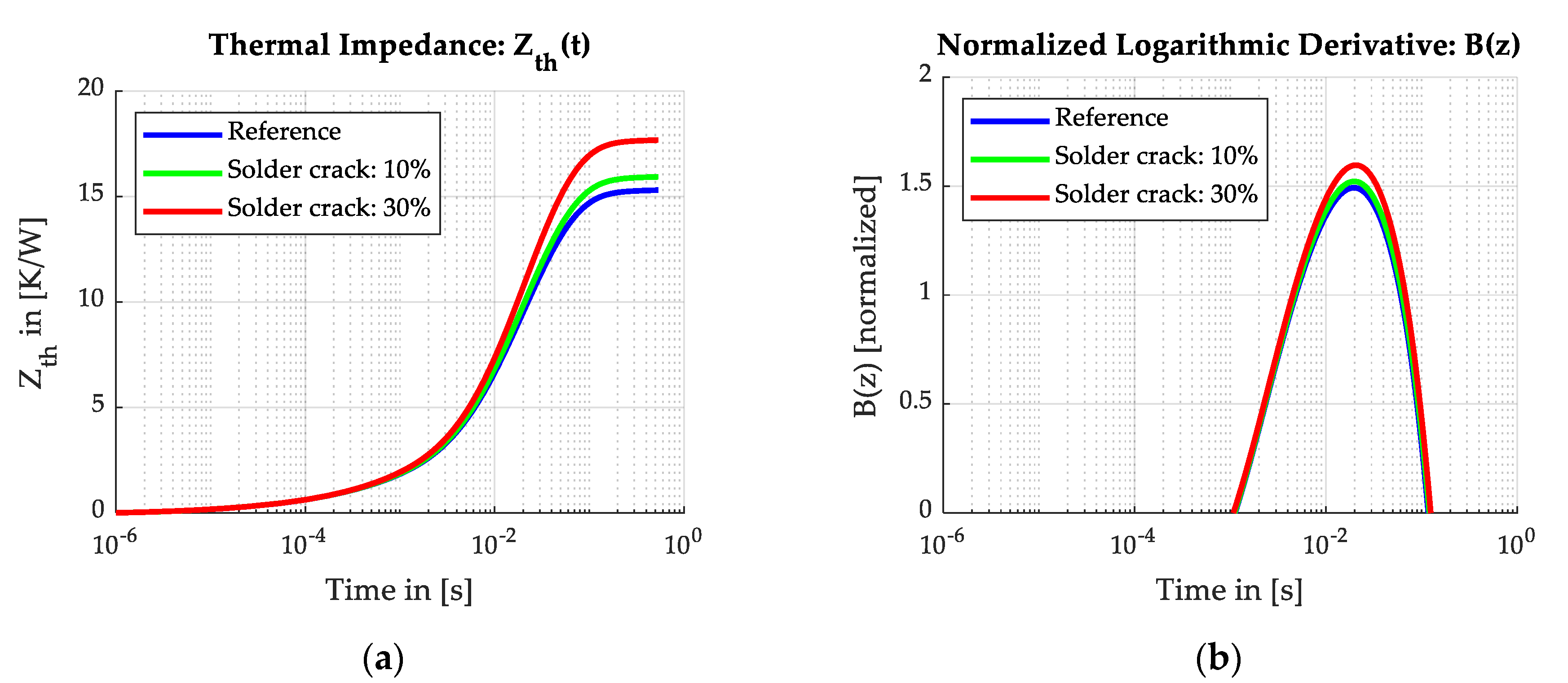
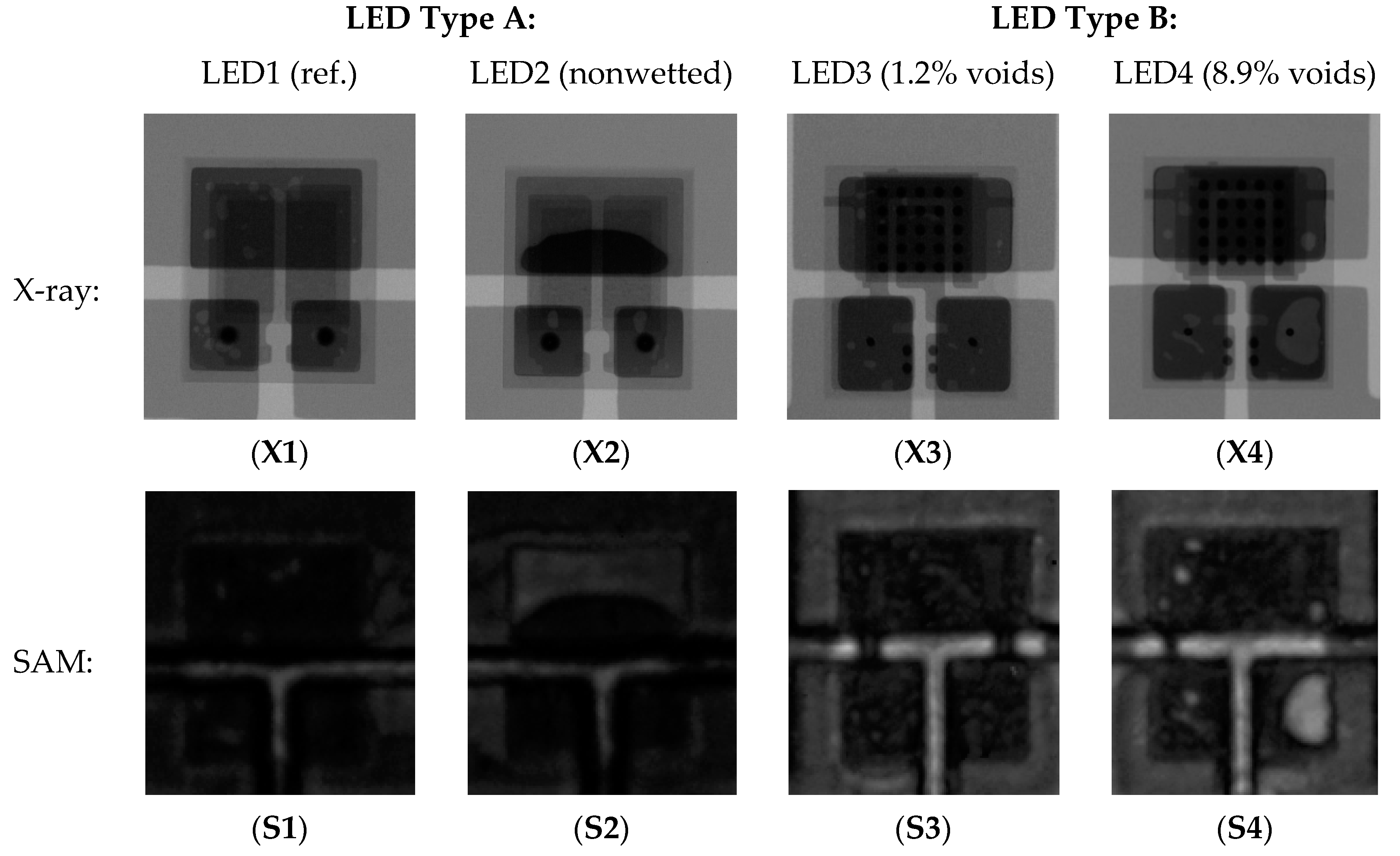
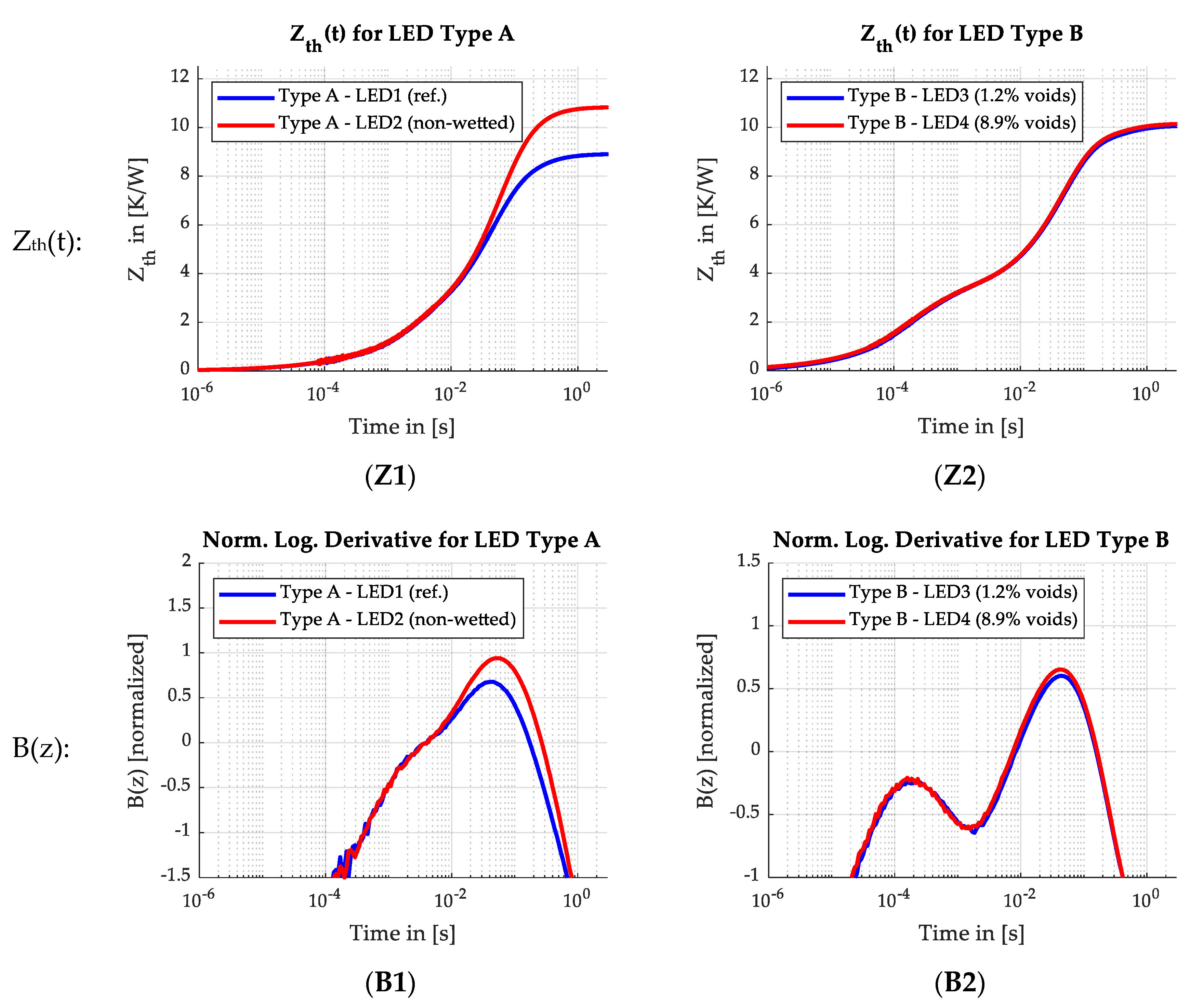
4.1. Inspection of Soldered Interface

For a comparison of the NDTs on solder interconnects, two different ceramic-based white power LEDs were analyzed with the thermomechanical set-up described in Figure 1b. An Al IMS-PCB with 70 µm copper, 50 µm dielectric material with 4.2 W/mK thermal conductivity, and 1.6 mm aluminum core was used as the substrate, and SAC105 paste was applied via stencil-printing over a 75 µm thick stencil. The package, concept, and electrical parameters of the two LED types were quite similar. Both used a ceramic carrier with three backside large-area solder pads for heat dissipation, two for electrical connection of anode and cathode, and the third as an additional insulated thermal pad. The LED dies with a surface area of approximately 1 mm2 were attached to the top side copper structure of the ceramic carrier with a planar die attach for LED type A compared with gold bumps for LED type B. On top of the die was a phosphor platelet for light conversion, and the die and phosphor were laterally optically coated with titanium oxide to prevent light emission to the sides. Both LEDs were classified for 1 A with a forward voltage Vf of about 3 V.
For SAM, the measurements were performed with a 100 MHz transducer from the backside of the substrate to investigate the solder layer. An inspection from top (LED first) was not possible, since different materials in the complex internal structures of the LED led to different propagation velocity of the acoustic wave and forbid an adequate gating to inspect specifically the solder layer. TTA measurements were run with tHeat = tSense = 3 s to reach thermal equilibrium, IHeat = 1A, and ISense = 20 mA with 10 repetitions to reduce noise. For the standard X-ray inspection, there were no noteworthy settings.
Several LEDs were inspected with the NDTs. However, a detailed discussion of the results was done only for four exemplary devices with suspicious behavior in Figure 6 including X-ray images, SAM images, and Zth(t) and B(z) plots. The figure can be vertically divided in the center with the left side belonging to LED type A and the right side to LED type B.
For LEDs of Type A, a nonwetted area was observed for one sample (LED2), and its NDT results are depicted in Figure 6 (X2) for X-ray, (S2) for SAM, (T1) for Zth(t), and (B1) for normalized logarithmic derivative. For benchmarking, the results of a good reference are additionally shown in Figure 6 (X1) and (S1) and the Zth(t) and B(z) curves added to (T1) and (B1). In (X1) of the reference, the three solder joints (top, left bottom, and right bottom) show a uniform grayish color disturbed only by voids (brighter, irregular shapes) and internal LED structures, e.g., die, copper structures, and ceramic vias (darker, orderly rectangles and circles). In (X2), this was different. The top solder joint showed an irregular-shaped dark area being darker compared to the top solder joint of (X1) and the remaining area of the top pad was brighter compared to (X1). The solder was hoarded in the darker area while the brighter area held no solder and, therefore, was nonwetted, which also resulted in a tilting of the LED by 6.5°. With SAM, the nonwetted area was also detectable in (S2) but not the hoarding, since the top pad here was not apparently different compared to the other two pads. According to the reduced soldering area, the thermal performance of the LEDs was also decreased shown in (Z1). The Zth(t) curves separated at approximately 10 ms and terminated with a difference of 1.9 K/W, being an increase of over 20% in Rth. The same was visible while comparing the normalized logarithmic derivative in (B1) with a peak increase of 0.12. A possible reason for the nonwetted area could be a contamination of the solder pad of the LED or substrate.
Analogical to LED Type A, the analysis for LED Type B was performed to evaluate the NDTs on voids in soldered interconnects. Therefore, one LED showing little voiding (LED3) and one with strong voiding (LED4) were compared in Figure 6. With X-ray in (X3) and (X4), the voids were quite visible and the void rate was calculated with 1.2% or 8.9%. Evaluation was complicated by the internal structures of the LED, particularly the ceramic vias and the gold bumps appearing as black circles. A detection of small voids behind them was not possible. With SAM in (S3) and (S4), only large voids were detectable and small ones were not detected due to the limited resolution. This effect was directly observable by comparing X-ray and SAM images. The Zth(t) analysis in (T2) revealed only minimal differences in thermal performance caused by the voids. The curves overlapped until approximately 10 ms and only slightly differed from that point. An inspection with a normalized logarithmic derivative was in this case more sensitive as shown in (B2) with a separation after the minimum turning point at 2 ms and different peaks of 0.02.
In conclusion, all NDTs were suitable for inspection of soldered interfaces. The nonwetted solder area of LED2 was detectable with all, whereby, with X-ray, the hoarding of the solder to one side of the pad was also visible unlike with SAM. With TTA, a major reduction in thermal performance was identified for LED2. Void inspection was also possible with all three NDTs, but the achieved resolution with the 100 MHz transducer for SAM was much lower compared to X-ray which also allowed the detection of small voids. A use of higher transducer frequencies was not possible for the required penetration depth. TTA revealed a slightly reduced thermal performance by voids for the two samples, but small variances in voids could not be detected by TTA. However, this revealed that they are not critical for thermal performance under a certain limit. A different aspect is the thermomechanical reliability, e.g., solder crack propagation due to temperature cycles, which can be affected by voids.

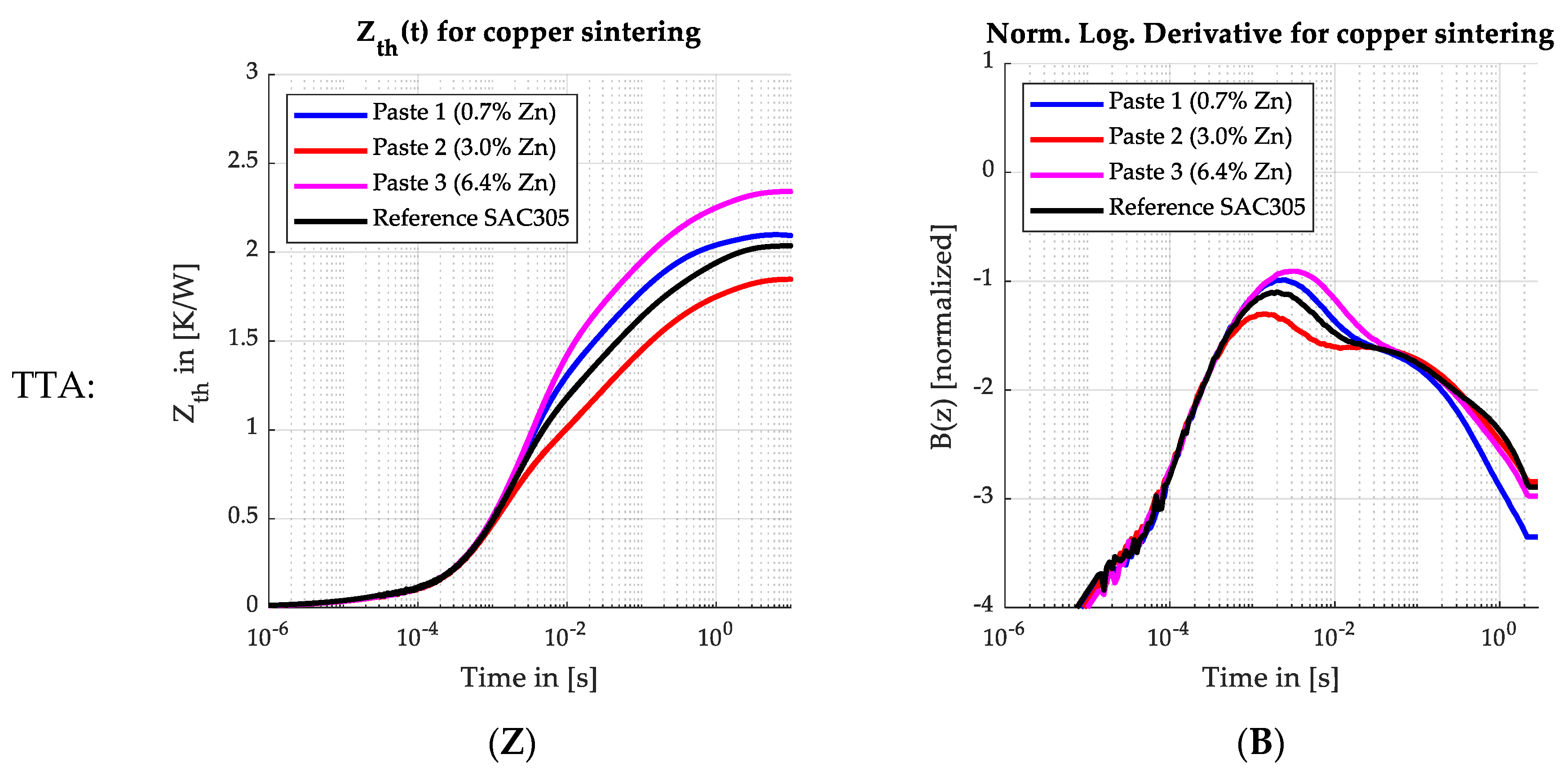
4.2. Inspection of Sintered Interfaces

The inspections of sintered interfaces were performed on bare die Si-MOSFETs with a surface of 2.3 × 2.3 mm2 and a TiNiAg backside metallization attached with an in-house developed copper sinter paste to a 1.6 mm thick copper plate with electroless nickel immersion gold (ENIG) surface finish. This thermomechanical set-up was selected to highlight the thermal characteristic of the sintered interface without any thermal low-conductive material, e.g., dielectrics overlapping. Three sinter pastes based on etched brass flakes with different percentages of remaining Zn (weight percentage: 0.7, 3.0, and 6.4) were inspected. All pastes were sintered with the same process parameters. The pastes were stencil-printed with a 75 µm stencil and predried for 5 min at 120 °C in air. Afterward, the MOSFETs were placed and sintered for 5 min under 10 MPa bonding pressure for 5 min under nitrogen atmosphere. A detailed description of pastes and process parameters can be found in [51]. A sample with SAC305 solder paste was used as reference.
The electrical connection for TTA was realized by an FR4-PCB adapter mounted on the copper sheet with a central opening for the MOSFET. Top contacts of the MOSFET were connected with Al wire bonds to the adapter PCB holding the probing pads for the ATIM. This set-up can be seen in Figure 7. TTA measurements were performed with heating in the saturation region (PHeat = 10 W) and using Vth as TSP (PSense = 0.1 W) for tHeat = tSense = 10 s with the equipment described in [42]. X-ray images and SAM images with a 100 MHz transducer were from top and were taken before wire bonding.
The results of the NDTs for the sintered interconnects are summarized in Figure 8 with X-ray inspection in (X1) to (X3) for qualification of the sintered interconnect being impossible. Even the die edges were hardly visible despite the marking of the upper right and lower left corners with red arrows. The absorption of the copper sheet overlapped the signal of the interconnect and silicon die.
In SAM images (S1) to (S3) instead, the die outline was clearly visible, and differences between the interconnects and inhomogeneities inside single interconnects were also observable. The color level correlated with the porosity of the sintered interconnect, whereby darker areas were less porous than brighter ones and bright white areas could be interpreted as local delaminations. Considering that, paste 1 was the poorest, while pastes 2 and 3 showed comparable sintering. However, an inference from SAM to the thermal performance was not possible as revealed by the TTA.
The Zth(t) curves for the three pastes and a SAC305 reference sample are plotted in (Z), and the waveforms could be separated into four time intervals referring to the four material layers. The first interval until approximately 1 ms could be assigned to the silicon of the die, and the curves overlapped within. The second interval from approximately 1 ms to 10 ms was dedicated to the sinter interface with different gradients for the pastes depending on their thermal performance. The copper plate defined the behavior in the third interval between approximately 10 ms and 100 ms, where all curves proceeded in parallel and the final interval starting afterward was assigned to the required TIM between the copper sheet and heat sink. Since the thermal performance of the TIM strongly depended on the clamping force, which was not controlled, the curves showed different trends within this interval. Therefore, only the second interval was used for evaluation, where only paste 2 showed a smaller slope meaning an improved thermal performance compared to SAC305. Pastes 1 and 3 revealed a poorer thermal performance. In the case of paste 1, delaminations as observed by SAM were a clear indication of poor thermal performance and confirmed by TTA. However, in the case of pastes 2 and 3, SAM results did not allow for a clear differentiation, while TTA was able to clearly differentiate the thermal performance of the two interconnects. By comparing the normalized logarithmic derivative in (B), the peaks could also be used to easily assess the thermal properties of the interconnects without selection of an inspection interval. A reasoning why same pastes were better than others is not part of this paper but correlated with the results from [51].
In conclusion, X-ray inspection was completely inadequate for sintered interconnects. With SAM, porosity and delaminations were detectable but a comparison of the different pastes was difficult unless in the case of clear delaminations, whereas benchmarking to standard soldered interconnects was not possible. TTA revealed the best data quality via inspection of an increase in Zth(t) within a certain time interval. In that way, the three pastes could be benchmarked to the SAC305 sample. Alternatively, the normalized logarithmic derivative was also useful for investigation by comparing the peaks without selecting a time interval.

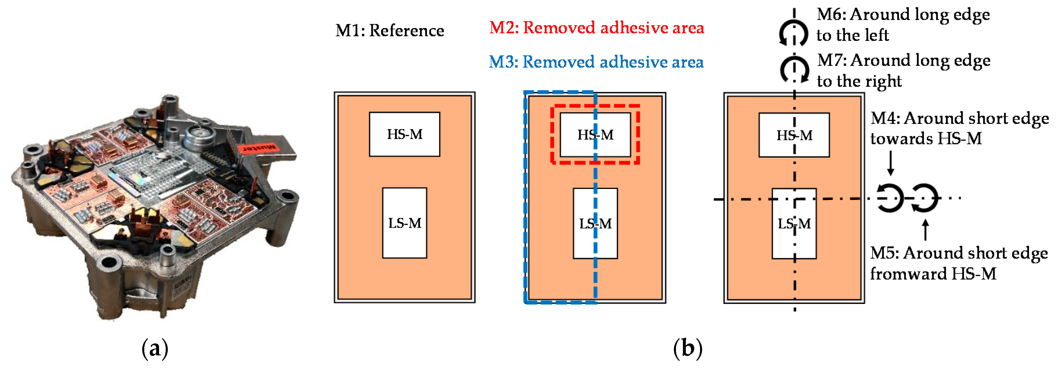
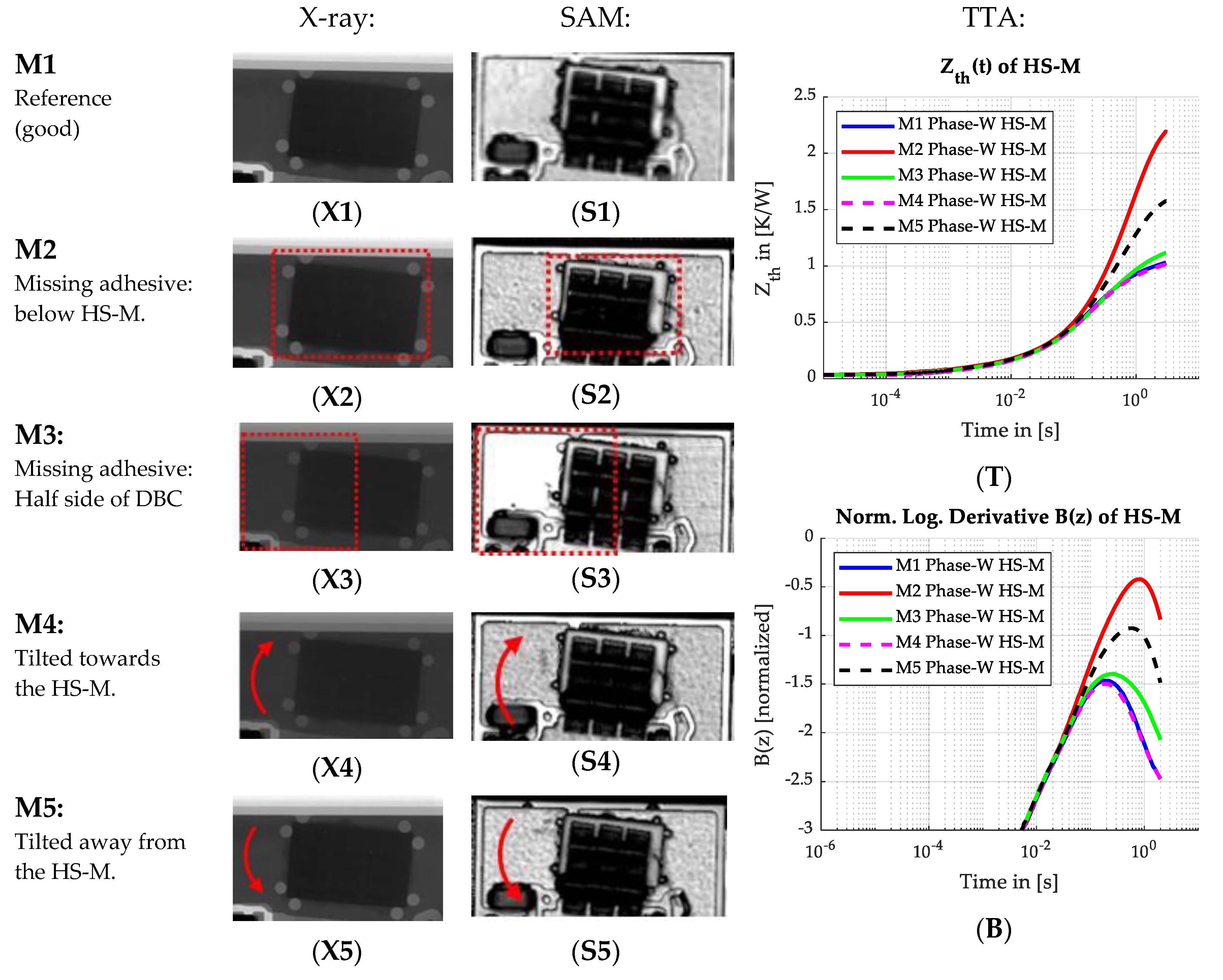
4.3. Inspection of Adhesive Interfaces

The investigations on adhesive interfaces were performed on a commercial inverter module with five half bridges depicted in Figure 9a. The thermomechanical set-up was identical to that described previously in Figure 1a. Two identical unpackaged silicon MOSFETs soldered to a DBC represented one half bridge, and each half bridge was realized on an individual DBC. Ribbon and wire bonds were used to connect the top contacts of the MOSFET dies to the DBC, and the DBCs themselves were attached with nonconductive thermal adhesive to an aluminum body used as the case and heat sink. For our investigations, the inverter modules were in a semi-fabricated state, where, amongst other things, the control unit and gate drives were missing and the connections between the half bridges and to the outer connectors were not yet present. Thus, the half bridges were isolated from each other, which allowed an individual electrical measurement required for TTA. The semi-fabricated state was reached by removing the modules at a certain point from the production line.
Overall, five modules with 50 MOSFETs were inspected. Differences in the thermal adhesive layer were evoked by manipulations within the adhesive process and, thus, the MOSFETs were divided into seven groups. Group M1 was used as a reference and was assembled without manipulation. For groups M2 and M3, the thermal adhesive was partially removed under the DBC before curing. For M2, the removal was performed below the high-side MOSFETs (HS-M) of the half bridges, and, for M3, adhesive was removed from one half of the DBC area, whereby the separation was carried out to affect the HS-M and low-side MOSFET (LS-M) in the same way. For groups M4 to M7, a tilting of the DBC was provoked by an approximately 300 µm thick wedge between the DBC and aluminum body to impede homogenic spreading of the adhesive by squeezing. These groups were separated by the direction of the tilt. M4 and M5 were tilted around the short edge of the DBC with M4 tilted toward the HS-M (no lift-off for HS-M but for the opposite side) and M5 tilted away from the HS-M (lift-off for HS-M but not for the opposite side). M6 and M7 were tilted around the long edge of the DBC with M6 tilted to the left (lift-off on the right side) and M7 tilted to the right (lift-off on the left side). All manipulations are schematically described in Figure 9b.
The results from the NDTs are summarized in Figure 10 with X-ray images, SAM images, Zth(t) curves, and normalized logarithmic derivative for one generic HS-M of groups M1 to M5. The X-ray and SAM images include markings of the area without adhesive or the tilting direction, and the Zth(t) curves are normalized to the reference module M1. Additionally, the averaged termination values of Zth(t) over all HS-Ms and LS-Ms in one group are listed in Table 1 normalized to the reference M1. SAM images were recorded with a 30 MHz transducer required to penetrate the DBC to reach the adhesive layer, but limiting the resolution and TTA performed with the same equipment from Section 4.2 with the settings PHeat = 15 W, PSense = 0.1 W, and tHeat = tSense = 3 s.
No difference between the manipulations was recognizable for X-ray inspection in (X1) to (X5) meaning that this method was inadequate to detect adhesive defects. The density of the adhesive was too small compared to the surrounding high-density metals of the aluminum body and DBC to have significant influence.
With SAM in (S1) to (S5), a failure detection in the adhesive layer was partly possible. Especially distinct was the manipulation for M3, where the removed adhesive on the left side appeared as a white area. A difference between M4 and M5 with opposite tilting directions was also detectable with a brighter section for the lifted area of M5 without a homogenic adhesive distribution. However, SAM was only useful in areas of the DBC without components or wire and ribbon bonds, disturbing the measurement by incorrect reflection angles or absorption, appearing as black shadows in the images. Therefore, for M2, no difference was detectable since the manipulated area was directly below the HS-M.
With TTA, all manipulations were detectable, including M2 having the strongest thermal degradation but not visible with SAM. All Zth(t) curves overlapped in (Z) until approximately 100 ms. Afterward, the thermal adhesive defined the behavior and the curves following different courses depending on the type of manipulation. The tilt toward the HS-M of M4, thus, showed no degradation since there was no mechanical difference compared to the reference. A tilt to the opposite direction of M5 instead had a high influence on HS-M because the lift-off was directly below. M3 showed only a slight increase affirmed by a squeezing of the thermal adhesive into the removed areas and, therefore, an increase in area and a reduction in height. A transformation of Zth(t) using the normalized logarithmic derivative showed the same results with different peak heights in (B).
Comparing the average termination values in Table 1 reveals that, with TTA, a distinction of manipulations was possible. By taking HS-M and LS-M into account, an identical trend was not observed for the two groups. It is notable that all tilting directions showed different behaviors, even for a tilt to the left or to the right. For tilting to the left (M6), the LS-M was more strongly depredated than by tilting to the right (M7). The reverse effect applied to the HS-M, where tilting to the left had a smaller influence.
In conclusion, X-ray was not applicable for adhesive investigation. The high-density material surrounding the low-density adhesive prohibited detection. With SAM, evaluation was possible only for areas without disturbing components or wire and ribbon bonds. This was problematic since the adhesive degradations directly below the MOSFETs had the highest thermal impact. An inspection with TTA seemed the most promising, whereby All defects were detected and also distinguishable.

5. Conclusions

With X-ray, SAM, and TTA, three NDTs were evaluated on the three most common interconnect technologies in the power electronics and opto-electronics industries, namely, reflow soldering, sintering, and adhesive interconnects, to prove their suitability for thermal performance and interconnect quality testing. For soldered interconnects, an X-ray inspection was sufficient to detect voids and nonwetted areas. This allowed a qualitative and fast testing with commercial X-ray equipment even at production speed for in-line measurement while manufacturing. SAM instead had a smaller resolution unable to detect small voids. TTA was able to detect nonwetted areas and revealed that void rates under a certain limit had only a minor influence on the thermal performance. However, when it came to sintered and adhesive interconnects, X-ray was unable to provide adequate data. The micro and nanopores of sintered interconnects were too small for X-ray resolution, and delaminations in the sinter interface could not be detected. In addition, the density of adhesives was too low compared to the surrounding materials of the DBC and heat sink to be visible in X-ray. With SAM, most degradation of sintered interconnects and adhesives were detectable; however, data quality strongly depended on the thermomechanical set-up. Components and wire bonds impeded the evaluation, and material thickness limited the transducer frequency and, therefore, the resolution. Moreover, the samples had to be placed in water for inspection. With TTA, all degradations of adhesive were detectable, with small differences able to be inspected even for sintered interconnects. Through the use of automatized TTA equipment, the required effort when using this method is drastically reduced and brought to a level comparable with other NDTs.

Author Contributions

Conceptualization, M.S. and G.E.; methodology, M.S. and S.K.B.; software, M.S.; validation, M.S., S.K.B., and E.L.; formal analysis, M.S.; investigation, M.S., S.K.B., E.L., and G.E.; resources, G.E.; data curation, M.S.; writing—original draft preparation, M.S.; writing—review and editing, M.S., S.K.B., E.L., and G.E.; visualization, M.S.; supervision, G.E.; project administration, G.E.; funding acquisition, G.E. All authors read and agreed to the published version of the manuscript.

Funding

The research was funded by the Bavarian Ministry of Science and Art in the project IQLED (13FH044PX8).

Acknowledgments

The authors acknowledge Andreas Riedel from Robert Bosch GmbH Ansbach for the provided materials and Gerhard Sattelberger from Hochschule Landshut for the technical support in X-ray analysis.

Conflicts of Interest

The authors declare no conflict of interest.

References

  1. Avinash, S.; Asavari, P.; Vineet, K. Power Electronics Market by Device Type (Power Discrete, Power Module, and Power IC), Material (Silicon Carbide, Gallium Nitride, Sapphire, and Other), and Application (Power Management, UPS, Renewable, and Others), and End User (Telecommunication, Industrial, Automotive, Consumer Electronics, Military & Defense, Energy & Power, and Other): Global Opportunity Analysis and Industry Forecast, 2020–2027; Allied Market Research: Portland, USA, 2020. [Google Scholar]
  2. Ruchal, H.; Vineet, K. Solid State Lighting Market by Type (Light Emitting Diodes (LED), Organic Light Emitting Diodes (OLED), and Polymer Light Emitting Diodes (PLED)), Installation Type (New Installation and Retrofit), and Application (Indoor Lighting, Outdoor Lighting, and Specialty Lighting), and Industry Vertical (Residential, Industrial and Commercial, Medical, Transportation, Others): Global Opportunity Analysis and Industry Forecast, 2020–2027; Allied Market Research: Portland, USA, 2020. [Google Scholar]
  3. Wang, H.; Liserre, M.; Blaabjerg, F. Toward Reliable Power Electronics: Challenges, Design Tools, and Opportunities. IEEE Ind. Electron. Mag. 2013, 7, 17–26. [Google Scholar] [CrossRef] [Green Version]
  4. Schulz-Harder, J. Advantages and new development of direct bonded copper substrates. Microelectron. Reliab. 2003, 43, 359–365. [Google Scholar] [CrossRef]
  5. Asai, S.; Funaki, M.; Sawa, H.; Katō, K. Fabrication of an insulated metal substrate (IMS), having an insulating layer with a high dielectric constant. IEEE Trans. Components, Hybrids, Manuf. Technol. 1993, 16, 499–504. [Google Scholar] [CrossRef]
  6. Wintrich, A.; Nicolai, U.; Tursky, W.; Reimann, T. Application Manual Power Semiconductors, 2nd ed.; ISLE Verlag: Ilmenau, Germany, 2015; ISBN 9783938843833. [Google Scholar]
  7. Aryan, P.; Sampath, S.; Sohn, H. An Overview of Non-Destructive Testing Methods for Integrated Circuit Packaging Inspection. Sensors 2018, 18, 1981. [Google Scholar] [CrossRef] [PubMed] [Green Version]
  8. Rudzki, J.; Jensen, L.; Poech, M.; Schmidt, L.; Osterwald, F. Quality Evaluation for Silver Sintering Layers in Power Electronic Modules. In Proceedings of the CIPS 2012, 7th International Conference on Integrated Power Electronics Systems, Nuremberg, Germany, 6–8 March 2012; incl. CD-ROM. VDE-Verl.: Berlin, Germany, 2012. ISBN 9783800734146. [Google Scholar]
  9. da Silva, L.F.M.; Öchsner, A.; Adams, R.D. Handbook of Adhesion Technology, 2nd ed.; Springer International Publishing: Cham, Switzerland, 2018; ISBN 978-3-319-55411-2. [Google Scholar]
  10. Elger, G.; Schmid, M.; Hanss, A. Thermal Analysis Of Semiconductor Devices. Available online: https://uspto.report/patent/app/20200018711 (accessed on 27 November 2020).
  11. Schmid, M.; Bhogaraju, S.K.; Hanss, A.; Elger, G. A new Noise-Suppression Algorithm for Transient Thermal Analysis in Semiconductors over Pulse Superposition. IEEE Trans. Instrum. Meas. 2020, 1. [Google Scholar] [CrossRef]
  12. Schmid, M.; Hanss, A.; Bhogaraju, S.K.; Elger, G. Time Saving Averaging Algorithm for Transient Thermal Analyses over Deterministic Pulse Superposition. In Proceedings of the 2019 25th International Workshop on Thermal Investigations of ICs and Systems (THERMINIC), Lecco, Italy, 25–27 September 2019; Institute of Electrical and Electronics Engineers (IEEE): Piscataway, NJ, USA, 2019; pp. 1–6. [Google Scholar]
  13. Hanss, A.; Elger, G. Residual free solder process for fluxless solder pastes. Solder. Surf. Mt. Technol. 2018, 30, 118–128. [Google Scholar] [CrossRef]
  14. IPC/JEDEC. J-STD-020E. Moisture/Reflow Sensitivity Classification for Nonhermetic Surface Mount Devices; IPC: Bannockburn, IL, USA, 2014. [Google Scholar]
  15. Liu, Y.; Leung, S.Y.; Zhao, J.; Wong, C.K.; Yuan, C.A.; Zhang, G.; Sun, F.; Luo, L. Thermal and mechanical effects of voids within flip chip soldering in LED packages. Microelectron. Reliab. 2014, 54, 2028–2033. [Google Scholar] [CrossRef]
  16. Arra, M.; Shangguan, D.; Ristolainen, E.; Lepistö, T. Effect of reflow profile on wetting and intermetallic formation between Sn/Ag/Cu solder components and printed circuit boards. Solder. Surf. Mt. Technol. 2002, 14, 18–25. [Google Scholar] [CrossRef]
  17. Vandevelde, B.; Griffoni, A.; Zanon, F.; Willems, G. Methodology for Solder-Joint Lifetime Prediction of LED-Based PCB Assemblies. IEEE Trans. Device Mater. Reliab. 2018, 18, 377–382. [Google Scholar] [CrossRef]
  18. Suganuma, K.; Jiu, J. Advanced Bonding Technology Based on Nano- and Micro-metal Pastes; Springer Science and Business Media LLC: Berlin/Heidelberg, Germany, 2017; pp. 589–626. [Google Scholar]
  19. Siow, K.S.; Lin, Y.T. Identifying the Development State of Sintered Silver (Ag) as a Bonding Material in the Microelectronic Packaging via a Patent Landscape Study. J. Electron. Packag. 2016, 138, 020804. [Google Scholar] [CrossRef] [Green Version]
  20. Bhogaraju, S.K.; Mokhtari, O.; Conti, F.; Elger, G. Die-attach bonding for high temperature applications using thermal decomposition of copper(II) formate with polyethylene glycol. Scr. Mater. 2020, 182, 74–80. [Google Scholar] [CrossRef]
  21. Siow, K.S. Are Sintered Silver Joints Ready for Use as Interconnect Material in Microelectronic Packaging? J. Electron. Mater. 2014, 43, 947–961. [Google Scholar] [CrossRef] [Green Version]
  22. Jin Yim, M.; Paik, K.W. Review of Electrically Conductive Adhesive Technologies for Electronic Packaging. Electron. Mater. Lett. 2006, 2006, 183–194. [Google Scholar]
  23. Kisiel, R.; Szczepański, Z. Die-attachment solutions for SiC power devices. Microelectron. Reliab. 2009, 49, 627–629. [Google Scholar] [CrossRef]
  24. Maurer, A. Adhesive Bonding to Replace Soldering of Power Modules. Adhes. Adhes. 2017, 14, 24–27. [Google Scholar] [CrossRef]
  25. Povolotskaya, E.; Mach, P. Failure analysis of adhesive joining in electronics. In Conference Proceedings, “New Trends in Micro/Nanotechnology”, High Tatras, Slovakia, 11–15 May 2011; 2011 34th International Spring Seminar on Electronics Technology (ISSE), Tratanska Lomnica, Slovakia, 11–15 May 2011; IEEE: Piscataway, NJ, USA, 2011; pp. 247–252. ISBN 978-1-4577-2111-3. [Google Scholar]
  26. Gilfrich, J.V.; Birks, L.S. Spectral distribution of X-ray tubes for quantitative X-ray fluorescence analysis. Anal. Chem. 1968, 40, 1077–1080. [Google Scholar] [CrossRef]
  27. Martz, H.E.; Logan, C.M.; Schneberk, D.J.; Shull, P.J. X-ray Imaging. In Fundamentals, Industrial Techniques, and Applications; Martz, H.E., Logan, C.M., Schneberk, D.J., Shull, P.J., Eds.; CRC Press: Boca Raton, FL, USA, 2016; ISBN 9781315357263. [Google Scholar]
  28. Vaga, R.; Bryant, K. Recent advances in X-ray technology. In Proceedings of the 2016 Pan Pacific Microelectronics Symposium (Pan Pacific), Big Island, HI, USA, 25–28 January 2016; IEEE: Piscataway, NJ, USA, 2016. ISBN 9780988887398. [Google Scholar]
  29. Gilmore, R.S.; Tam, K.C.; Young, J.D.; Howard, D.R.; Almond, E. Acoustic microscopy from 10 to 100 MHz for industrial applications. Philos. Trans. R. Soc. London. Ser. A Math. Phys. Sci. 1986, 320, 215–235. [Google Scholar] [CrossRef]
  30. Yazdan Mehr, M.; Bahrami, A.; Fischer, H.; Gielen, S.; Corbeij, R.; van Driel, W.D.; Zhang, G.Q. An overview of scanning acoustic microscope, a reliable method for non-destructive failure analysis of microelectronic components. In Proceedings of the 2015 16th International Conference on Thermal, Mechanical and Multi-Physics Simulation and Experiments in Microelectronics and Microsystems (EuroSimE), Budapest, Hungary, 19–22 April 2015; IEEE: Piscataway, NJ, USA, 2015; pp. 1–4, ISBN 978-1-4799-9950-7. [Google Scholar]
  31. Bertocci, F.; Grandoni, A.; Djuric-Rissner, T. Scanning Acoustic Microscopy (SAM): A Robust Method for Defect Detection during the Manufacturing Process of Ultrasound Probes for Medical Imaging. Sensors 2019, 19, 4868. [Google Scholar] [CrossRef] [Green Version]
  32. Briggs, A.; Kolosov, O.V. Acoustic Microscopy, 2nd ed.; Oxford University Press: Oxford, UK, 2010; ISBN 9780199232734. [Google Scholar]
  33. JEDEC. JESD51-14. Transient Dual Interface Test Method for the Measurement of the Thermal Resistance Junction to Case of Semiconductor Devices with Heat Flow through a Single Path; JEDEC Solid State Technology Association: Arlington, VA, USA, 2010. [Google Scholar]
  34. JEDEC. JESD282B.01. Silicon Rectifier Diodes; JEDEC Solid State Technology Association: Arlington, VA, USA, 2002. [Google Scholar]
  35. JEDEC. JESD51-51. Implementation of the Electrical Test Method for the Measurement of Real Thermal Resistance and Impedance of Light-Emitting Diodes with Exposed Cooling; JEDEC Solid State Technology Association: Arlington, VA, USA, 2012. [Google Scholar]
  36. JEDEC. JESD24-3. Thermal Impedance Measurements for Vertical Power MOSFETs (Delta Source-Drain Voltage Method); JEDEC Solid State Technology Association: Arlington, VA, USA, 1990. [Google Scholar]
  37. JEDEC. JESD24-6. Thermal Impedance Measurements for Insulated Gate Bipolar Transistors; JEDEC Solid State Technology Association: Arlington, VA, USA, 1991. [Google Scholar]
  38. JEDEC. JESD24-12. Thermal Impedance Measurement for Insulated Gate Bipolar Transistors-(Delta VCE(on) Method); JEDEC Solid State Technology Association: Arlington, VA, USA, 2004. [Google Scholar]
  39. JEDEC. JESD24-4. Thermal Impedance Measurements for Bipolar Transistors (Delta Base-Emitter Voltage Method); JEDEC Solid State Technology Association: Arlington, VA, USA, 1990. [Google Scholar]
  40. JEDEC. JESD51-1. Integrated Circuits Thermal Measurement Method-Electrical Test Method (Single Semiconductor Device); JEDEC Solid State Technology Association: Arlington, VA, USA, 1995. [Google Scholar]
  41. Daiminger, F.X.; Gruber, M.; Dendorfer, C.; Zahner, T. Experimental and theoretical considerations on the offset correction of transient cooling curves of light emitting diodes based on JESD51-14. In Proceedings of the 20th International Workshop on Thermal Investigations of ICs and Systems, London, UK, 24–26 September 2014; pp. 1–6. [Google Scholar]
  42. Schmid, M.; Gordon, E. Measurement of the Transient Thermal Impedance of MOSFETs over the Sensitivity of the Threshold Voltage. In Proceedings of the 20th European Conference on Power Electronics and Applications, Riga, Latvia, 17–21 September 2018. [Google Scholar]
  43. Hans, A.; Schmid, M.; Liu, E.; Elger, G. Transient thermal analysis as measurement method for IC package structural integrity. Chin. Phys. B 2015, 24, 068105. [Google Scholar] [CrossRef]
  44. Elger, G.; Kandaswamy, S.V.; Liu, E.; Hanss, A.; Schmid, M.; Derix, R.; Conti, F. Analysis of solder joint reliability of high power LEDs by transient thermal testing and transient finite element simulations. Microelectron. J. 2015, 46, 1230–1238. [Google Scholar] [CrossRef]
  45. Hanss, A.; Liu, E.; Schmid, M.; Elger, G. The influence of voids in solder joints on thermal performance and reliability investigated with transient thermal analysis. In Proceedings of the 2015 21st International Workshop on Thermal Investigations of ICs and Systems (THERMINIC), Paris, France, 30 September–2 October 2015; Institute of Electrical and Electronics Engineers (IEEE): Piscataway, NJ, USA, 2015; pp. 1–6. [Google Scholar]
  46. Székely, V. A new evaluation method of thermal transient measurement results. Microelectron. J. 1997, 28, 277–292. [Google Scholar] [CrossRef]
  47. Székely, V.; Van Bien, T. Fine structure of heat flow path in semiconductor devices: A measurement and identification method. Solid-State Electron. 1988, 31, 1363–1368. [Google Scholar] [CrossRef]
  48. Schweitzer, D.; Pape, H.; Chen, L. Transient Measurement of the Junction-To-Case Thermal Resistance Using Structure Functions: Chances and Limits. In Proceedings of the 2008 Twenty-fourth Annual IEEE Semionductor Thermal Measurement and Management Symposium, San Jose, CA, USA, 16–20 March 2008; pp. 191–197. [Google Scholar] [CrossRef]
  49. Elger, G.; Schmid, M.; Hanss, A.; Müller, D. Automatic Panel Level Transient Thermal Tester. In LED professional Symposium + Expo 2017; Luger Research e.U.: Bregenz, Austria, 2017. [Google Scholar]
  50. Schmid, M.; Krishna, B.S.; Elger, G. Automatic Transient Thermal Impedance Tester for Quality Inspection of Soldered and Sintered Power Electronic Devices on Panel and Tile Level. In Proceedings of the 2019 IEEE 69th Electronic Components and Technology Conference (ECTC), Institute of Electrical and Electronics Engineers (IEEE), Las Vegas, NV, USA, 28–31 May 2019; pp. 2324–2330. [Google Scholar]
  51. Bhogaraju, S.K.; Conti, F.; Kotadia, H.R.; Keim, S.; Tetzlaff, U.; Elger, G. Novel approach to copper sintering using surface enhanced brass micro flakes for microelectronics packaging. J. Alloys Compd. 2020, 844, 156043. [Google Scholar] [CrossRef]
Figure 1. Typical thermomechanical set-up for power electronics (a) and solid-state lighting (SSL) (b) in a general manner with heat flow from junction to heat sink through semiconductor, interconnect 1 (single electrical contact in (a) and multi electrical contact in (b)), substrate (direct bonded copper (DBC) in (a) and insulated metal substrate printed circuit board (IMS-PCB) in (b)) and interconnect 2 with a spreading of the heat.
Applsci 10 08516 g001
Figure 2. (a) Simplified setup of scanning acoustic microscopy (SAM). Transducer and specimen (Two different materials with a defect in material 2 are placed in water as a couplant. An acoustic wave is emitted by the transducer toward the specimen, and the potential received echo of the wave for this material stack is shown in (b). The echo consists of back reflections of the wave at any material interface arriving with different propagation delays according to their depth in the stack. In this example, the reflections are caused by the interfaces from water to material 1 (reflection R1), from material 1 to material 2 (R2), from material 2 to defect (R3), from defect to material 2 (R4), and from material 2 to water (R5), and they arrive in this order at the transducer. A time gate is set between R2 and R5, which contains all reflections of defects in material 2.
Applsci 10 08516 g002
Figure 3. Measurement sequence for transient thermal analysis (TTA) with course of power P, junction temperature TJ, and voltage of temperature-sensitive parameter VTSP.
Applsci 10 08516 g003
Figure 4. Evaluation methods in TTA: (a) Zth evaluation and (b) normalized logarithmic derivative. Data are generated by an optimized FEM model in a transient thermal simulation with a crack growth of 10% or 30% in the solder joint compared to its area described in [44]. An increase of 0.63 K/W or 2.37 K/W was observed in Zth(t) and 0.012 or 0.044 in peak increase for B(z).
Applsci 10 08516 g004
Figure 5. (a) Probing adapter with four spring probes for electrical connection and three harder springs to increase clamping force. (b) Example of a substrate with two devices under test (DUTs) and three probing pads. (c) Automatized thermal impedance measurement equipment (ATIM) with subsystems (1: signal column; 2: heat/sense power source; 3: rotation axis with integrated force sensor and probing adapter; 4: XY-stage; 5: XYZA-axis controller; 6: data acquisition (DAQ) unit; 7: Z-axis; 8: camera; 9: temperature-stable base plate; 10: power supply).
Applsci 10 08516 g005
Figure 6. Comparison of nondestructive testing methods (NDTs) for soldered interconnects on four power LEDs. (X1) to (X4) show X-ray images, (S1) to (S4) show SAM images from backside with a 100 MHz transducer (images are vertically mirrored), Z1 and Z2 show Zth(t) plots, and B1 and B2 show the normalized logarithmic derivative, whereby (X1), (X2), (S1), (S2), (Z1), and (B1) belong to two LEDs of Type A and (X3), (X4), (S3), (S4), (Z2), and (B2) belong to two LEDs of Type B. For (B1) and (B2), the normalization interval was set between 0.1 ms and 1 ms resulting in a peak increase of 0.12 or 0.02.
Applsci 10 08516 g006aApplsci 10 08516 g006b
Figure 7. Sintered bare die MOSFET on ENIG metallized copper plate with FR4 adapter PCB holding the probing pads for ATIM and Al wire bonds to the MOSFET top contacts.
Applsci 10 08516 g007
Figure 8. Comparison of NDTs on three sintered copper pastes. (X1) to (X3) show X-ray images including red arrows to mark the die outline, (S1) to (S3) show SAM images with a 100 MHz transducer, (Z) shows the Zth(t), and (B) shows the normalized logarithmic derivative plot, both including the measurement of an identical sample soldered with SAC305 paste. In (Z), increases in Zth(t) between 1 ms and 10 ms of 0.78 K/W for paste 1, 0.54 K/W for paste 2, 0.89 K/W for paste 3, and 0.68 K/W for SAC305 were measured. A normalization interval from 100 µs to 400 µs was used in (B), and peak changes of 0.112 for paste 1, −0.202 for paste 2, and 0.191 for paste 3 compared to SAC305 were measured.
Applsci 10 08516 g008aApplsci 10 08516 g008b
Figure 9. (a) Image of the inspected power inverter module in a semi-fabricated state for adhesive investigation with five half bridges on five DBCs attached with nonconductive thermal adhesive to an aluminum body. The sixth DBC holds peripheric components. (b) Schematic description of adhesive manipulations on a single DBC/half bridge used for grouping.
Applsci 10 08516 g009
Figure 10. Comparison of NDTs on adhesive interconnects. (X1) to (X5) show X-ray images of one high-side MOSFET (HS-M) of each module and (S1) to (S5) show the SAM image with a 30 MHz transducer from the same HS-M. Markings of the manipulation types are included. The Zth(t) of these HS-Ms are plotted in (T) normalized to the reference M1 and the normalized logarithmic derivative in (B), with a normalization interval between 0.1 ms and 1 ms, and measured peak increases compared to M1 of 1.04 for M2, 0.68 for M3, −0.037 for M4, and 0.54 for M5 were measured.
Applsci 10 08516 g010
Table 1. Average termination value of each group normalized to HS-M or LS-M of M1. The termination value does not represent Rth since thermal equilibrium was not reached.
Gr.Description of ManipulationSample CountHigh-Side
MOSFET
Low-Side
MOSFET
M1Reference101.001.00
M2Adhesive remove under HS-M102.111.09
M3Adhesive half removed101.081.18
M4Tilt around short edge toward HS-M61.031.36
M5Tilt around short edge from HS-M62.611.24
M6Tilt around long edge to the left side41.251.57
M7Tilt around long edge to the right side41.351.4
Publisher’s Note: MDPI stays neutral with regard to jurisdictional claims in published maps and institutional affiliations.

