Article

Effect of He Plasma Exposure on Recrystallization Behaviour and Mechanical Properties of Exposed W Surfaces—An EBSD and Nanoindentation Study

1
Australian Nuclear Science and Technology Organisation, New Illawarra Road, Lucas Heights, NSW 2234, Australia
2
School of Materials Science and Engineering, University of New South Wales, Sydney, NSW 2052, Australia
3
Research School of Physics, Australian National University, Canberra, ACT 2601, Australia
*
Author to whom correspondence should be addressed.
Metals 2023, 13(9), 1582; https://doi.org/10.3390/met13091582
Submission received: 25 July 2023 / Revised: 29 August 2023 / Accepted: 1 September 2023 / Published: 11 September 2023
(This article belongs to the Special Issue Advanced Characterization and Testing of Nuclear Materials)

Abstract

:

Highlights

(i)
EBSD, nanoindentation and AFM have been used to understand the post-plasma exposure recrystallization behaviour of W.
(ii)
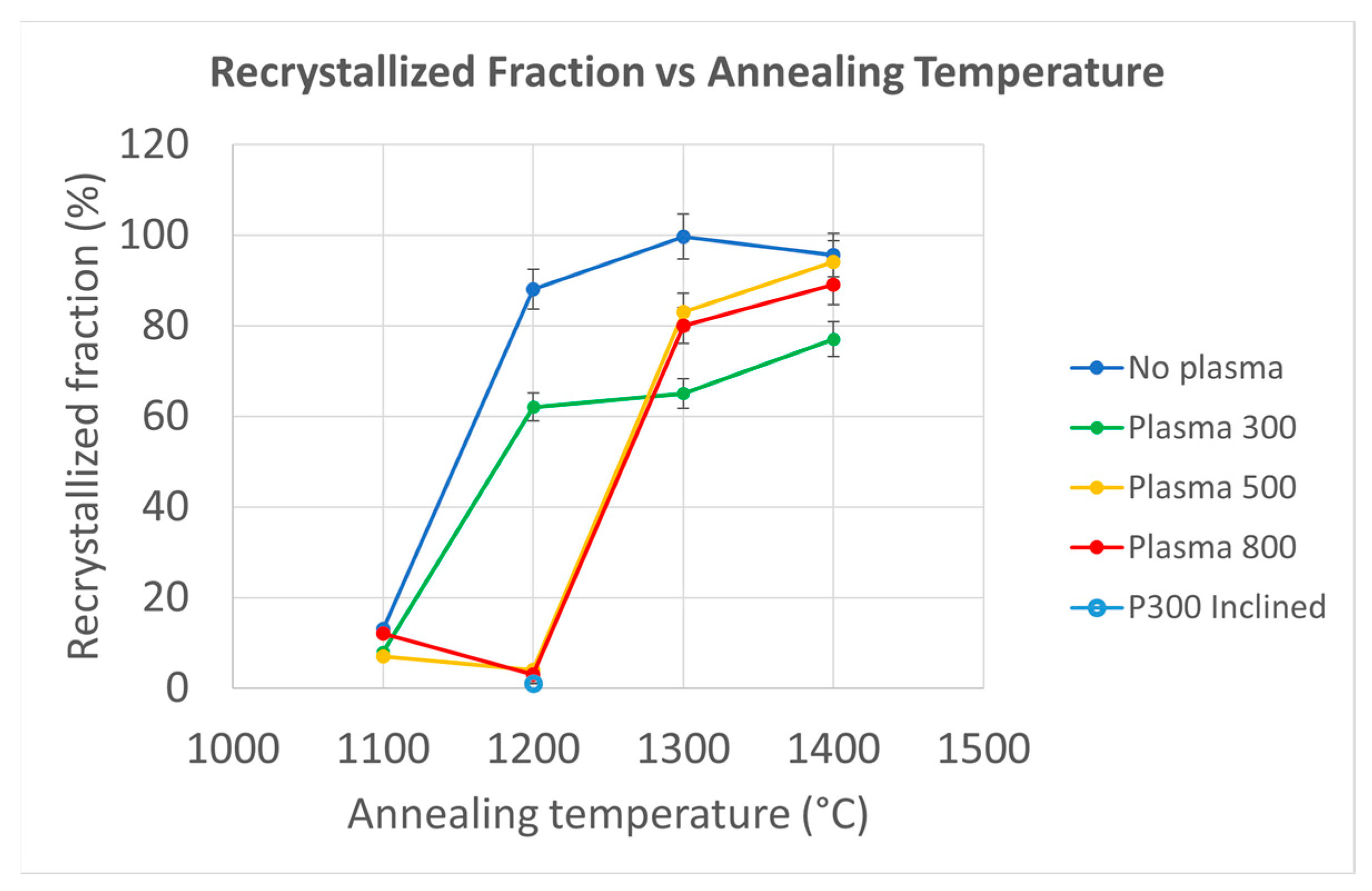
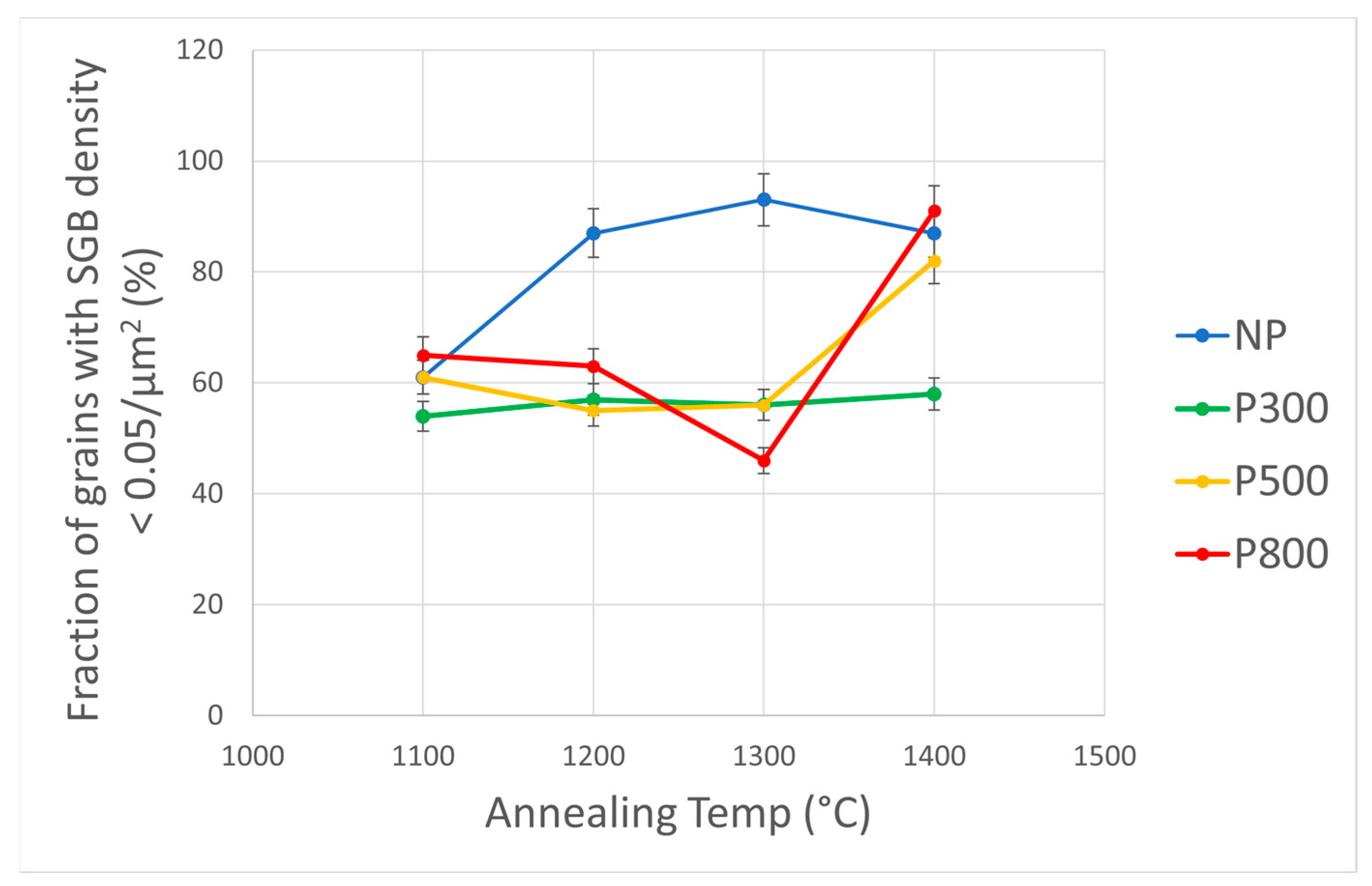
These techniques have shown that exposure to plasma at all temperatures from 300 °C to 800 °C leads to a retardation in recrystallization when annealed, especially to an annealing temperature of ~1200 °C.
(iii)
It was found the exposure to plasma at 300 °C was able to retard the recrystallization process up to an annealing temperature of 1400 °C, while higher plasma exposure temperatures (500–800 °C) were effective in slowing recrystallization only up to annealing temperatures of 1200 °C.
(iv)
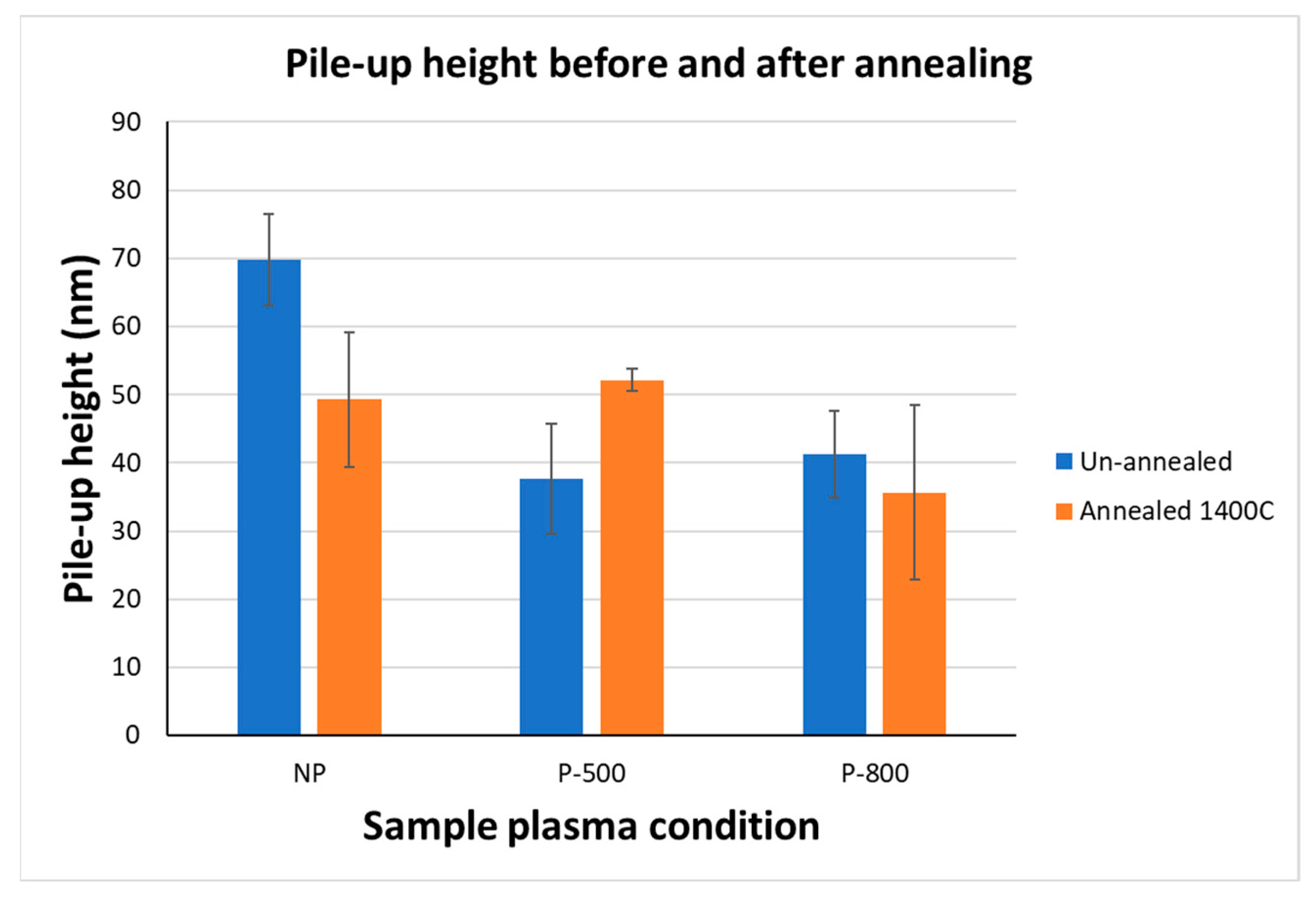
Plasma exposure and annealing did not have measurable effects on the pile-up around nanoindentation, possibly because plasma exposure itself decreases pile-up, and also retards recrystallization, which would reduce pile-up if allowed to be completed.

Abstract

Fusion reactors are designed to operate at extremely high temperatures, which causes the plasma-facing materials to be heated to 500 °C to 1000 °C. Tungsten is one of the target design materials for the plasma-facing diverter components in Tokamak designs, such as ITER, because of its excellent high-temperature strength and creep properties. However, recrystallization due to high temperatures may be detrimental to these superior mechanical properties, while exposure to He plasma has been reported to influence the recrystallization behaviour. This influence is most likely due to the Zener effect caused by He bubbles formed near the surface, which retard the migration of grain boundaries, while at the same time modifying the surface microstructure. This paper reports a study of the effect of plasma exposure at different sample temperatures on the recrystallization behaviour of W at different annealing temperatures. The characterization after plasma exposure and annealing is pursued through a series of post-exposure annealing, followed by scanning electron microscopy (SEM), electron backscatter diffraction (EBSD) characterization and nanoindentation to determine the mechanical properties. Here, it is shown that the hardness is closely related to the recrystallization fraction, and that the plasma exposure at a sample temperature of 300 °C slows down the recrystallization more than at higher sample temperatures of 500 °C and 800 °C. Atomic force microscopy (AFM) was subsequently used to determine any changes in pile-up height around the nanoindents, to probe any indication of changes in hardenability. However, these measurements failed to provide any clear evidence regarding this aspect of mechanical behaviour.

1. Introduction

Nuclear fusion is deemed to be a very attractive energy source due to a number of reasons. These include the phenomenal amount of energy released per unit mass (~four times that of fission reactions) [1], the abundance of fuel (deuterium from water, tritium from interactions with lithium during the fusion reaction), no greenhouse gas emissions, no long-term radioactive waste and the low risk of nuclear proliferation [2]. However, as is well known, there are many challenges in running a fusion reactor, as it depends on maintaining plasma at extremely high temperatures (~150,000,000 °C) [3] and confining it by the use of magnetic fields so as to avoid contact with the vacuum containment vessel [4]. The magnetic confinement of plasmas in the tokamak is a very complicated process and sophisticated techniques are being developed for their precise control, including through the use of artificial intelligence [5].
The tokamak is one of the main designs of fusion reactors and is the one selected for the International Thermonuclear Experimental Reactor (ITER) fusion reactor. The vacuum vessel containing the plasma in the ITER tokamak has the divertor located at its bottom, which channels out heat and ash from the fusion reaction and minimizes contamination by plasma while protecting the surrounding walls from thermal and neutronic loads [6]. Tungsten is the preferred candidate material for use in the plasma-facing component (armour material) of the divertor cassette in planned fusion reactors such as ITER [7,8], as it has excellent high-temperature properties such as high melting point (3422 °C), high threshold energy for sputtering (Eth~200 eV for deuterium) i.e., low erosion rate, high thermal stress resistance, high thermal conductivity, low induced activation, low swelling, and low tritium retention [9,10]. Different methods of W armour plate fabrication have been explored in recent years, including rolling [11] and plasma spray [12].
In spite of these advantages, the tungsten divertor components face some significant challenges, of which there are two major phenomena affecting the material. Firstly, tungsten exposed to He plasma is susceptible to the formation of a defect layer near the surface, consisting of tiny He bubbles [13,14,15], which can develop into a “fuzz” formed out of nanotendrils [16,17,18] with increasing dose. Secondly, W undergoes recrystallization due to the high temperatures it faces during operation. It is expected that the inner target (IT) of the divertor will reach 500 °C–1000 °C during normal operation and even up to and above 2000 °C during short-term plasma instabilities [19], which is considerably greater than the recrystallization temperature of W (~1300 °C–1400 °C through EBSD studies by Tsuchida et al. [20]). As shown by Wirtz et al. [21], recrystallization reduces the yield stress and thermal shock resistance of W and, thus, these temperature excursions can be detrimental to the life of these monoblocks after repeated thermal cycles over the lifetime. It was predicted by finite element modelling that the lifetime of tungsten monoblocks in terms of the number of 20 MW/m2, 10 s pulses and heating from 120 °C to ~2000 °C, was reduced from 884 to 52 pulses (by 94%) due to recrystallization [22].
It has been confirmed experimentally that recrystallization renders the W plasma-facing material more susceptible to cracking and thermal shock [23]. Further work on W exposed to He plasma has demonstrated that such a treatment retards recrystallization, most likely due to the formation of He bubbles, which pin the grain boundaries and thus increase the recrystallization temperature of W [24,25]. The pinning of grain boundaries by He bubbles is thought to be a manifestation of Zener drag [26,27], where the total drag force is inversely proportional to the size of the bubbles, assuming the volume fraction of bubbles is constant [24,28]. In a previous paper by the current authors, it was shown that exposure to He at sample temperatures of 300 °C, 500 °C and 800 °C for 1 h caused a suppression of recrystallization, and that this effect was the maximum in the sample exposed at 300 °C [29]. This suggests significant memory effects where prior operating conditions not only affect material properties at the time of plasma exposure but can lead to synergistic effects with future operating conditions to influence material behaviour in a non-trivial manner. This, in turn, has important implications for ITER divertor operation.
In this work, synergistic effects between He plasma exposure temperature and subsequent annealing temperature are investigated to probe the effects of higher He plasma doses and to test the reproducibility of the phenomenon. The temperatures chosen for annealing range from 1100 °C to 1400 °C, i.e., within the range of possible service temperatures, and in the vicinity of the recrystallization temperature. If He is, indeed, responsible for recrystallization suppression, it is to be expected that this increased dose would cause a stronger effect and potentially lead to greater divergence in post-annealing behaviour between different plasma exposure conditions.
This work presents a comprehensive study of the effect of high-dose He plasma exposure on the recrystallization behaviour of tungsten, through the use of multiple advanced techniques including scanning electron microscopy (SEM), electron backscatter diffraction (EBSD), nanoindentation and atomic force microscopy (AFM). All these experimental techniques, followed by detailed analysis involving recrystallized fraction, subgrain boundary density and hardness change after annealing, have been used to confirm unequivocally that plasma exposure at lower sample temperatures retards the recrystallization of W to a greater extent than exposure at higher temperatures.

2. Materials and Methods

2.1. Material and Sample Preparation

Samples were cut from a block of 99.7% pure rolled polycrystalline W manufactured by Plansee® (Plansee SE, Reutte, Austria) according to ITER specifications. The sample surfaces were kept parallel to the rolling direction. Twenty identical samples were mechanically polished and finished with 0.05 µm colloidal silica suspension at Australia’s Nuclear Science and Technology Organisation (ANSTO, Lucas Heights, Australia). A visible oxidation layer developed on the sample surface. To remove the oxide layer, a diamond film was used to polish the samples to a 1 μm finish. No stress relieving treatment of the samples was conducted.

2.2. Plasma Exposure and Annealing

Samples were split into four groups of five samples for different plasma temperatures. One group was kept un-irradiated, and the other samples were irradiated by a pulsed He ion plasma with a 50% duty cycle using Australian National University’s (ANU) MAGPIE instrument (Plasma Research Laboratory, ANU, Canberra, Australia) for 240 min at sample temperatures of 300 °C, 500 °C and 800 °C [30]. The temperatures were measured using a thermocouple at the rear of the sample holder. The base pressure of the device was 10−6 Torr. Ion implantation was carried out at a flux of 9 × 10²⁰/m2/s and ion energy of 25 eV, as determined via Langmuir probe, which is equivalent to a power density of 3.6 kW/m2 at the time the plasma is pulsed. Thus, a total flux of 6.48 × 1024/m2 was reached over a period of 4 h. Samples in each group were isochronously annealed at different temperatures of 1100 °C, 1200 °C, 1300 °C and 1400 °C, respectively, for 1 h, leaving one unannealed sample for each group. The heating and cooling of the samples were performed at rates of 2 °C/min. For details about the He plasma irradiation process, please refer to reference [29].
The analysed samples are listed below in Table 1. The convention for naming the samples is as follows—PxAy, where x is the plasma exposure temperature of the sample, and y is the annealing temperature.

2.3. Characterization

The samples were characterized using Zeiss® Ultra Plus™ SEM (Carl Zeiss Microscopy GMBH, Jena, Germany) to image surface details and microstructural features, and an Oxford Instruments ® Aztec™ detector (Oxford Instruments Nanoscience, Abingdon, Oxfordshire, UK) to acquire EBSD maps for estimating the stored deformation and recrystallization fraction.
Nanoindentation was performed to measure the hardness of the as received and annealed samples using an Agilent® nanoindenter (Agilent Technologies, Inc., Santa Clara, CA, USA), in the non-CSM (continuous stiffness method) mode. The hardness is measured as a pressure, given by dividing the load by the projected surface area. For a Berkovich tip, which is a triangular pyramid [31] with an included semi-angle of 65.03°–65.27°, this value is given by
H = P/24.5h2
where P is the load and h is the depth of the indentation [32]. This formula is modified using appropriate tip calibration to account for minor variations in the tip shape due to manufacturing differences and wear through multiple use [32]. This technique is particularly suited for hardness measurements near the surface, as required in the present case, due to its high depth resolution. The load control mode was used with two limiting loads at 5 gf and 25 gf at a loading rate of 5 nm/s. Atomic force microscopy (AFM),was performed with a Digital Instruments® (Santa Barbara, CA, USA) machine to measure the pile-up behaviour at the edges of the nanoindents.

3. Results and Discussion

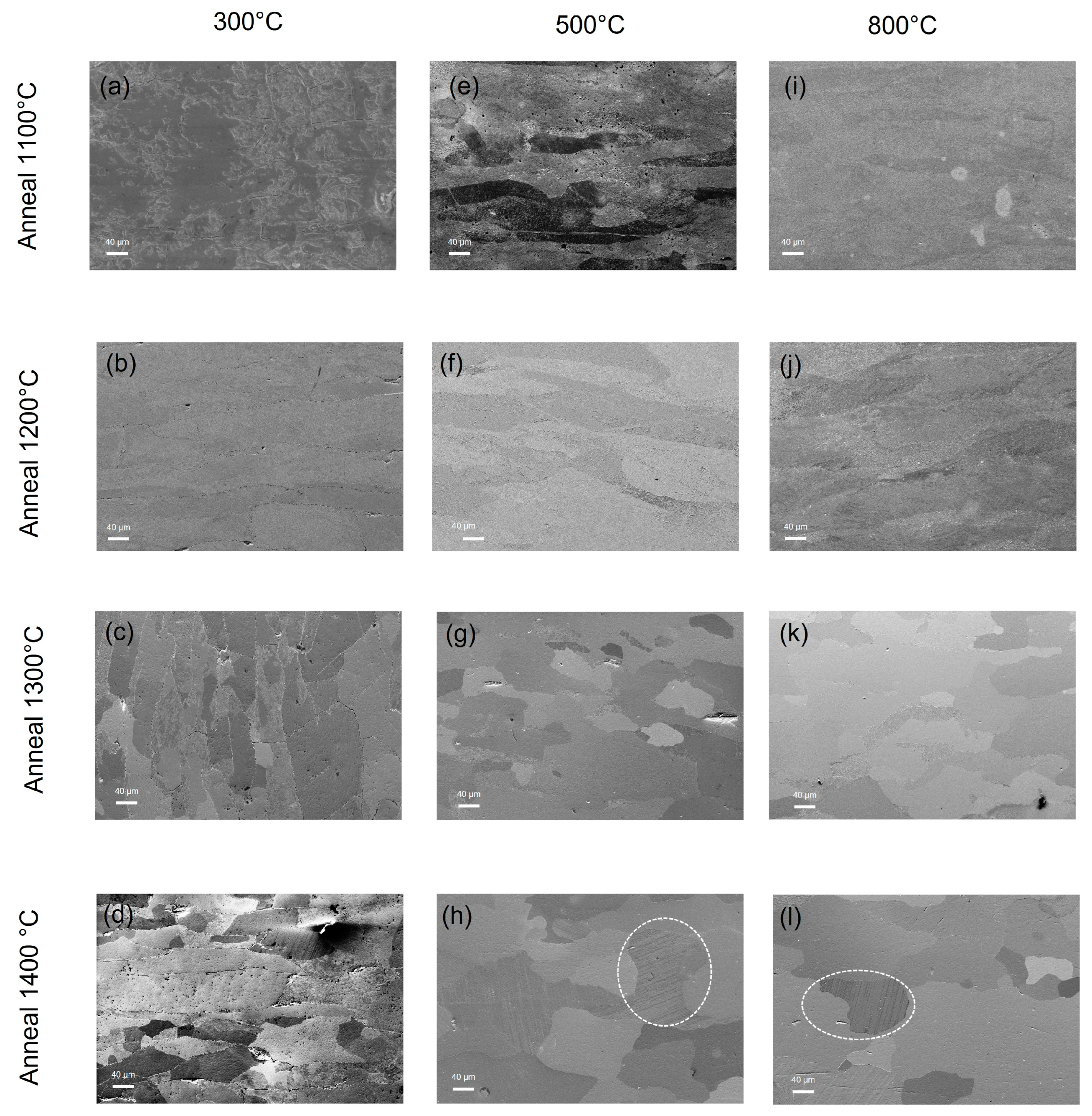
3.1. SEM Characterization

The SEM images of the as-received sample with no plasma exposure are shown in Figure 1a–e. The un-annealed sample in Figure 1a shows no clear grain boundaries but the surface exhibits some pitting, which might be caused by the removal of the oxide layer on the second polishing. Similar pitting is seen in almost all the other samples to a greater or lesser degree, with a generally decreasing trend of pitting for increasing annealing temperatures. Only the sample annealed at 1200 °C shows no pitting. The grains become more well-defined in samples annealed at temperatures ≥ 1200 °C, probably because of more recrystallization, as will be shown in the EBSD images in a latter section. The samples annealed at T ≥ 1200 °C showed large grains of the order of 50–100 µm. For samples annealed at 1300 °C and 1400 °C, grain boundary grooving was observed. This is in agreement with observations by Sachenko, et al. [33] who reported grooving at grain boundaries in W when annealed at 1350 °C. Grain boundary grooving is a well-known phenomenon that occurs during annealing in many cases due to the drive to establish equilibrium between grain boundary energy and surface tension at these locations [34]. Samples annealed at 1300 °C show some parallel surface grooves inside the grains, which become more prominent and continuous in the NP A1400 sample, as seen in the magnified image in Figure 1f. These grooves are similar to those observed by Miyamoto, et al. in their work on W exposed to He plasma [13]. There was not much grain growth visible at 1300 °C or 1400 °C compared to the grain size after 1200 °C annealing.
The SEM images of the plasma-exposed and annealed samples are shown in Figure 2. The images in Figure 2a–d show the sample exposed to plasma at 300 °C and annealed at 1100 °C, 1200 °C, 1300 °C and 1400 °C, respectively. The P300 A1100 sample showed large surface cracks up to 280 µm long and 40 µm wide, accompanied by finer cracks all along the grain boundaries. The P300 A1200 sample showed similar cracks, but there were fewer of them per unit surface area. The P300 A1300 sample showed mostly cracks at grain boundaries only, but only about 0.5 µm in width. There was also some pitting visible inside the grain. The P300 A1400 sample showed much fewer intergranular cracks and pitting, but the grain boundary cracks persisted, albeit being much thinner. The edges of the remaining big cracks were blunted after annealing at 1400 °C.
As can be seen from the SEM images in Figure 2e–h, the cracks had almost completely vanished in the samples exposed to plasma at 500 °C (P500). The surface appears somewhat rough up to an annealing temperature of 1200 °C, due to fine pitting still being present. The grains appear more prominently and are less elongated. There are some grains in Figure 2h, which show parallel grooves in the P500A1400 sample, as shown by the dashed oval.
The SEM images in Figure 2i–l show the samples exposed to plasma at 800 °C and annealed at different temperatures as above. These is still some fine pitting after annealing at 1200 °C, making the surface rough. Here, again, the cracks seem to be absent at annealing temperatures of 1200 °C and higher. Some large cracks do appear in the sample annealed at 1300 °C, but that may be due to the initial condition of the surface, where extremely large cracks might have been present. At higher annealing temperatures, the sample surfaces become smooth, with the pitting almost disappearing completely. This sample, too, has some grains which show closely placed parallel grooves in the 1400 °C annealed condition, as indicated by the dashed oval in Figure 2l. These grooves may be formed due to dislocations moving out of the surface after annealing, and are the subject of an ongoing study.
Surface cracks in the plasma-exposed samples are thought to be formed by the accumulation of He bubbles at the grain boundaries, followed by their aggregation, which causes the physical separation of grains, as reported in an earlier paper by Thompson et al. [29]. It is thought that, at low plasma exposure temperatures, the He trapped at grain boundaries (GBs) near the surface does not diffuse out and this exacerbates the agglomeration of bubbles and consequent cracking. On the contrary, at high plasma exposure temperatures, the He is able to diffuse away from the grain boundaries and so the He concentration at GBs near the surface is smaller, resulting in a weaker propensity for crack formation.
The relative smoothening of surfaces at higher temperatures is in agreement with previous observations of increasing surface healing at higher temperatures [35]. This is likely to be the result of increasing surface self-diffusion at high temperatures [36].

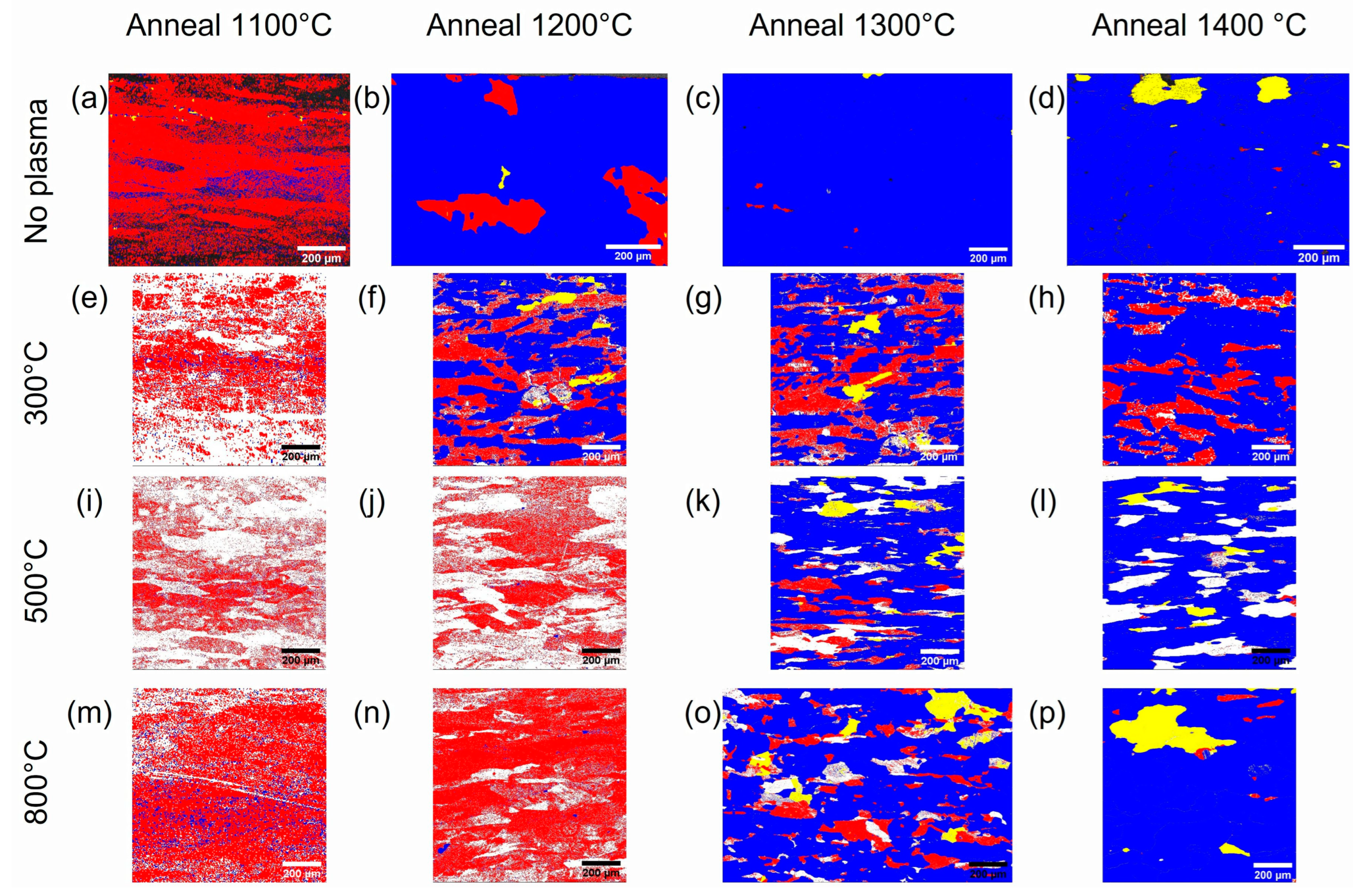
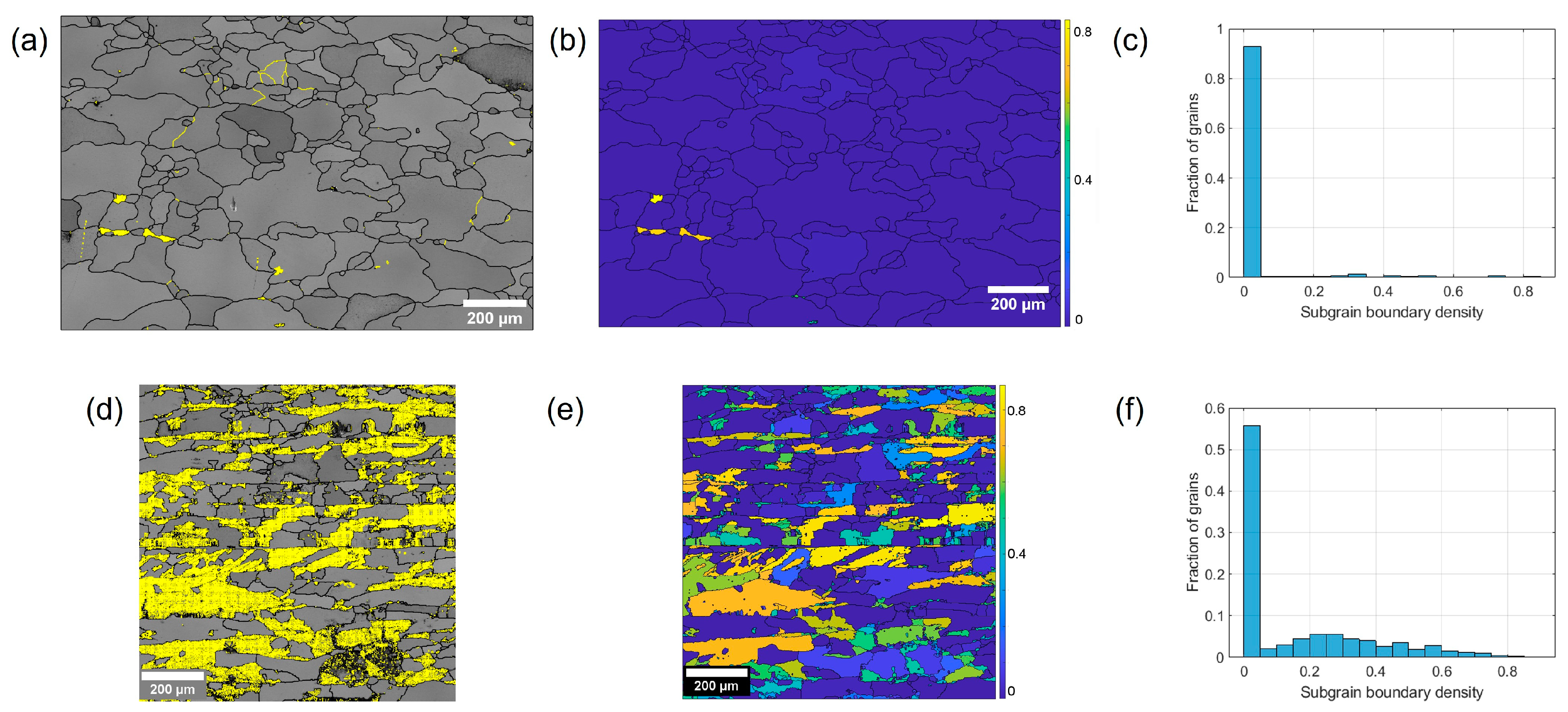
3.2. Electron Backscatter Diffraction (EBSD) Maps

The plasma-exposed and annealed samples were all scanned using the SEM to obtain EBSD data, which are presented in Figure 3 as inverse pole figure (IPF) maps. The unexposed samples are shown in Figure 3a–d, the 300 °C samples exposed to plasma (P300) in Figure 3e–h, 500 °C samples (P500) in Figure 3i–l and the 800 °C samples (P800) in Figure 3m–p. The images show, from left to right in each row, the samples after annealing at 1100°, 1200°, 1300° and 1400 °C, respectively. The as received, un-annealed sample gave very poor pattern quality, which prevented the acquisition of a reliable EBSD map. This is likely because of the stored deformation in the sample from prior rolling.
The maps in Figure 3 show, in general, an increasing fraction of indexed spots with increasing annealing temperatures for all plasma exposure temperatures, indicating recovery and recrystallization. This is also supported by the progressive replacement of elongated grains by equiaxed grains.
The “recrystallized fraction” maps in Figure 4, obtained from the same scans, show the “deformed” grains in red, “substructured” grains in yellow and the “recrystallized” grains in blue.
It can clearly be seen that the fraction of blue or recrystallized grains increases the most rapidly in the unexposed samples (no plasma) shown in the first row. The 300 °C plasma-exposed sample maintains a high area fraction of red or deformed grains even up to an annealing temperature of 1400 °C, while the 500 °C and 800 °C plasma exposed samples show a much higher fraction of recrystallized grains at annealing temperatures of 1300 °C and 1400 °C. The 300 °C plasma-exposed sample shows one anomalous behaviour at 1200 °C which shows an appreciable amount of recrystallization, while the 500 °C and 800 °C plasma-exposed samples do not show almost any recrystallization. These results are confirmed quantitatively in the plot of recrystallized fraction in Figure 5.
It is clear from this and the previous figure that, firstly, plasma exposure supresses recrystallization at all annealing temperatures, to some degree, when compared to annealing without plasma exposure. The fraction of recrystallized grains in the unexposed samples rises rapidly to ~85% after annealing at 1200 °C, and rises to 95% and greater for higher annealing temperatures, while the plasma-exposed samples annealed at 1200 °C show a much lower fraction of recrystallized grains. Secondly, it shows that there is a higher degree of recrystallization suppression for P500 and P800 samples when annealed at 1200 °C, than the P300 sample, which shows about 60% recrystallized grains. Thirdly, at higher annealing temperatures, the P300 sample shows a slightly greater degree of recrystallization suppression than the P500 and P800 samples. The latter two samples reach almost the same level of recrystallization as the unexposed sample when annealed at 1400 °C, while the suppression effect is still evident in the P300 sample. Overall, the greatest recrystallization suppression is observed at 1200 °C. In order to investigate the anomalous behaviour of the P300 A1200 sample further, a cross-section of the sample was scanned using EBSD. This was carried out in part due to the fact that the sample had already been sectioned at an inclined angle and was mounted in epoxy, which did not allow for a repeat scan on the normal surface. However, as an incidental benefit, this provided an insight into the annealing behaviour with respect to depth. The scan was performed over an area of 936 µm in the X direction and 654 µm in the Y direction. Since the sample was cut at an angle of 15° to the surface, this translates to a “true” depth of ~169 µm (654 µm × sin (15°)), which means that the lowest part of the map is at a depth of 169 µm from the irradiated surface. In Figure 6a, an IPF map of the cross section is presented, which shows elongated grains below a surface layer where the existing deformation is not conducive to good indexing. The elongated appearance is only due to the glancing angle of incline of the cross section. The recrystallized fraction image in Figure 6b shows that most of the scanned area is full of “deformed” grains wherever indexed. The plot of the recrystallized fraction in Figure 6c shows that about 3.5% grains are recrystallized and the rest (96.5%) are deformed.
When this is replotted on Figure 5 (blue open circle), it shows that even the P300 sample does not become recrystallized to any appreciable extent when annealed at 1200 °C. The “anomalous behaviour” appearing in the scan of the top surface is likely due to local texture, leading to one of two phenomena: greater He loss from the surface from certain preferred orientations [37], which can leave certain spots on the surface with low dose, resulting in faster recrystallization on annealing, or excess blistering in grains with certain orientations due to polishing differences [38], leading to surface distortion and the appearance of deformation. This line of thought is being investigated at present with further cross-sectional TEM and EBSD analysis.
The grain size was analysed for all the annealed samples for the unexposed and plasma-exposed conditions, and it was seen that, after annealing at 1100 °C, the grain size decreased to about 6–20 µm equivalent diameter in all cases. This is presumably because of the beginning of recrystallization, which causes the nucleation of a large number of small grains. Thereafter, for the unexposed samples, the grain size increased rapidly and stayed in the 50–70 µm range for the higher annealing temperatures. For the P300 samples, the grain size remained small (~10–20 µm) up to annealing temperatures of 1300 °C, indicating the slow progress of the recrystallization process, and then increased to ~39 µm at 1400 °C. For the P500 and P800 exposure conditions, the grain size remained low (~10 µm) till an annealing temperature of 1200 °C. However, annealing at higher temperatures caused grain growth of ~30 µm at 1300 °C and 55–65 µm at 1400 °C. This shows that grain growth starts sooner (i.e., at lower temperatures) for the P500 and P800 samples than in the P300 sample. This is indicative of greater retardation of recrystallization in the P300 case, in agreement with the other evidence presented here.
In order to further understand the recrystallization behaviour, the subgrain boundary density per unit area in the grains was analysed for all conditions. Subgrain boundaries (SGB) are defined here as those marking a misorientation of 1–10° in adjacent pixels. Examples of this analysis are presented in Figure 7, where the band contrast map with SGB and the SGB density map for NP A1300 sample and P300 A1300 samples are shown in (a,b) and (c,d), respectively, and the corresponding subgrain boundary density distribution (SGBD) is shown in (c) and (f), respectively.
It is seen that, in the unexposed sample annealed at 1300 °C, most grains (>90%) have a low subgrain boundary density (<0.05/µm2), while in the 300 °C plasma exposed sample, the fraction of grains with SGBD < 0.05/µm2 decreases to <60%, and there are grains with SGBD up to 0.75/µm2. Similar analysis was performed on all the annealed samples, and the data are plotted in Figure 8.
Here, it is evident that, while the no plasma (NP) sample showed a rapid increase in the fraction of grains with SGBD < 0.05/µm2 (up to 85–95% above 1200 °C annealing), the plasma-exposed samples continue to show a low fraction at these high temperatures. The 300 °C plasma-exposed sample shows a low fraction of grains (<60%) with low SGBD all the way up to 1400 °C annealing, with only a slight increase. The 500 °C and 800 °C plasma samples also maintain a low fraction of grains with low SGBD up to 1300 °C, and show a significant rise in the fraction of such grains only on annealing at 1400 °C. This analysis, therefore, constitutes further evidence that plasma exposure retards the recrystallization process in W and that exposure at 300 °C has the strongest effect in this respect.
As can be seen from Figure 4, in some of the maps, indexing is poor in some grains even after high temperature annealing, while other grains in the same area are fully indexed and recrystallized. An attempt was made to check whether there was a preferred orientation for grains which were indexed poorly, on the basis of the small fraction of points that were indexed in such grains. The EBSD map in Supplementary Figure S1a shows the major grains which have a large fraction of unindexed points, but nevertheless have a reasonable number of indexed ones, allowing the determination of grain orientation. The crystal orientations for these grains are indicated on this map using cubes. These orientations are also indicated in the pole figures shown in Supplementary Figure S1b and in the inverse pole figure in Supplementary Figure S1c. These plots indicate that none of the grains with low indexing fraction are oriented with the <100>, <110> or <111> poles parallel to the Z axis, while many are aligned with the sample Z axis parallel to directions ranging from about <112> to around <123>. A possible reason for this may be due to greater retention of He in grains oriented along these directions, causing the severe suppression of recrystallization and a reduction in indexed fraction. While this agrees somewhat with the idea of preferential He retention in grains oriented along <112> directions reported by Hammond et al. [37], they report that such effects are significant only in short time frames of <1 ns. The present results indicate that, if the indexing fractions are, indeed, governed by slow recrystallization in grains with certain orientations caused by differential He retention, then these effects may be stable for much longer durations than previously thought.
Another possible explanation for the difference in fraction of indexed points in grains with different orientations could be an orientation-dependent variation in the stored deformation or surface finish at the end of the polishing process [39], which might result in changes in the amount of blistering after plasma irradiation, as reported by Zayachuk et al. [40].
Dedicated experimental and modelling studies need to be performed to determine the precise cause and elucidate the reasons for such behaviour.

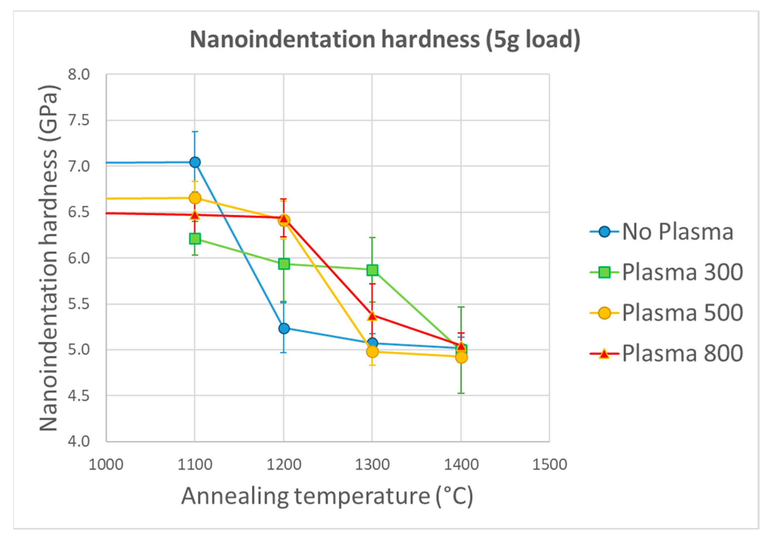
3.3. Nanoindentation

As is well known, one of the effects of annealing and resultant recrystallization is the reduction in hardness or yield strength. While there are other factors influencing the hardness, such as plasma exposure and grain orientation, the decrease in hardness in this study can be attributed entirely to the recrystallization process due to the following reasons. Firstly, the plasma exposure at the dose applied in the present case creates mostly nanoscale bubbles, which act as barriers to dislocation motion, thus increasing the strength. Secondly, while texture can affect overall strength, it is the individual orientation of grains that affect the hardness due to the anisotropy of material properties. However, the hardness of individual grains in W is not seen to depend significantly on orientation, probably due to the relatively low anisotropy of W. Both of these points are demonstrated by Zayachuk et al. in their study of W exposed to high-flux deuterium plasma [40].
As described in the experimentation section, nanoindentation was performed on the samples using a Berkovich tip on the unirradiated and plasma irradiated, un-annealed and annealed samples. The results are summarised in Figure 9. The plot in Figure 9 shows the variation in nanoindentation hardness with change in annealing temperature, as measured at a maximum load of 5 gf. The error bars denote the 95% confidence interval (CI), and are calculated as 2× standard error (SE), where SE = SD/√n, SD = standard deviation and n = no. of observations. The hardness values here are measured with a much higher load than in the previous paper, where the maximum load was 10,000 µN or ~1 gf [29]. This is the reason for the lower measured hardness in this case, since the greater load in the present case resulted in a larger indentation depth, hence a smaller indentation size effect [41]. However, the results show the same general trend as in that work, except for the fact that the drop in hardness after annealing at 1200 °C is much greater for the unexposed sample than the plasma-exposed sample in this case, in contrast to the previous work [29]. Thus, the present work demonstrates more clearly the effect of plasma exposure on retarding recrystallization than before. This difference may be due to the fact that the previous study did not include annealing at 1200 °C, which seems to be a critical temperature at which rapid recrystallization begins in the unexposed W, but which is not sufficiently high for plasma-exposed material.
It is evident from all these plots that the hardness decreases with increasing annealing temperature for all samples, as expected, due to increasing recrystallization. The “No plasma” sample shows a relatively high hardness up to an annealing temperature of 1100 °C, and then the hardness abruptly falls and stays almost constant for annealing temperatures of 1200 °C and higher. Then, the P300, P500 and P800 samples all maintain a relatively high hardness after annealing at 1200 °C, and show a statistically significant higher value compared with the NP sample. After that, the P500 and P800 samples show an abrupt decrease in hardness at 1300 °C, and this level is maintained at 1400 °C. The P300 sample also shows a decrease in hardness at 1300 °C and 1400 °C, but the overall hardness at these temperatures is slightly higher than that of the other two plasma temperatures, albeit with a statistical overlap in the 95% CI. These results are, on a first approximation, consistent with the recrystallized fraction trend. They all support the idea that plasma exposure retards recrystallization to various extents on the surface, and this suppression effect is dependent on the temperature of exposure and also of annealing. The suppression of recrystallization is most evident in the hardness measurements after annealing at 1200 °C. The softening due to recrystallization is the greatest for the P500 and P800 samples at 1300 °C annealing, and all hardness values converge at 1400 °C annealing.

3.4. Atomic Force Microscopy (AFM)

In order to assess the effect of irradiation on changes in hardenability due to annealing, the pile-up height around the nanoindents was measured using AFM. It is known that hardened metals with low hardenability show higher amounts of pile-up than annealed metals [32], so it is expected that, in general, the pile-up depth will decrease with annealing. Specifically, in tungsten samples, it was shown that annealing reduces the pile-up height in recrystallized grains by up to 50~65% [42]. The no plasma, 500 °C plasma and 800 °C plasma samples, with no annealing and 1400 °C annealing, were examined with AFM. The 300 °C samples were not studied as the surface was deemed too rough to assess the pile-up heights. The pile-up height for each edge of the indents was measured for multiple indents and averaged for each sample. A typical AFM topographical map with a profile measurement is shown in Supplementary Figure S2. The pile-up height for any given edge was measured as the height difference between the highest and lowest points on the surface along a profile line drawn perpendicular to the edge and passing through the opposing corner. The results are shown in the plot in Figure 10. It is evident from this figure that, while the pile-up has decreased measurably for the unexposed sample due to annealing, no measurable change is obvious for the 800 °C plasma samples after annealing at 1400 °C. The samples exposed to plasma at 500 °C show a slight increase in the pile-up height after annealing, which the authors cannot explain on the basis of known theory. This seems to indicate that the effect of annealing on hardenability is smaller or less significant for the plasma-exposed samples than for the unexposed samples. It has been reported by Zayachuk et al. that plasma exposure suppresses the indentation pile-up [42]. Since plasma exposure also suppresses recrystallization, which would reduce pile-up if allowed to go unhindered, plasma exposure and annealing, therefore, seem to have opposing effects on pile-up, which might be able to explain the lack of noticeable difference in pile-up in exposed samples after annealing.
Considering all the results from the EBSD recrystallization fraction, subgrain boundary density and nanoindentation, one finds incontrovertible evidence that plasma exposure suppresses or delays the recrystallization process in W on annealing, especially up to an annealing temperature of 1200 °C. The main reason behind this effect is thought to be the pinning of grain boundaries by the He bubbles, also known as the Zener effect [24]. It was shown in previous papers by some of the present authors that the retardation effect was stronger for the plasma exposure temperature of 300 °C than for higher plasma temperatures as it was thought to be causing a finer distribution of small He bubbles near the surface, which limited grain boundary migration to a greater extent [24,29]. This was suggested to be the cause as it was shown by Smith that, if the volume fraction of the second phase—in this case, the bubbles—is maintained at a constant value, the radius of curvature of the grain is proportional to the particle size [26]. Therefore, smaller bubbles will restrict the grain size to smaller values. Beyond this temperature, the 300 °C plasma exposure seems to have a slightly greater effect on recrystallization suppression than higher temperature annealing. Although the subgrain boundary density data in the present paper support this idea, the recrystallization fraction (RXF) data and the hardness data are somewhat ambiguous. While the RXF data support the idea of the stronger suppression at plasma exposure temperature of 300 °C for 1300 °C and 1400 °C annealing, it surprisingly shows consistently higher RXF at 1200 °C annealing for the P300 sample. The nanoindentation hardness data, on the other hand, shows approximately uniform suppression of the recrystallization behaviour for all plasma irradiated samples to an annealing temperature of 1200 °C and then a slightly higher suppression effect (by way of higher retained hardness) for the P300 sample at 1300 °C and 1400 °C annealing. Thus, both RXF and nano-hardness data seem to confirm the higher efficacy of 300 °C plasma exposure in recrystallization suppression at higher annealing temperatures, but the 1200 °C EBSD data seem to contradict this idea. One possible reason for this anomaly could be the texture in the EBSD scanned region of the P300A1200 sample, which might have led to rough surfaces on a larger number of grains, causing the impression of lower recrystallization. This idea is supported by the cross-sectional EBSD data of the sample shown in Figure 6. The SGB density data also support the higher efficacy of 300 °C plasma in recrystallization suppression at 1400 °C annealing, but at lower annealing temperatures, all plasma exposure temperatures seem equally effective.

4. Conclusions

Pure W samples were exposed to He plasma using the MAGPIE instrument at ANU and annealed at 1100–1400 °C at 100 °C intervals for 1 h. These samples were then characterized using SEM, EBSD, nanoindentation and AFM. The EBSD studies showed some clear trends with a few exceptions, which might be due to inhomogeneities in He retention based on the surface plane orientation of different grains.
However, in spite of that, from all the data based on EBSD and nanoindentation, the points for which there seems to be conclusive evidence are as follows:
(i)
Plasma exposure at all temperatures (300 °C, 500 °C and 800 °C) suppresses recrystallization on annealing.
(ii)
Plasma exposure at 300 °C is more effective in supressing the recrystallization on annealing, and it maintains the suppression effect even at higher annealing temperatures, while the P500 and P800 samples are more susceptible to recrystallization after 1300 °C and 1400 °C annealing.
(iii)
The hardness measured by nanoindentation agrees with these conclusions in a semi-quantitative manner.
(iv)
There is no statistically significant change in the pile-up heights after annealing, showing that the material hardenability is not affected much due to the annealing. This is possibly because plasma exposure itself decreases pile-up, and also retards recrystallization, which would reduce pile-up if allowed to be completed.
(v)
There seems to be difficulty in indexing grains which are away from any major low-indexed crystallographic axes.

Supplementary Materials

The following supporting information can be downloaded at: https://www.mdpi.com/article/10.3390/met13091582/s1, Figure S1: Orientation of grains with low indexing fraction; Figure S2: AFM scan image showing surface height around indent and measuring pile-up height.

Author Contributions

Conceptualization, D.B., M.T. and C.C.; Methodology, D.B. and M.T.; Formal analysis, D.B. and M.T.; Investigation, D.B. and C.H.; Resources, D.B. and C.C.; Writing—original draft, D.B.; Writing—review and editing, M.T., P.K. and C.C.; Supervision, D.B. All authors have read and agreed to the published version of the manuscript.

Funding

This research was partially funded by internal funding from ANSTO. This work was also partially supported by the Australian Research Council through the Discovery Project DP200102830. Additional financial support was provided by the Australian Institute of Nuclear Science and Engineering (AINSE) through an Early Career Researcher Grant.

Data Availability Statement

The data presented in this study are available on request from the corresponding author. The data are not publicly available at the moment because of further ongoing research.

Acknowledgments

The views and opinions expressed herein do not necessarily re- flect those of the ITER Organization. ITER is the nuclear facility INB 174. The authors would like to thank the NMDC division at ANSTO for allowing access to their advanced characterization and testing facilities. The authors also wish to acknowledge the valuable assistance of Tim Palmer in preparing the samples, and also Ken Short of NMDC for his help with nanoindentation and AFM experiments.

Conflicts of Interest

The authors declare no conflict of interest.

References

  1. Association, W.N. Nuclear Fusion Power. 2023. Available online: https://world-nuclear.org/information-library/current-and-future-generation/nuclear-fusion-power.aspx.2023 (accessed on 14 August 2023).
  2. ITER. Advantages of Fusion. 2023. Available online: https://www.iter.org/sci/Fusion (accessed on 14 August 2023).
  3. Jones, K.E. How Hot Is Too Hot in Fusion? 2017. Available online: https://www.olcf.ornl.gov/2017/06/27/how-hot-is-too-hot-in-fusion/ (accessed on 15 August 2023).
  4. De Tommasi, G. Plasma Magnetic Control in Tokamak Devices. J. Fusion Energy 2019, 38, 406–436. [Google Scholar] [CrossRef]
  5. Degrave, J.; Felici, F.; Buchli, J.; Neunert, M.; Tracey, B.; Carpanese, F.; Ewalds, T.; Hafner, R.; Abdolmaleki, A.; de Las Casas, D.; et al. Riedmiller, Magnetic control of tokamak plasmas through deep reinforcement learning. Nature 2022, 602, 414–419. [Google Scholar] [CrossRef] [PubMed]
  6. Walkden, N.; Riva, F.; Harrison, J.; Militello, F.; Farley, T.; Omotani, J.; Lipschultz, B. The physics of turbulence localised to the tokamak divertor volume. Commun. Phys. 2022, 5, 139. [Google Scholar] [CrossRef]
  7. ITER. Divertor. 2023. Available online: https://www.iter.org/mach/divertor (accessed on 15 August 2023).
  8. Causey, R.A.; Venhaus, T.J. The use of tungsten in fusion reactors: A review of the hydrogen retention and migration properties. Phys. Scr. 2001, 2001, 9. [Google Scholar] [CrossRef]
  9. Pintsuk, G. 4.17-Tungsten as a Plasma-Facing Material. In Comprehensive Nuclear Materials; Konings, R.J.M., Ed.; Elsevier: Oxford, UK, 2012; pp. 551–581. [Google Scholar]
  10. Webb, J.; Gollapudi, S.; Charit, I. An overview of creep in tungsten and its alloys. Int. J. Refract. Met. Hard Mater. 2019, 82, 69–80. [Google Scholar] [CrossRef]
  11. Larsen, T.; Chmelar, K.; Larsen, B.L.; Nagy, P.; Wang, K.; Pantleon, W. Thermal stability of differently rolled pure tungsten plates in the temperature range from 1125 °C to 1250 °C. Fusion Eng. Des. 2023, 192, 113581. [Google Scholar] [CrossRef]
  12. Riccardi, B.; Montanari, R.; Casadei, M.; Costanza, G.; Filacchioni, G.; Moriani, A. Optimisation and characterisation of tungsten thick coatings on copper based alloy substrates. J. Nucl. Mater. 2006, 352, 29–35. [Google Scholar] [CrossRef]
  13. Miyamoto, M.; Mikami, S.; Nagashima, H.; Iijima, N.; Nishijima, D.; Doerner, R.P.; Yoshida, N.; Watanabe, H.; Ueda, Y.; Sagara, A. Systematic investigation of the formation behavior of helium bubbles in tungsten. J. Nucl. Mater. 2015, 463, 333–336. [Google Scholar] [CrossRef]
  14. Wang, T.; Kim, H.; Wang, X.; Pacheco, A.M.; Garner, F.A.; Shao, L. Helium retention, bubble superlattice formation and surface blistering in helium-irradiated tungsten. J. Nucl. Mater. 2021, 545, 152722. [Google Scholar] [CrossRef]
  15. Nishijima, D.; Ye, M.Y.; Ohno, N. Takamura, Formation mechanism of bubbles and holes on tungsten surface with low-energy and high-flux helium plasma irradiation in NAGDIS-II. J. Nucl. Mater. 2004, 329–333, 1029–1033. [Google Scholar] [CrossRef]
  16. Baldwin, M.J.; Doerner, R.P. Helium induced nanoscopic morphology on tungsten under fusion relevant plasma conditions. Nucl. Fusion 2008, 48, 035001. [Google Scholar] [CrossRef]
  17. Kajita, S.; Yoshida, N.; Ohno, N. Tungsten fuzz: Deposition effects and influence to fusion devices. Nucl. Mater. Energy 2020, 25, 100828. [Google Scholar] [CrossRef]
  18. Takamura, S.; Ohno, N.; Nishijima, D.; Kajita, S. Formation of Nanostructured Tungsten with Arborescent Shape due to Helium Plasma Irradiation. Plasma Fusion Res. 2006, 1, 051. [Google Scholar] [CrossRef]
  19. Pitts, R.A.; Bonnin, X.; Escourbiac, F.; Frerichs, H.; Gunn, J.P.; Hirai, T.; Kukushkin, A.S.; Kaveeva, E.; Miller, M.A.; Moulton, D.; et al. Physics basis for the first ITER tungsten divertor. Nucl. Mater. Energy 2019, 20, 100696. [Google Scholar] [CrossRef]
  20. Tsuchida, K.; Miyazawa, T.; Hasegawa, A.; Nogami, S.; Fukuda, M. Recrystallization behavior of hot-rolled pure tungsten and its alloy plates during high-temperature annealing. Nucl. Mater. Energy 2018, 15, 158–163. [Google Scholar] [CrossRef]
  21. Wirtz, M.; Linke, J.; Loewenhoff, T.; Pintsuk, G. Uytdenhouwen, Thermal shock tests to qualify different tungsten grades as plasma facing material. Phys. Scr. 2016, 2016, 014015. [Google Scholar] [CrossRef]
  22. Durif, A.; Richou, M.; Kermouche, G.; Lenci, M.; Bergheau, J.M. Impact of tungsten recrystallization on ITER-like components for lifetime estimation. Fusion Eng. Des. 2019, 138, 247–253. [Google Scholar] [CrossRef]
  23. Nogami, S.; Hasegawa, A.; Fukuda, M.; Rieth, M.; Reiser, J.; Pintsuk, G. Mechanical properties of tungsten: Recent research on modified tungsten materials in Japan. J. Nucl. Mater. 2021, 543, 152506. [Google Scholar] [CrossRef]
  24. Song, K.; Thompson, M.; De Temmerman, G.; Corr, C.S. Temperature dependence of retarded recrystallisation in helium plasma-exposed tungsten. Nucl. Fusion 2019, 59, 096031. [Google Scholar] [CrossRef]
  25. Guo, W.; Cheng, L.; Temmerman, G.D.; Yuan, Y.; Lu, G.-H. Retarded recrystallization of helium-exposed tungsten. Nucl. Fusion 2018, 58, 8. [Google Scholar] [CrossRef]
  26. Smith, C.S. Grains, phases, and interfaces: An introduction of microstructure. Trans. Metall. Soc. AIME 1948, 175, 15–51. [Google Scholar]
  27. Zhu, Q.; Shao, J.; Wang, P. The Interaction between He Bubble and Migrating Grain Boundary Induced by Shear Loading. Metals 2022, 12, 12. [Google Scholar] [CrossRef]
  28. Graux, A. Microstructure Evolutions during Hot Rolling of Low Carbon Microalloyed Steels, Matériaux de Lyon; Université de Lyon: Lyon, France, 2019; p. 152. [Google Scholar]
  29. Thompson, M.A.T.; Song, K.; De Temmerman, G.; Chen, H.; Kirby, N.; Bradby, J.; Bhattacharyya, D.; Hoang, C.; Corr, C.S. Identifying microstructural changes responsible for retarded grain growth during tungsten recrystallization after helium plasma exposure. J. Nucl. Mater. 2022, 559, 153448. [Google Scholar] [CrossRef]
  30. BBlackwell, D.; Caneses, J.F.; Samuell, C.M.; Wach, J.; Corr, J.H.C. Design and characterization of the Magnetized Plasma Interaction Experiment (MAGPIE): A new source for plasma–material interaction studies. Plasma Sources Sci. Technol. 2012, 21, 055033. [Google Scholar] [CrossRef]
  31. Berkovich, E.S. Three-Faceted Diamond Pyramid for Micro-hardness Testing. Zavod. Lab. 1950, 16, 345–347. [Google Scholar]
  32. Cripps, A.C.F. Nanoindentation; Springer: New York, NY, USA, 2004. [Google Scholar]
  33. Sachenko, P.; Schneibel, J.H.; Swadener, J.G.; Zhang, W. Experimental and simulated grain boundary groove profiles in tungsten. Philos. Mag. Lett. 2000, 80, 627–631. [Google Scholar] [CrossRef]
  34. Mullins, W.W. Theory of Thermal Grooving. J. Appl. Phys. 2004, 28, 333–339. [Google Scholar] [CrossRef]
  35. Feng, C.; Wu, L.; Chen, P.; Yang, T.; Yu, B.; Qian, L. Repairing slight damages on monocrystalline silicon surface by thermal annealing. Mater. Res. Express 2021, 8, 045005. [Google Scholar] [CrossRef]
  36. Acosta-Alba, P.E.; Kononchuk, O.; Gourdel, C.; Claverie, A. Surface self-diffusion of silicon during high temperature annealing. J. Appl. Phys. 2014, 115, 134903. [Google Scholar] [CrossRef]
  37. Hammond, K.D.; Blondel, S.; Hu, L.; Maroudas, D.; Wirth, B.D. Large-scale atomistic simulations of low-energy helium implantation into tungsten single crystals. Acta Mater. 2018, 144, 561–578. [Google Scholar] [CrossRef]
  38. Shu, W.M.; Kawasuso, A.; Miwa, Y.; Wakai, E.; Luo, G.-N.; Yamanishi, T. Microstructure dependence of deuterium retention and blistering in the near-surface region of tungsten exposed to high flux deuterium plasmas of 38 eV at 315 K. Phys. Scr. 2007, 2007, 96–99. [Google Scholar] [CrossRef]
  39. Uytdenhouwen, I.; Vandermeulen, W.; Zayachuk, Y.; Kemps, R. Grain-Orientation Related Surface Effects on Polycrystalline Tungsten Caused by Mechanical Polishing and Etching. J. Mater. Sci. Eng. B 2016, 6, 161–168. [Google Scholar] [CrossRef]
  40. Zayachuk, Y.; Tanyeli, I.; Van Boxel, S.; Bystrov, K.; Morgan, T.W.; Roberts, S.G. Combined effects of crystallography, heat treatment and surface polishing on blistering in tungsten exposed to high-flux deuterium plasma. Nucl. Fusion 2016, 56, 086007. [Google Scholar] [CrossRef]
  41. Nix, W.D.; Gao, H. Indentation size effects in crystalline materials: A law for strain gradient plasticity. J. Mech. Phys. Solids 1998, 46, 411–425. [Google Scholar] [CrossRef]
  42. Zayachuk, Y.; Armstrong, D.E.J.; Bystrov, K.; Van Boxel, S.; Morgan, T.; Roberts, S.G. Nanoindentation study of the combined effects of crystallography, heat treatment and exposure to high-flux deuterium plasma in tungsten. J. Nucl. Mater. 2017, 486, 183–190. [Google Scholar] [CrossRef]
Figure 1. SEM secondary electron images of as received samples with no plasma exposure: (a) Un-annealed, (b) annealed at 1100 °C, (c) annealed at 1200 °C, (d) annealed at 1300 °C and (e) annealed at 1400 °C; (f) higher magnification image of sample annealed at 1400 °C, showing surface grooves.
Metals 13 01582 g001
Figure 2. SEM images of plasma-exposed samples (ad) 300 °C, (eh) 500 °C and (il) 800 °C, annealed at 1100 °C (a,e,i), at 1200 °C (b,f,j), at 1300 °C (c,g,k) and at 1400 °C (d,h,l). The dashed circles in (h,l) indicate grains with parallel grooves on the surface (further explanation in the text).
Metals 13 01582 g002
Figure 3. EBSD orientation maps with inverse pole figure colours for the samples (ad) unexposed, and exposed to plasma at (eh) 300 °C, (il) 500 °C and (mp) 800 °C, and annealed at 1100 °C (a,e,i,m), 1200 °C (b,f,j,n), 1300 °C (c,g,k,o) and 1400 °C (d,h,l,p).
Metals 13 01582 g003
Figure 4. Recrystallized fraction of grains as determined by Channel 5® Tango™ software (V 5.12.62.0, Oxford Instruments Nanotechnology Tools Ltd., Abingdon, Oxfordshire, UK) using 10° for grain boundary and 1° for sub-grain boundary critical angle: Red = deformed, Yellow = substructured, Blue = recrystallized. Samples with no plasma exposure—(ad), exposed to plasma at 300 °C—(eh), exposed at 500 °C—(il), and exposed at 800 °C—(m–p).
Metals 13 01582 g004
Figure 5. Recrystallized fraction at different annealing temperatures for various plasma exposure temperatures.
Metals 13 01582 g005
Figure 6. (a) IPF Z map of P300 A1200 inclined cross section sample, (b) recrystallized fraction map of the same area: red—deformed—red, recrystallized—blue, substructured—yellow, and (c) plot of the recrystallized fraction showing only about 3.5% recrystallized grains and 96.5% “deformed” grains.
Metals 13 01582 g006
Figure 7. Subgrain boundary map (black—grain boundary, yellow—subgrain boundary), subgrain boundary density (no./µm2) for each grain and corresponding normalised distribution plot for (ac) No plasma exposure, annealed at 1300 °C and (df) plasma exposure at 300 °C, annealed at 1300 °C.
Metals 13 01582 g007
Figure 8. Fraction of grains with subgrain boundary density < 0.05/µm2 at different annealing temperatures for various plasma exposure temperatures.
Metals 13 01582 g008
Figure 9. Nanoindentation hardness for various plasma exposure temperatures at different annealing temperatures.
Metals 13 01582 g009
Figure 10. Pile-up heights for unexposed, plasma exposed at 500 °C and plasma exposed at 800 °C, before and after annealing.
Metals 13 01582 g010
Table 1. List of W samples plasma irradiated at different sample temperatures and subsequently annealed at different annealing temperatures.
Sample NamePlasma Time/minPlasma Temperature/°CAnnealing Temperature/°CRef. Name
W016120300-P300ANil
W0171203001100P300A1100
W0201203001200P300A1200
W0181203001300P300A1300
W0191203001400P300A1400
W021120500-P500ANil
W0221205001100P500A1100
W0251205001200P500A1200
W0231205001300P500A1300
W0241205001400P500A1400
W026120800-P800ANil
W0271208001100P800A1100
W0301208001200P800A1200
W0281208001300P800A1300
W0291208001400P800A1400
Reference Samples
W046---PNilANil
W047--1100PNilA1100
W048--1200PNilA1200
W049--1300PNilA1300
W050--1400PNilA1400
Disclaimer/Publisher’s Note: The statements, opinions and data contained in all publications are solely those of the individual author(s) and contributor(s) and not of MDPI and/or the editor(s). MDPI and/or the editor(s) disclaim responsibility for any injury to people or property resulting from any ideas, methods, instructions or products referred to in the content.

