
Thermal Influence on Chirality-Driven Dynamics and Pinning of Transverse Domain Walls in Z-Junction Magnetic Nanowires


Abstract
1. Introduction
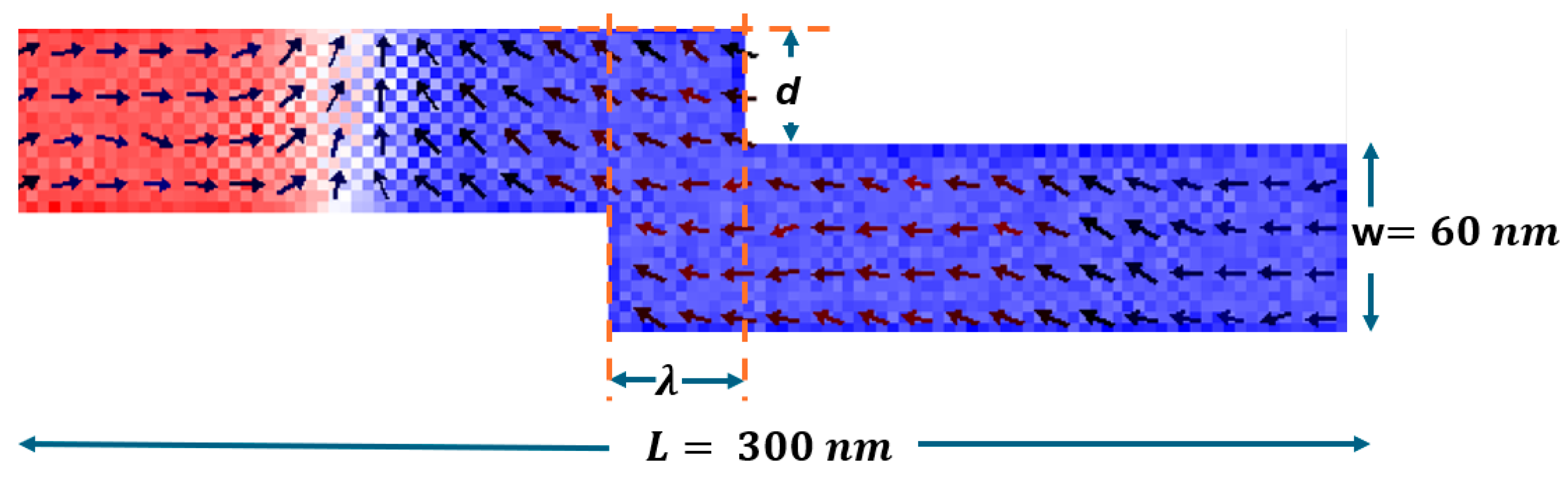
2. Modeling
3. Results and Discussion
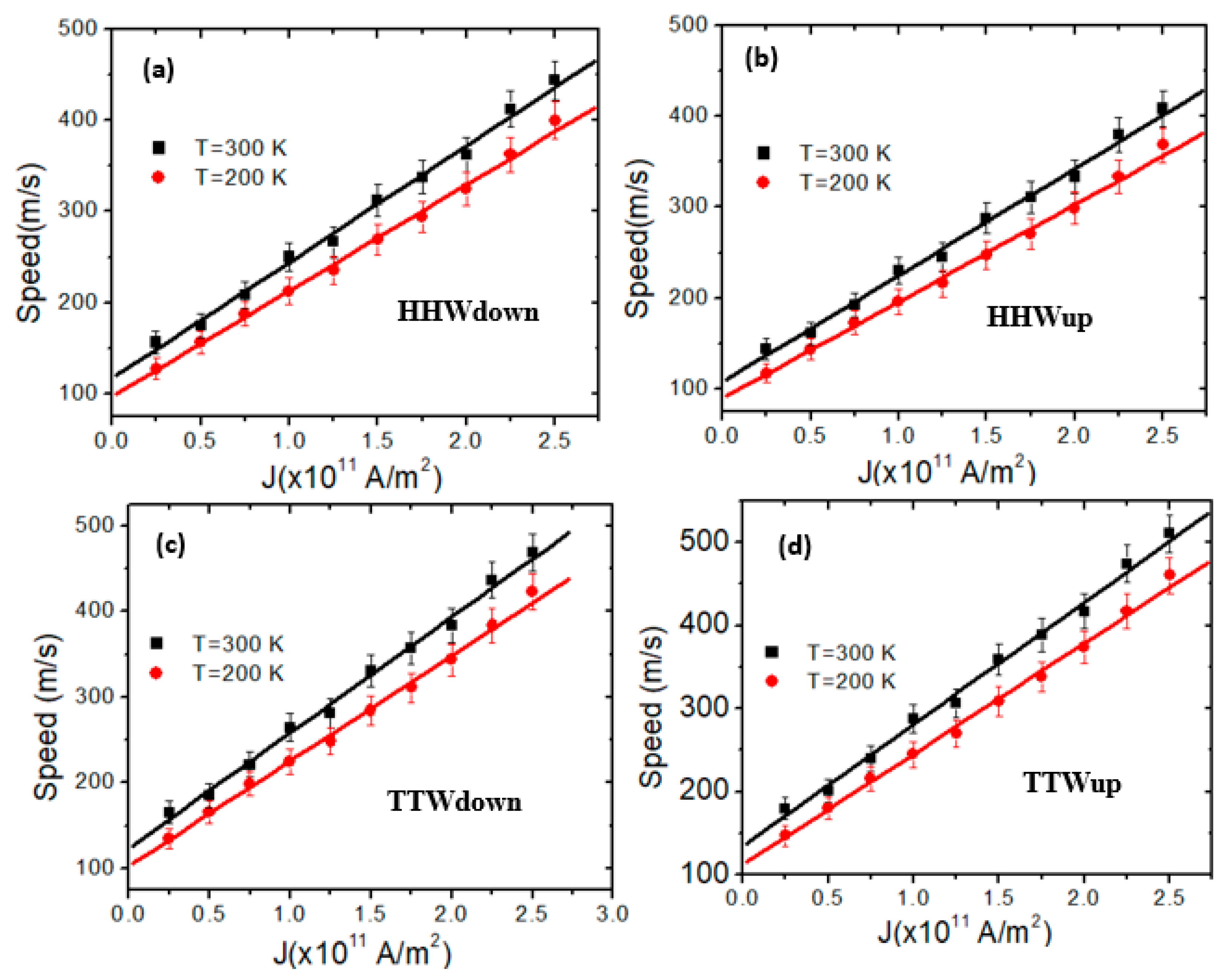
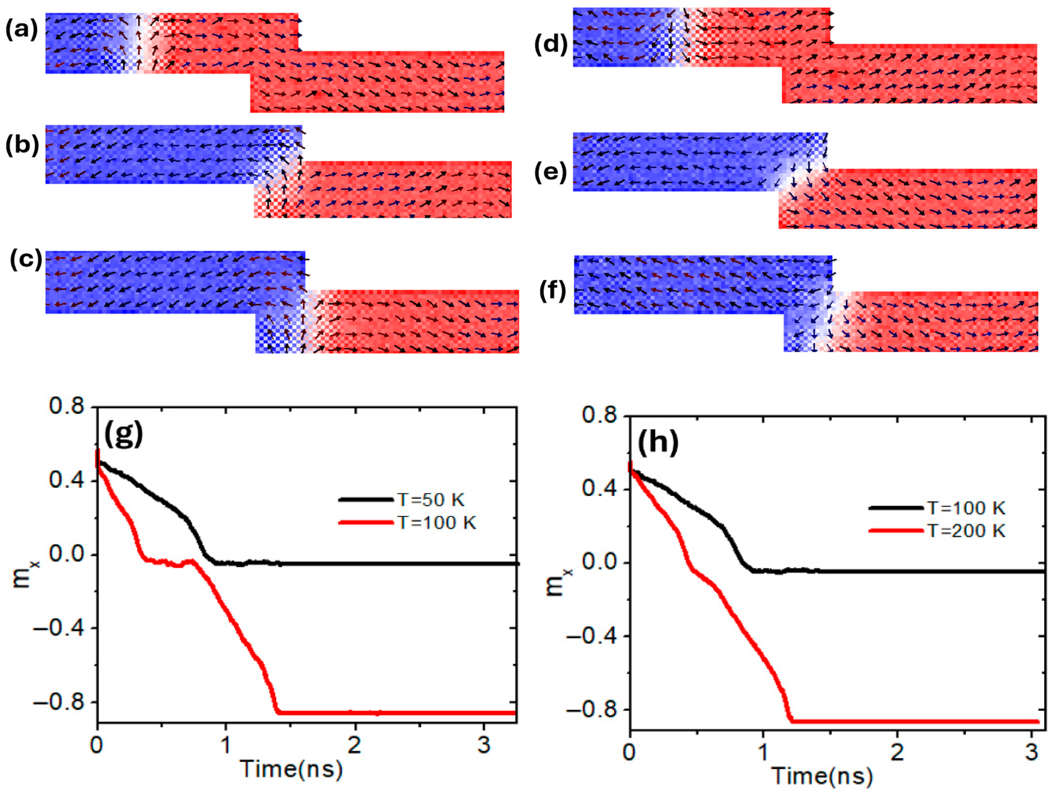
3.1. Chirality-Dependent Dynamics at Varying Temperatures
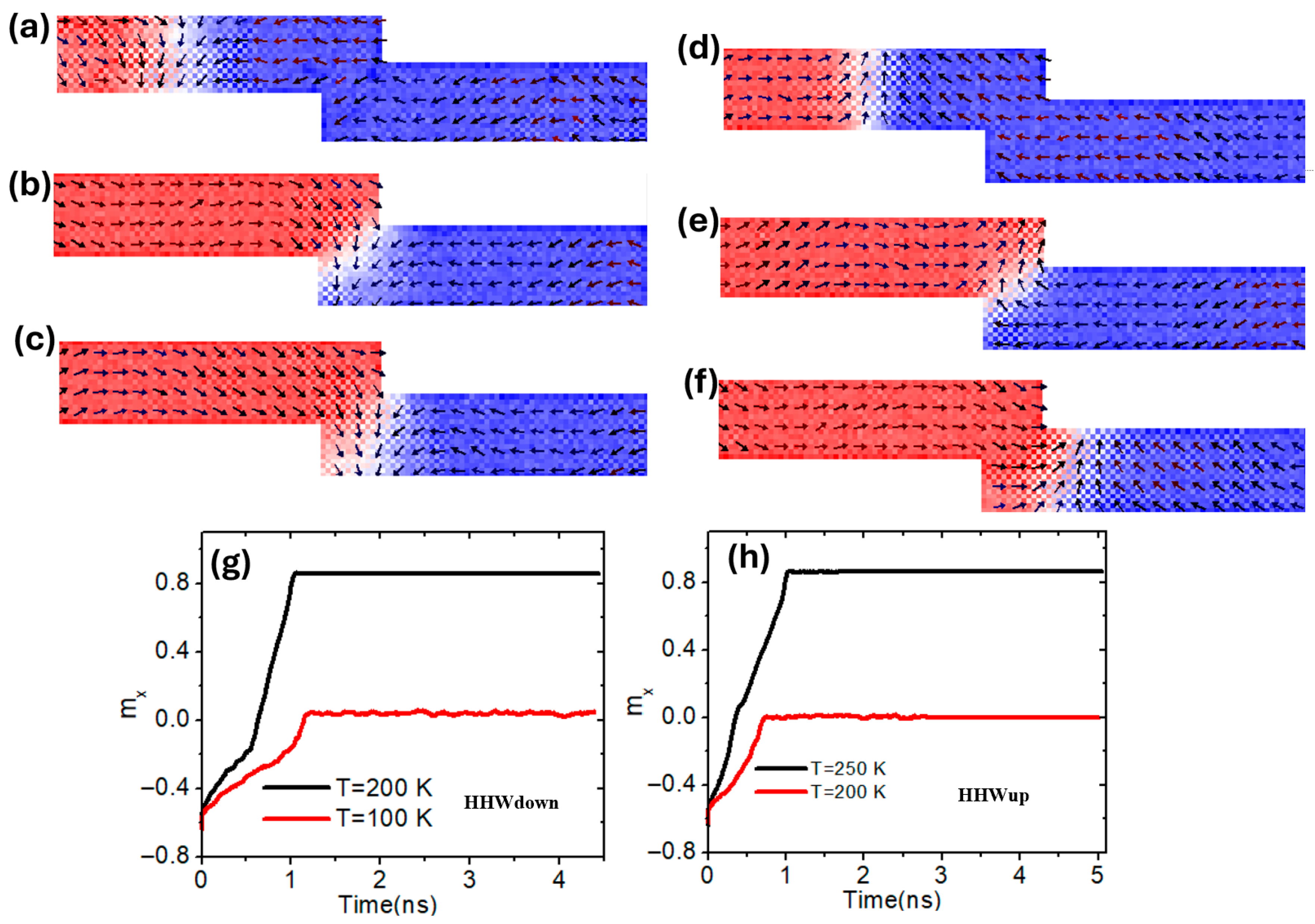
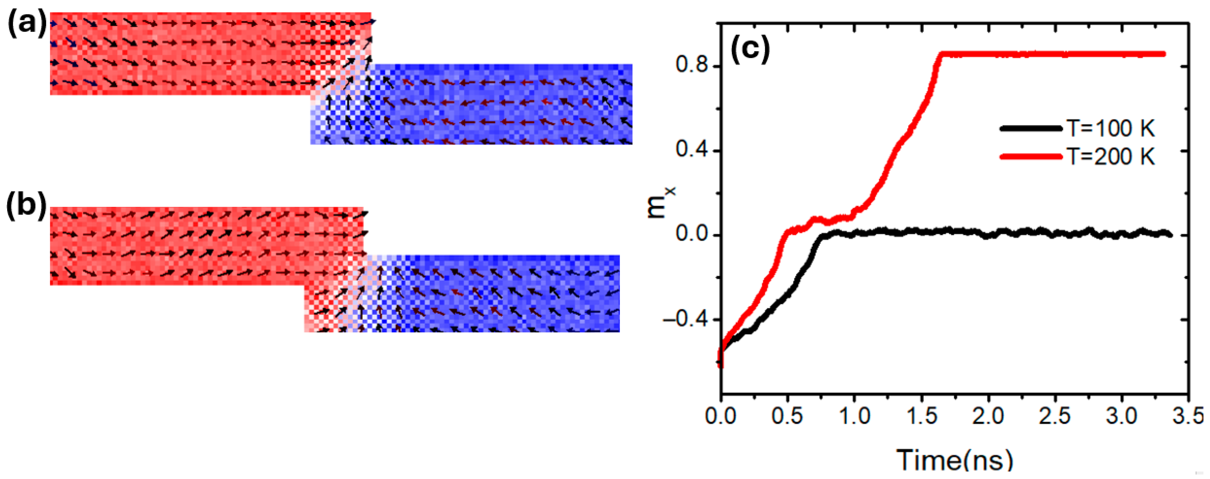
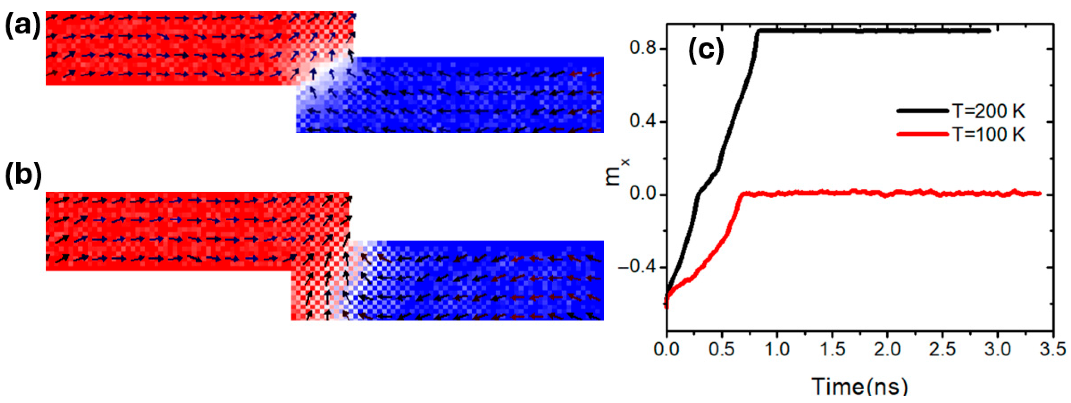
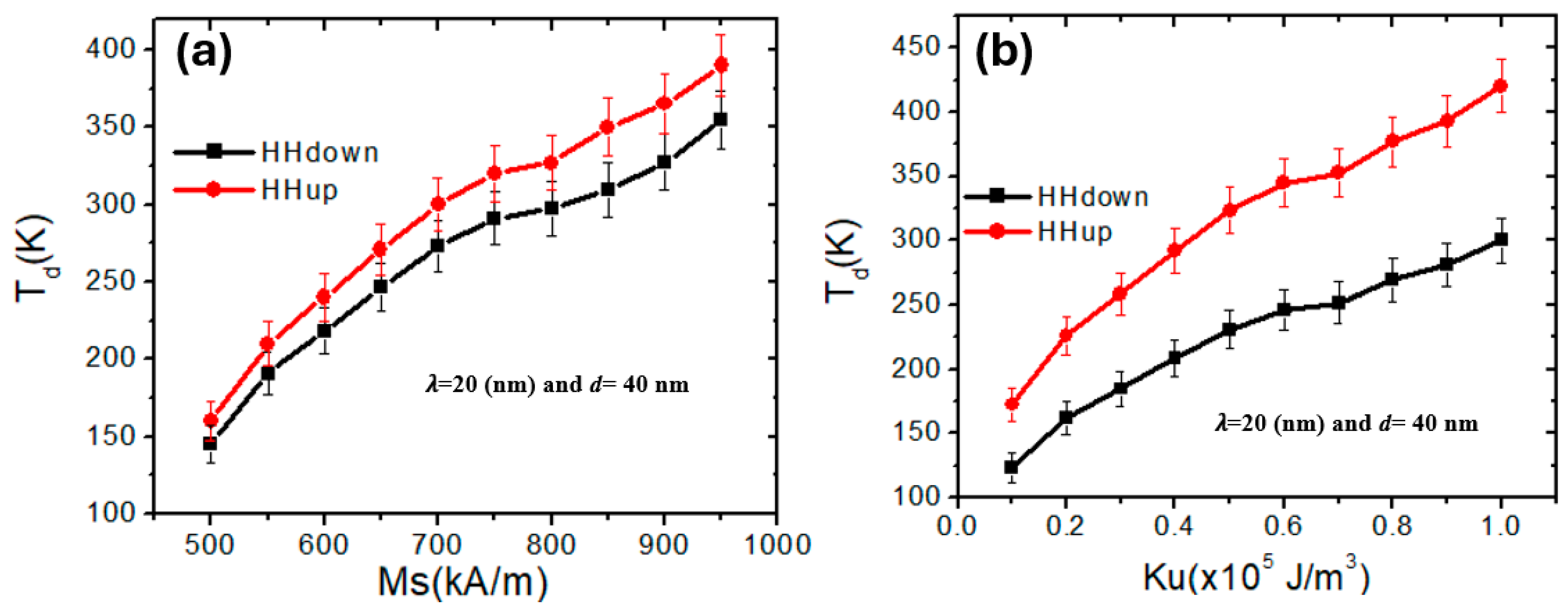
3.2. HHWup and HHWdown Thermal Pinning
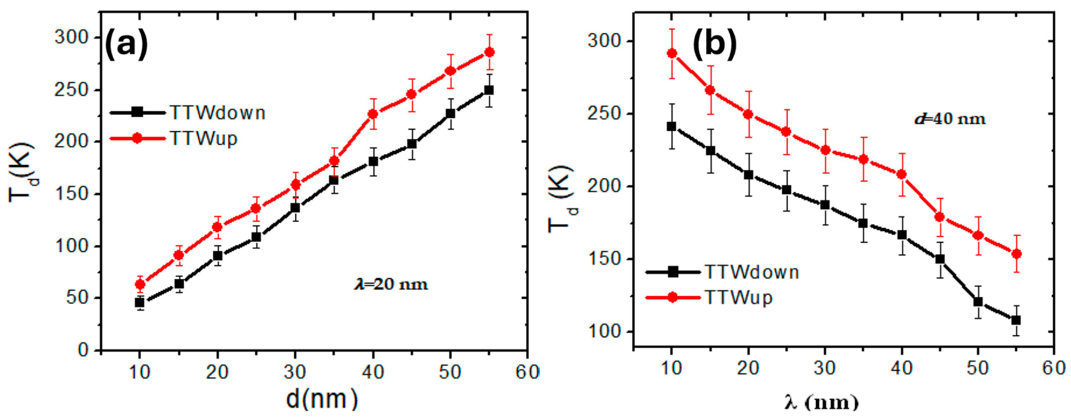
3.3. TTWup and TTWdown Pinning
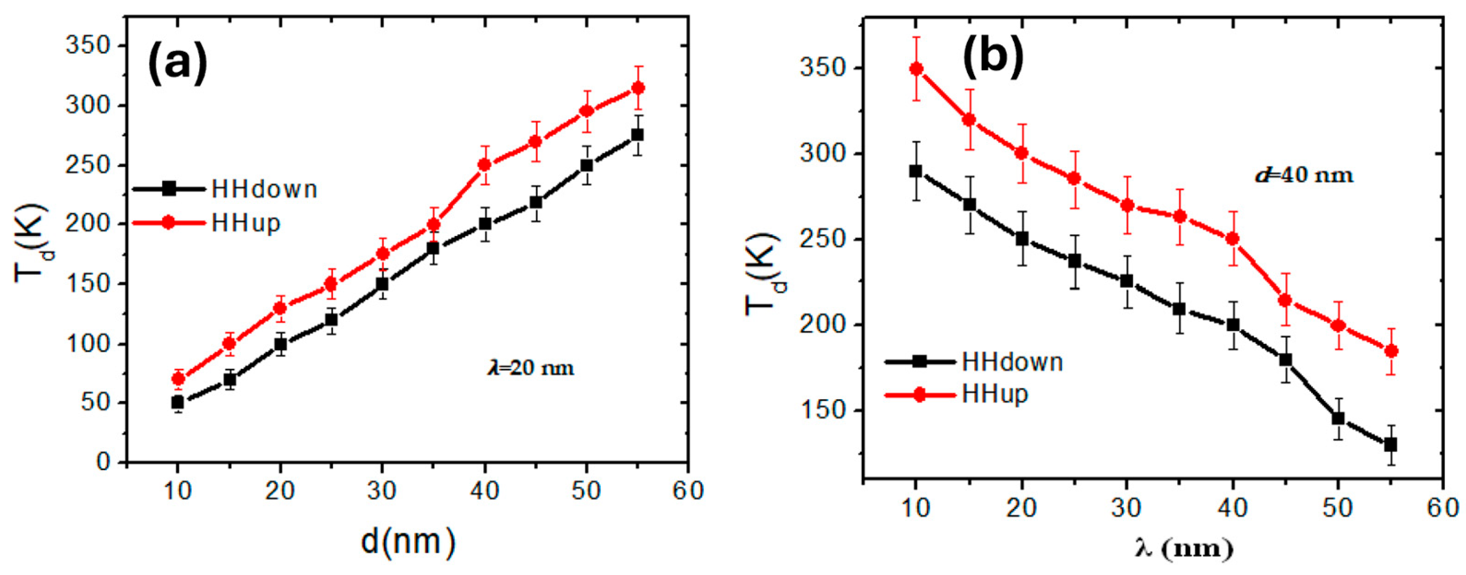
3.4. Magnetic Property Pinning and Depinning
4. Conclusions
Author Contributions
Funding
Data Availability Statement
Conflicts of Interest
References
- Berger, L. Exchange Interaction and Domain Wall Motion in Magnetic Nanostructures. Phys. Rev. B 1996, 54, 9353–9358. [Google Scholar] [CrossRef] [PubMed]
- Hayashi, M.; Thomas, L.; Moriya, R.; Rettner, C.; Parkin, S.S.P. Current-Controlled Magnetic Domain-Wall Nanowire Shift Register. Science 2008, 320, 209–211. [Google Scholar] [CrossRef] [PubMed]
- Junginger, F.; Kläui, M.; Backes, D.; Rüdiger, U.; Kasama, T.; Dunin-Borkowski, R.E.; Heyderman, L.J.; Vaz, C.A.F.; Bland, J.A.C. Spin Torque and Heating Effects in Current-Induced Domain Wall Motion Probed by Transmission Electron Microscopy. Appl. Phys. Lett. 2007, 90, 132506. [Google Scholar] [CrossRef]
- You, C.Y. Concept of the Field-Driven Domain Wall Motion Memory. J. Magn. Magn. Mater. 2009, 321, 888–890. [Google Scholar] [CrossRef]
- Zhao, W.S.; Duval, J.; Ravelosona, D.; Klein, J.O.; Kim, J.V.; Chappert, C. A compact model of domain wall propagation for logic and memory design. J. Appl. Phys. 2011, 109, 07D501. [Google Scholar] [CrossRef]
- Bryan, M.T.; Bance, S.; Dean, J.; Schrefl, T.; Allwood, D.A. Transverse and vortex domain wall structure in magnetic nanowires with uniaxial in-plane anisotropy. J. Phys. Condens. Matter 2012, 24, 024205. [Google Scholar] [CrossRef]
- Rottmayer, R.; Batra, S.; Buechel, D.; Challener, W.; Hohlfeld, J.; Kubota, Y.; Li, L.; Lu, B.; Mihalcea, C.; Mountfield, K.; et al. Heat-Assisted Magnetic Recording. IEEE Trans. Magn. 2006, 42, 2417–2421. [Google Scholar] [CrossRef]
- Al Bahri, M. Vortex domain wall dynamics in stepped magnetic nanowire with in-plane magnetic anisotropy. J. Magn. Magn. Mater. 2020, 515, 167293. [Google Scholar] [CrossRef]
- Choi, Y.S.; Lee, J.Y.; Yoo, M.W.; Lee, K.S.; Guslienko, K.Y.; Kim, S.K. Critical nucleation size of vortex core for domain wall transformation in soft magnetic thin film nanostrips. Phys. Rev. B 2009, 80, 012402. [Google Scholar] [CrossRef]
- Tsai, J.-L.; Huang, J.-C.; Tai, H.-W.; Tsai, W.-C.; Lin, Y.-C. Magnetic properties and microstructure of FePtB, FePt(B–Ag) granular films. J. Magn. Magn. Mater. 2013, 329, 6–13. [Google Scholar] [CrossRef]
- Al Bahri, M. Geometrical confinement of vortex domain wall in constricted magnetic nanowire with in-plane magnetic anisotropy. IEEE Trans. Magn. 2021, 57, 1–7. [Google Scholar] [CrossRef]
- Beach, G.S.D.; Tsoi, M.; Erskine, J.L. Current-induced domain wall motion. J. Magn. Magn. Mater. 2008, 320, 1272–1281. [Google Scholar] [CrossRef]
- Yang, S.M.; Yoon, J.-G.; Noh, T.W. Nanoscale studies of defect-mediated polarization switching dynamics in ferroelectric thin film capacitors. Curr. Appl. Phys. 2011, 11, 1111–1125. [Google Scholar] [CrossRef]
- Bansal, S.; Kumar, S.; Jain, A.; Rohilla, V.; Prakash, K.; Gupta, A.; Ali, T.; Alenezi, A.M.; Islam, M.S.; Soliman, M.S.; et al. Design and TCAD analysis of few-layer graphene/ZnO nanowires heterojunction-based photodetector in UV spectral region. Sci. Rep. 2025, 15, 7762. [Google Scholar]
- Zhou, Y.; Hu, C.; Zhang, Y. Current-induced vortex domain wall depinning in ferromagnetic nanowires with artificial linear defects. Appl. Phys. A 2015, 121, 297–300. [Google Scholar] [CrossRef]
- Kunz, A.; Rentsch, E. Simulations of field driven domain wall interactions in ferromagnetic nanowires. IEEE Trans. Magn. 2010, 46, 1556–1558. [Google Scholar] [CrossRef]
- Kunz, A.; Reiff, S. Enhancing domain wall speed in nanowires with transverse magnetic fields. J. Appl. Phys. 2008, 103, 07D903. [Google Scholar] [CrossRef]
- Al Bahri, M.; Al-Kamiyani, S. Harnessing magnetic properties for precision thermal control of vortex domain walls in constricted nanowires. Nanomaterials 2025, 15, 372. [Google Scholar] [CrossRef]
- Li, Z.; Zhang, S. Domain-wall dynamics driven by adiabatic spin-transfer torques. Phys. Rev. B 2004, 70, 024417. [Google Scholar] [CrossRef]
- Eastwood, D.S.; King, J.A.; Bogart, L.K.; Cramman, H.; Atkinson, D. Chirality-dependent domain wall pinning in a multinotched planar nanowire and chirality preservation using transverse magnetic fields. J. Appl. Phys. 2011, 109, 013903. [Google Scholar] [CrossRef]
- Al Bahri, M.; Al-Kamiyani, S. Thermal effects on domain wall stability at magnetic stepped nanowire for nanodevices storage. Nanomaterials 2024, 14, 1202. [Google Scholar] [CrossRef]
- Brandão, J.; Novak, R.L.; Lozano, H.; Soledade, P.R.; Mello, A.; Garcia, F.; Sampaio, L.C. Control of the magnetic vortex chirality in Permalloy nanowires with asymmetric notches. J. Appl. Phys. 2014, 116, 193902. [Google Scholar] [CrossRef]
- Paixão, E.; Toscano, D.; Gomes, J.; Leonel, S.A.; Coura, P.Z. Depinning of the transverse domain wall trapped at magnetic impurities patterned in planar nanowires: Control of the wall motion using low-intensity and short-duration current pulses. J. Magn. Magn. Mater. 2018, 451, 639–646. [Google Scholar] [CrossRef]
- Leliaert, J.; Van de Wiele, B.; Vandermeulen, J.; Coene, A.; Vansteenkiste, A.; Laurson, L.; Durin, G.; Van Waeyenberge, B.; Dupré, L. Thermal effects on transverse domain wall dynamics in magnetic nanowires. Appl. Phys. Lett. 2015, 106, 202401. [Google Scholar] [CrossRef]
- Bansal, S.; Prakash, K.; Sharma, K.; Sardana, N.; Kumar, S.; Gupta, N.; Singh, A.K. A highly efficient bilayer graphene/ZnO/silicon nanowire based heterojunction photodetector with broadband spectral response. Nanotechnology 2020, 31, 405205. [Google Scholar] [CrossRef]
- Bogart, L.; Eastwood, D.; Atkinson, D. The effect of geometrical confinement and chirality on domain wall pinning behavior in planar nanowires. Appl. Phys. Lett. 2008, 104, 033904. [Google Scholar] [CrossRef]
- Al Bahri, M.; Al Hinaai, M.; Al Balushi, R.; Al-Kamiyani, S. Enhancing the thermal stability of skyrmion in magnetic nanowires for nanoscale data storage. Nanomaterials 2024, 14, 1763. [Google Scholar] [CrossRef]
- Martinez, E.; Lopez-Diaz, L.; Torres, L.; Tristan, C.; Alejos, O. Thermal effects in domain wall motion: Micromagnetic simulations and analytical model. Phys. Rev. B 2007, 75, 174409. [Google Scholar] [CrossRef]
- Zhang, S.; Li, Z. Roles of nonequilibrium conduction electrons on the magnetization dynamics of ferromagnets. Phys. Rev. Lett. 2004, 93, 127204. [Google Scholar] [CrossRef]
- Al Bahri, M.; Borie, B.; Jin, T.L.; Sbiaa, R.; Kläui, M.; Piramanayagam, S.N. Staggered magnetic nanowire devices for effective domain-wall pinning in racetrack memory. Phys. Rev. Appl. 2019, 11, 024023. [Google Scholar] [CrossRef]
- Narayanapillai, K.; Qiu, X.; Rhensius, J.; Yang, H. Thermally assisted domain wall nucleation in perpendicular anisotropy trilayer nanowires. J. Phys. D Appl. Phys. 2014, 47, 105005. [Google Scholar] [CrossRef]
- Kurniawan, C.; Djuhana, D. Current driven domain wall depinning in notched Permalloy nanowires. AIP Conf. Proc. 2016, 1711, 020001. [Google Scholar] [CrossRef]
- Fukami, S.; Ieda, J.; Ohno, H. Thermal stability of a magnetic domain wall in nanowires. Phys. Rev. B 2015, 91, 235401. [Google Scholar] [CrossRef]
- de Vries, J.; Bolhuis, T.; Abelmann, L. Temperature dependence of the energy barrier and switching field of sub-micron magnetic islands with perpendicular anisotropy. New J. Phys. 2017, 19, 093019. [Google Scholar] [CrossRef]
- Saavedra, E.; Vidal-Silva, N.; Escrig, J. Dynamic Susceptibility of Permalloy Wire-Tube Nanostructures. Results Phys. 2021, 31, 104874. [Google Scholar] [CrossRef]
- Dao, N.; Donahue, M.J.; Dumitru, I.; Spinu, L.; Whittenburg, S.L.; Lodder, J.C. Dynamic Susceptibility of Nanopillars. Nanotechnology 2004, 15, S634–S638. [Google Scholar] [CrossRef]
- Pal, P.K.; Majumder, S.; Otani, Y.; Barman, A. Bias-Field Tunable Magnon–Magnon Coupling in Ni80Fe20 Nanocross Array. Adv. Quantum Technol. 2023, 6, 2300003. [Google Scholar] [CrossRef]
- Donahue, M.; Porter, D.G. “OOMMF User’s Guide, Version 1.0, Interagency Report NISTIR 6376; Technical 427 Report”, Version 1.0; National Institute of Standards and Technology: Gaithersburg, MD, USA, 1999. Available online: https://math.nist.gov/oommf/ (accessed on 6 June 2025).
- Al Bahri, M. Controlling domain wall thermal stability switching in magnetic nanowires for storage memory nanodevices. J. Magn. Magn. Mater. 2022, 543, 168611. [Google Scholar] [CrossRef]
- Brown, W.F., Jr. Thermal Fluctuations of a Single-Domain Particle. Phys. Rev. 1963, 130, 1677–1686. [Google Scholar] [CrossRef]
- Gupta, S.; Sbiaa, R.; Al Bahri, M.; Ghosh, A.; Piramanayagam, S.N.; Ranjbar, M.; Akerman, J. [Co/Ni] multilayers with robust post-annealing performance for spintronics device applications. J. Phys. D Appl. Phys. 2018, 51, 465002. [Google Scholar] [CrossRef]

Disclaimer/Publisher’s Note: The statements, opinions and data contained in all publications are solely those of the individual author(s) and contributor(s) and not of MDPI and/or the editor(s). MDPI and/or the editor(s) disclaim responsibility for any injury to people or property resulting from any ideas, methods, instructions or products referred to in the content. |
© 2025 by the authors. Licensee MDPI, Basel, Switzerland. This article is an open access article distributed under the terms and conditions of the Creative Commons Attribution (CC BY) license (https://creativecommons.org/licenses/by/4.0/).
Share and Cite
Al Bahri, M.; Al-Kamiyani, S.; Al Hinaai, M.M.; Ali, N. Thermal Influence on Chirality-Driven Dynamics and Pinning of Transverse Domain Walls in Z-Junction Magnetic Nanowires. Symmetry 2025, 17, 1184. https://doi.org/10.3390/sym17081184
Al Bahri M, Al-Kamiyani S, Al Hinaai MM, Ali N. Thermal Influence on Chirality-Driven Dynamics and Pinning of Transverse Domain Walls in Z-Junction Magnetic Nanowires. Symmetry. 2025; 17(8):1184. https://doi.org/10.3390/sym17081184
Chicago/Turabian StyleAl Bahri, Mohammed, Salim Al-Kamiyani, Mohammed M. Al Hinaai, and Nisar Ali. 2025. "Thermal Influence on Chirality-Driven Dynamics and Pinning of Transverse Domain Walls in Z-Junction Magnetic Nanowires" Symmetry 17, no. 8: 1184. https://doi.org/10.3390/sym17081184
APA StyleAl Bahri, M., Al-Kamiyani, S., Al Hinaai, M. M., & Ali, N. (2025). Thermal Influence on Chirality-Driven Dynamics and Pinning of Transverse Domain Walls in Z-Junction Magnetic Nanowires. Symmetry, 17(8), 1184. https://doi.org/10.3390/sym17081184