1. Introduction
In recent years, Buck converters have been widely deployed in renewable energy systems, electric vehicles, fuel cells, explosion-proof power supplies, aerospace power units, defense applications, and information-industry (IT) systems. High efficiency, high power density, high reliability, better transient response, and low electromagnetic interference (EMI) remain enduring design goals for Buck converters, such as an inductor Buck converter [
1,
2,
3,
4]. Representative approaches include a dual-operating mode control technique introduced to enhance transient response [
1]; a peak/valley current mode control method presented to precisely regulate output voltage [
2]; an automatic mode switching scheme that ensures robust operation and suppresses EMI in high duty ratios [
3]; and a synchronous Buck converter with a coupled inductor that achieves zero voltage switching (ZVS) [
4].
For further improving power density and switching frequency while reducing current ripple, the interleaved Buck topology has attracted widespread attention. Interleaved Buck converters are typically implemented as (i) series-capacitor Buck converters, (ii) multiphase Buck converters with discrete inductors, or (iii) multiphase Buck converters employing coupled inductors.
Series capacitor Buck converters (SC Buck) [
5,
6,
7,
8] have also been extensively explored to improve operating frequency, improve system dynamics, reduce component stress, and share of current. However, the SC Buck circuit structure is more complicated than that of a discrete inductor multiphase Buck converter. To achieve a high output current, multiphase Buck converters with discrete inductors have been investigated [
9,
10,
11]. For example, in electrical vehicles, the digital control deployed in FPGA used in the bidirectional interleaved Buck converter [
9] and the feedback matrix design [
10] are given to simplify the design of the controller, and the multiphase Buck converter based on current control of the synchronization of zero-crossing current ripples [
11] overcome high-dynamic and high-power issues.
However, interleaved Buck converters that employ discrete inductors require active current-sharing control among phases. In addition, the triangular inductor current also has bad effects, and the control circuit consisting of analog devices will be very complex because its duty cycle is usually between 0 and 1.
Therefore, multiphase Buck converters employing inductors, either inversely or positively coupled, have been widely studied and applied. Positively coupled inductors have also been adopted in other high-efficiency paralleling schemes, where the positive coupling is exploited to redistribute current and shape switching transitions [
12]. Positively coupled inductors have also been adopted in other high-efficiency paralleling schemes, where positive coupling is exploited to redistribute current and shape switching transitions [
13]. Inversely coupled multiphase Buck converters can effectively improve efficiency and have fast transient responses [
14,
15,
16], but there is an oscillation phenomenon and a larger equivalent coupling inductor when the procedure occurs, which will extend the coupling time. Beyond inversely coupled structures, interleaved buck-type topologies employing coupled inductors have also been explored for voltage balancing in bipolar DC microgrids, where the emphasis is on balancing performance rather than extending duty-cycle range or achieving ZVS/ZCS in DCM/CCM hybrid operation [
17]. Furthermore, there is a coupled multiphase Buck converter [
18,
19,
20], whose power devices can operate in zero-voltage switching (ZVS) in continuous conduction mode (CCM), but the resulting second-order dynamics complicates the design of the controller parameter.
Building on previous work on high-gain step-up converters employing coupled inductors, including our earlier design of a non-isolated high-gain step-up DC–DC converter with reduced voltage stresses [
21], this paper focuses on a step-down two-phase interleaved Buck topology with positively coupled inductors.
In this paper, two investigate an interleaved Buck converter employing a positively coupled inductor. The converter is configured so that magnetic coupling occurs during switching transitions, while the phase currents in the individual inductors operate in discontinuous conduction mode (DCM) and their sum remains in continuous conduction mode (CCM). The topology is tailored to meet the stable power supply requirements of modern electronic products. The main contributions of this paper can be summarized as follows.
A two-phase interleaved Buck converter with positively coupled inductors is proposed, in which the phase currents operate in DCM and their sum remains in CCM. By appropriately timing the magnetic coupling during switching transitions, all main power devices achieve ZVS and ZCS, thereby reducing switching losses without the need for auxiliary switches or resonant networks.
The proposed architecture extends the effective duty cycle range and achieves a conversion ratio higher than that of conventional interleaved Buck converters, without resorting to extreme duty cycles, facilitating a high conversion ratio and high-power density while maintaining a relatively simple control structure.
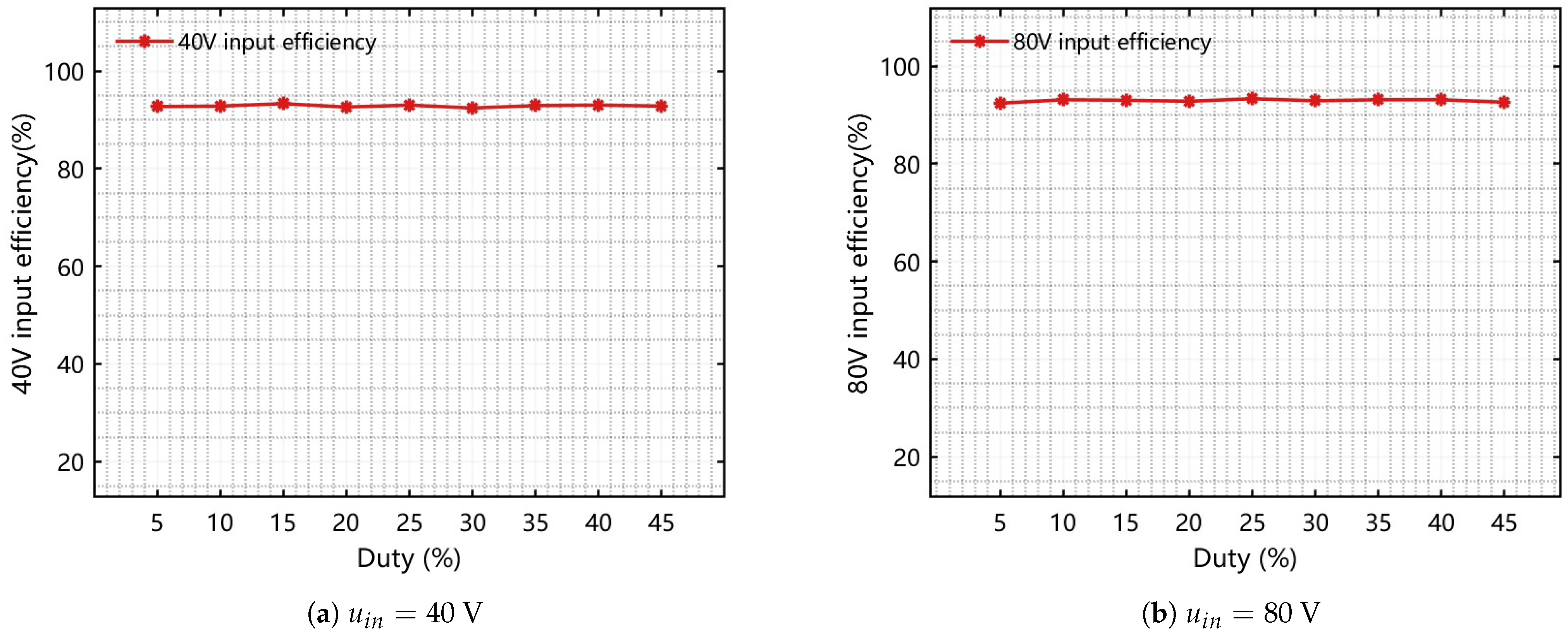
Compared with conventional interleaved Buck converters with discrete inductors, shaped inductor current waveforms exhibit reduced ripple and improved inherent current sharing between phases. The experimental 270W prototype demonstrates a peak efficiency of 93.3% at a conversion ratio of 0.5, confirming that the proposed positively coupled structure provides a significant advance over existing interleaved and coupled-inductor Buck designs.
The remainder of this manuscript is organized as follows. In
Section 2, the topology and the control requirement are discussed in detail. In
Section 3, the magnetic coupling interval is presented in CCM. In
Section 4, the operating principle of CCM is analyzed. In
Section 5, the relationship between the output-input voltages and the performances are given. In
Section 6 presents the signal model. In
Section 7, we summarize the advantages and disadvantages of the mentioned topologies compared to other topologies. Furthermore,
Section 8 reports on the simulation results. The experimental results are given in
Section 9. Finally,
Section 10 concludes this paper.
2. System Configuration of Two-Phase Interleaved Buck Converter
In this paper, a high-conversion ratio Two-Phase Interleaved Buck Converter with a Coupling Inductor topology is proposed, which focuses on the positively coupled inductor and the interleaved parallel connection. Among these, coupled inductors help to improve efficiency. The realization of this efficient energy transfer is closely related to the time-varying interaction of the magnetic and electric fields inside the converter, and the symmetry features inherent in this process are particularly crucial. The two-phase interleaved parallel structure optimizes the current ripple characteristics through the time symmetry in phase (the symmetrical timing of the two-phase interleaved operation), while the symmetrical design of the coupled inductor promotes the symmetrical coupling of the magnetic and electric fields. The two work together to reduce the asymmetric losses in the energy transfer process, providing a symmetrical basis for efficient operation.
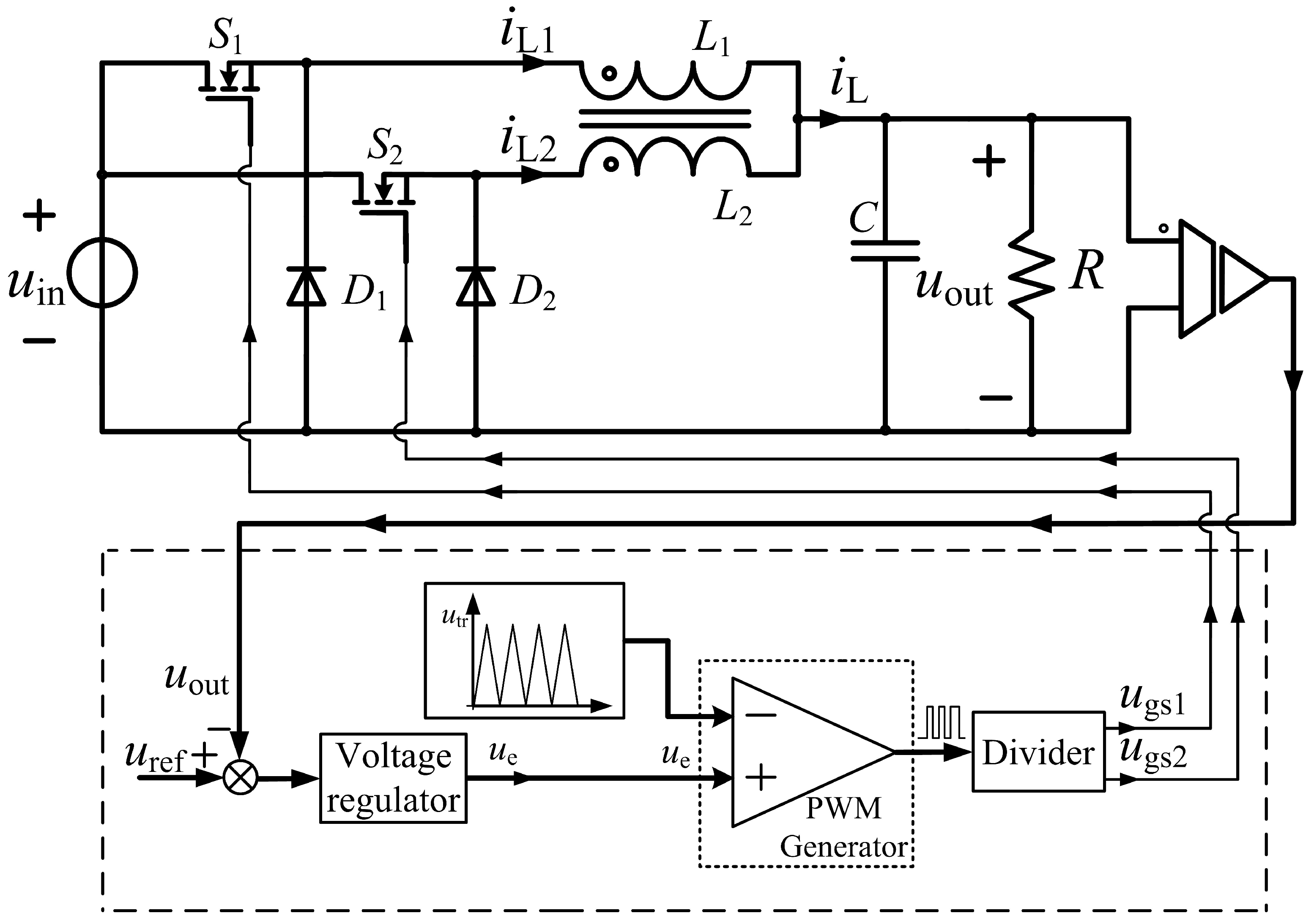
The circuit topology adopted in this work is illustrated in
Figure 1. The proposed topology may be divided into two functional units: (a) the positively coupled-inductor structure. (b) Interleaved Two-phases. Including coupled inductance (
L), two MOSFETs (
,
), two diodes (
,
), one capacitor (
C) and a load
R.Where
,
,
,
and
are the phase inductors, the currents in the phase inductors and the sum of the currents, respectively.
and
denote the input and output voltages, respectively. The diodes
and
, together with the MOSFET switching transistors
and
, enable the total inductor current to operate in continuous-conduction mode (CCM). MOSFETs
and
operate in an interleaved manner.
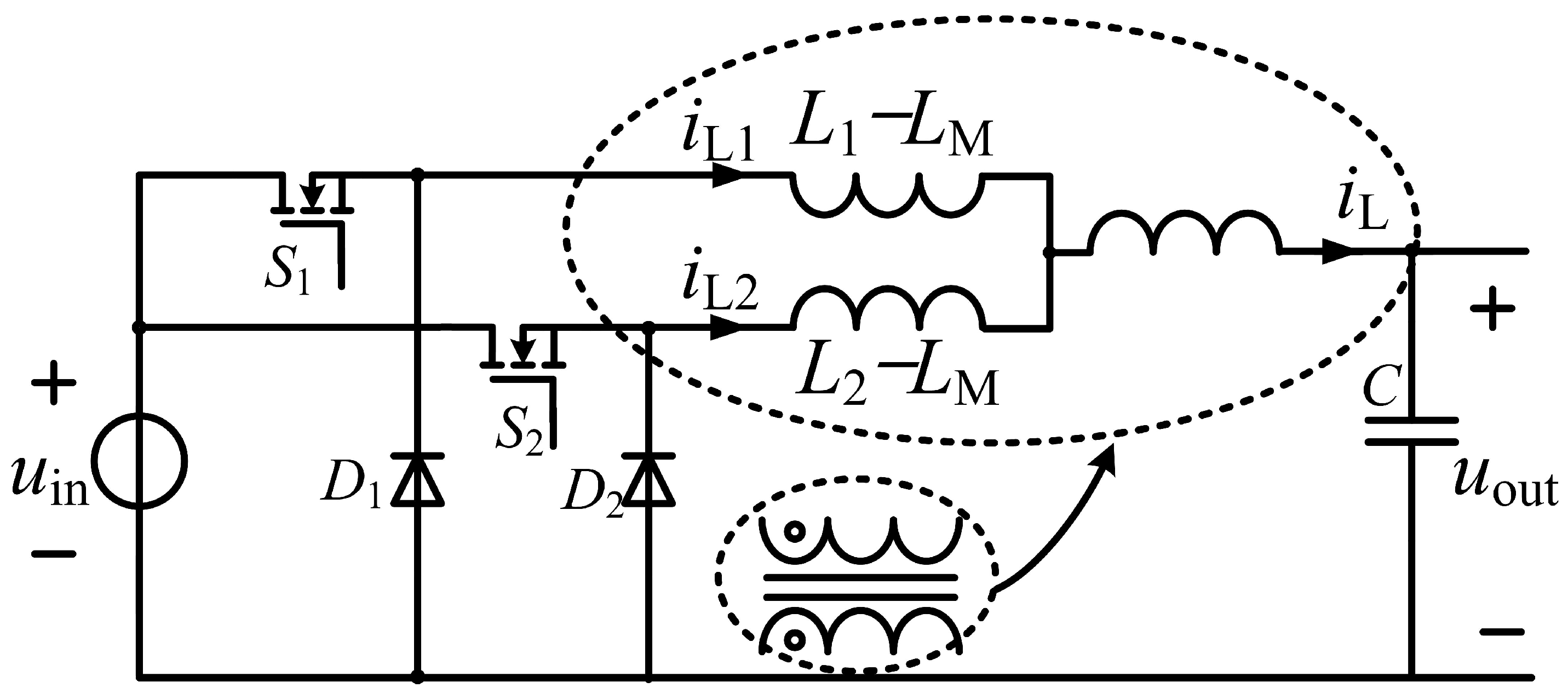
According to the model of a coupling inductor, the equivalent circuit of
Figure 1 is given again by
Figure 2 when the magnetic coupling interval of currents
and
occurs. Where
,
and
are mutual inductance and two leakage inductance, separately. Assuming
, the relationships of all inductances are demonstrated in detail in Equations (
1) and (
2), where k is the coupling coefficient. The current
is shown in Equation (
3) based on Kirchhoff’s Current Law (KCL).
Under steady-state conditions, one switching period is partitioned into six phases, as illustrated in
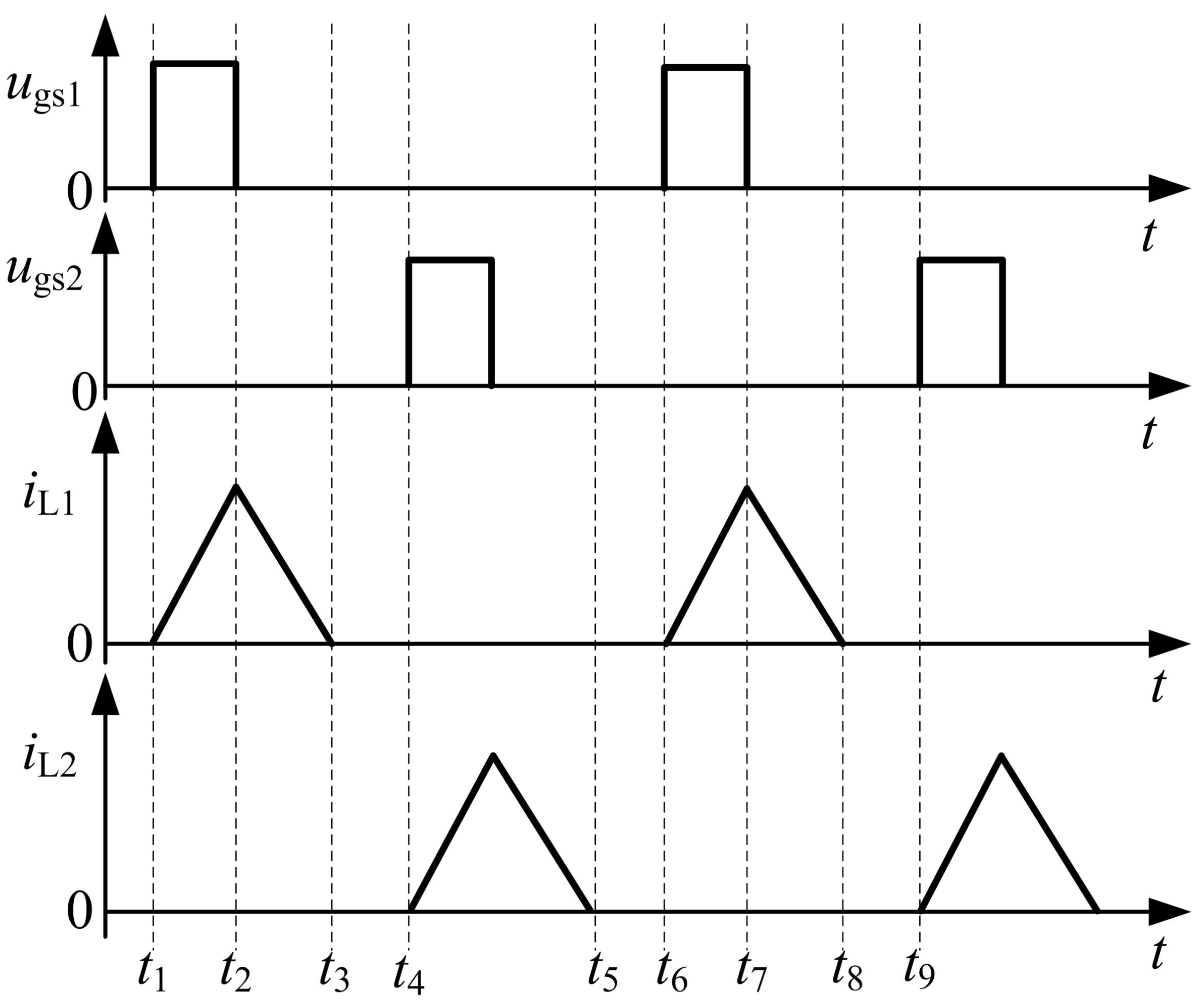
Figure 2. According to the aforementioned content, the main waveforms under CCM of the current
are shown in
Figure 3. Obviously, the state of the current
operates in the CCM under the magnetic coupling interval that occurs, as shown in
Figure 3. And at the same time, it is ensured that currents
and
must work in DCM in any case, where
,
,
, and
are the driving signals of MOSFETs
and
, the switching period, and the conducting time. During the time intervals
(
), the magnetic coupling interval of the currents
and
will appear.
The coupled inductor is realized on a single core leg, with the two windings wound bifilarly and having the same number of turns. The windings are tightly packed in adjacent layers, with short lead lengths and a single centralized air gap, so that almost all of the main flux is shared and the leakage flux is minimized. Under these conditions, the mutual inductance is very close to the geometric mean of the self-inductances (), and the coupling coefficient is therefore close to 1.
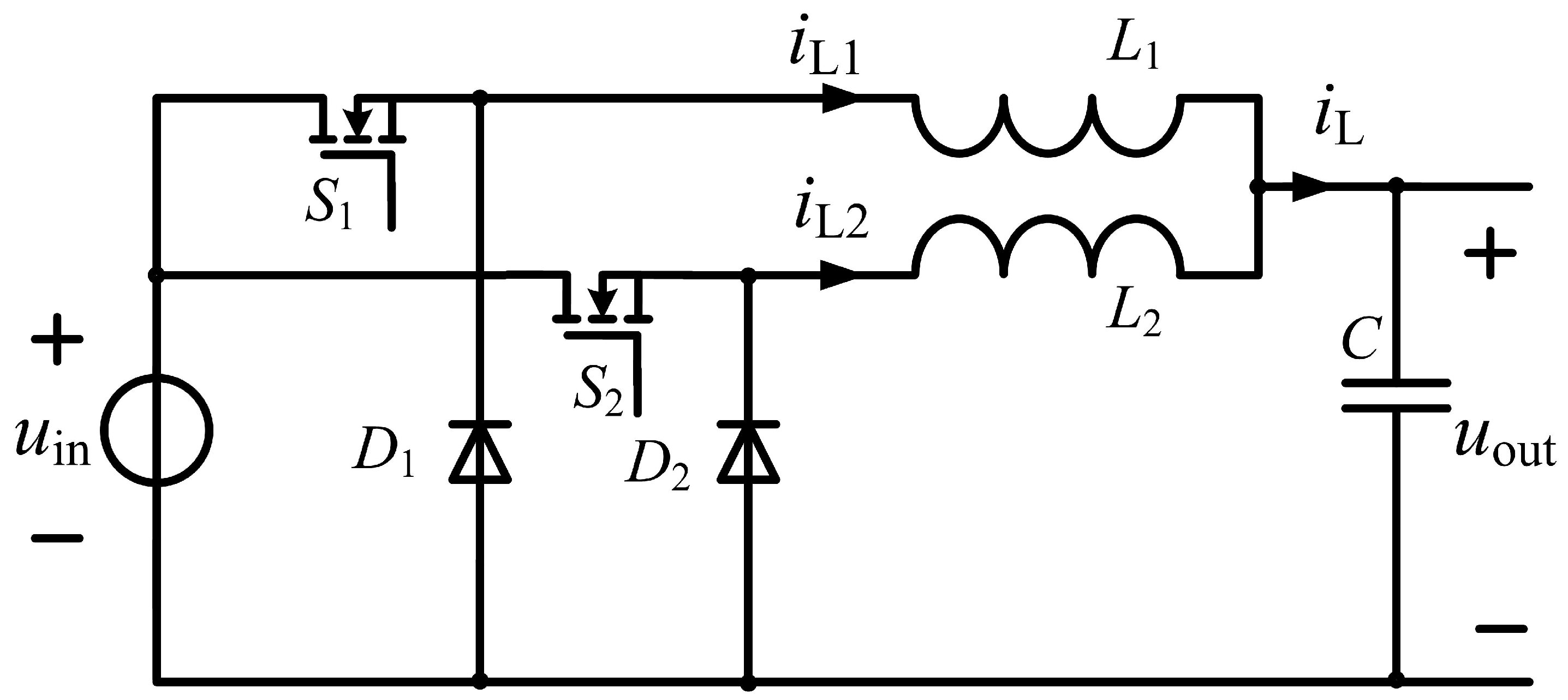
When the magnetically coupled interval is absent—that is,
and
do not interact—the power stage is reduced to the equivalent circuit in
Figure 4, and the representative waveforms are shown in
Figure 5. In this case, the operating principle is identical to that of a traditional two-phase interleaved Buck topology operated in DCM. As the underlying dynamics are standard and introduces no additional insight for the proposed topology, a detailed analysis is omitted, and the discussion henceforth focuses on the coupled case.
3. Magnetic Coupling Interval Analysis
At this stage, the switch experiences ZCS; the
diode remains reverse-biased and off. According to
Figure 3, the coupling procedure appears during the time interval (
). The corresponding equivalent circuit for power conversion appears in
Figure 6a. The relationships of voltage and current are expressed in Equation (
4). Equation (
5) is easily obtained by solving (
4). In the same way, Equation (
6) is also obtained during the time interval (
).
When the coefficient
k is close to 1, the
term in Equations (
5) and (
6) can be approximately equal to 0, that is, it can be further simplified to Equations (
7) and (
8).
Thus, it is clear that Equation (
9) is established from Equations (
7) and (
8). That is, current
can be regarded as a constant current source as the sum of
and
is effectively constant and can be modeled as a current source. But the time intervals
and
are very short because the leakage inductance value in Equation 2 is relatively small, which, together with the small equivalent capacitance at the switching node, results in a resonant frequency much higher than the switching frequency. Consequently, the corresponding coupling intervals occupy only a very small fraction of the switching period, and their influence on the average inductor current and conversion ratio can be safely ignored.
4. Operation Principle Under CCM Condition
The proposed converter employs two active switches in the power stage. Its operating principle is governed by the dynamic interaction between the gate-drive signals and the current flowing through the coupled inductor winding. Under steady-state conditions, each switching period is divided into six consecutive operating modes, as illustrated in
Figure 3, and the corresponding equivalent circuits for these modes are shown in
Figure 6.
State 1 (
). The switch and the switching diode achieve
ZCS in this state, and the diodes
are reverse cutoff. The equivalent circuit representing the power conversion path is shown in
Figure 6a. Before time
, the current
is zero and the current
follows through the diode
. At
, the upper MOSFET
is switched on with zero current. The current
and
starts to rise and decrease under voltage
until the current
increases to
at time
. At this time, the current
decreases to zero and the diode
is automatically turned off without reverse recovery. Because the coefficient k is close to 1, the current changing rate of
and
is relatively high. The slopes of the currents
and
can be considered as follows:
State 2 (
). In this state, the
self-inductance
network and Mutual induction
are charged. The equivalent circuit shown in
Figure 6b represents the power conversion path. The current
is equal to the current
. At this instant,
is turned off, while the diode remains reverse-biased and, therefore, non-conducting. Apparently, the current rate of change of
is smaller than that of Equation (
10) when the coefficient k is close to 1. This mode ends at
. Then, the currents
and
increase with a slope, which is described as follows:
State 3 (
). In this mode, the inductor discharges its stored energy, and
is acted as a freewheeling path. The equivalent circuit for power conversion is shown in
Figure 6c. The switches remain on and the diodes
are cut off in reverse. Currents
and
follow through the diode
under voltage
. At this time, the slope of the currents
and
is in the following form:
State 4 (
). This state is the stage where coupling occurs. An equivalent schematic for the power stage is provided in
Figure 6d. The diode
is on,
is off. The energy within the system is reallocated through the mutual inductance of the coupled inductors. At this time, the MOSFET
starts to work. Obviously, it is on with zero current because the current
is zero. Thus, the MOSFET
gets ZCS. From
, the currents
and
start to increase and decrease separately under voltage
until the current
increases to
at time
. At this moment, the current
decreases to zero, hence the diode
is automatically turned off without reverse recovery. That is,
obtains ZCS. Because the coefficient k is close to 1, the current changing rate of
and
is also relatively large. The slope of the current functions
and
is described below.
State 5 (
). In this state, the
self-inductance (
) network and Mutual induction (
) are charged. The power conversion equivalent circuit is depicted in
Figure 6e. With
continuously conducting, the diodes are reverse-biased and block current. During the time interval (
), the current changing rate of
is calculated using Equation (
14). It is clear that the rate of change of
is also smaller than that of Equation (
13) because the coefficient k is nearly 1. At
, the MOSFET
is turned off. At this time, the slope of the currents
and
can be given by Equation (
14).
State 6 (
). This state sets up the subsequent inductor energy-release phase, during which the current freewheels through
. The equivalent circuit representing the power conversion path is shown in
Figure 6f. All switching devices are off, and a diode
is used to move freely. Currents
and
follow through the diode
under voltage
, which is represented in Equation (
15). The next operating period will start from time
.
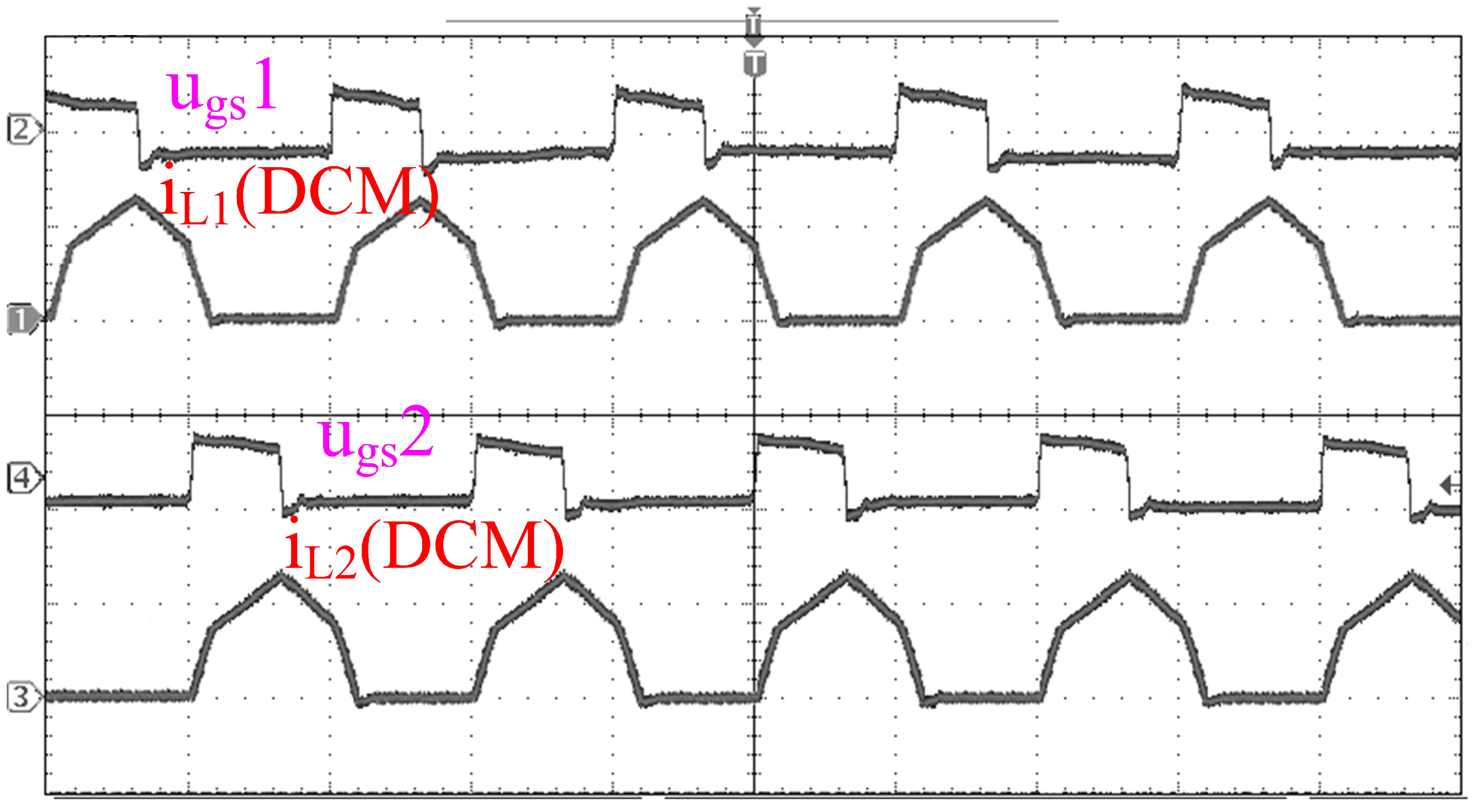
The converter operates through a multi-stage energy-exchange process over each switching period. During each cycle, the inductor current exhibits a periodic piecewise-linear waveform. Within each cycle, it initially maintains zero current, then rapidly rises, linearly rises to a peak, and rapidly falls back to zero current. The overall waveform resembles a cyclical “pulsed triangle wave”, exhibiting distinct piecewise-linear characteristics. The preparation of ZCS is performed by coupled inductance and diode renewal. The phases of the inductor currents and differ, demonstrating a periodic pattern of alternating operation. According to a previous analysis, MOSFETs and freewheeling diodes are found to operate in ZCS.
5. Converter Performance Analysis
For the considered DC–DC converter, the voltage conversion gain exhibits a linear dependence on the duty cycle
D. Since the currents of inductors
and
change periodically, we only analyze the change in inductor current of inductor
within one cycle. As shown in
Figure 3, the two duty cycles are defined by Equation (
16), respectively.
Here, D denotes the main duty cycle of the phase switches. In contrast, denotes the fraction of the switching period occupied by the coupling (commutation) intervals associated with the leakage inductance and the switch-node/device capacitances.
With regard to current
, only consider
. Thus, applying the volt-second balance to
in this interval gives Equation (
17) from
Figure 3. Therefore, the relationship between input and output voltages can be easily calculated as in Equation (
18). Similarly, for the current
, the input–output voltage relationship is identical to that given in Equation (
18).
According to
Figure 3 and Equation (
16), we have
. Since
and
are very short,
and hence
, so
can be neglected in the average model. Hence, the expression for the voltage gain in this mode is obtained by simplifying to Equation (
19).
The converter proposed in this paper realizes duty cycle expansion by magnetic coupling and a two-phase interleaved structure. The voltage gain achieves the change of the conventional Buck duty cycle between when the duty cycle D changes between . The limitation of conventional high-gain converters, which must operate near extreme duty cycles to cover a wide regulation range, is overcome.
6. Control System Design
The primary objective of the output voltage control loop is to regulate the output voltage and enhance the dynamic performance of the converter. The corresponding control block diagram is shown in
Figure 7. In this diagram,
denotes the reference output voltage;
denotes the small-signal transfer function that relates the main switch duty cycle
D to the average output voltage;
denotes the PI compensator;
represents the transfer function of the voltage detection stage; and
denotes the transfer function associated with the feedback path.
As shown in
Figure 7,
denotes the actual output voltage. Based on the small-signal model, the control-to-output (duty-to-voltage) transfer function is obtained and expressed in (
20) and (
21).
It is clear that using Equation (
20) to obtain that when
=0, the output voltage, as a function dependent on the input voltage, satisfies Equation (
22). It is equivalent to Equation (
19).
By combining the preceding results with Equation (
21), t, the transfer function
is given by Equation (
23).
Equation (
24) is the transfer function of the conventional single-inductor Buck output and duty cycle, which is the same as the new Buck transfer function in form.
For the voltage control loop, the compensator was designed on the basis of the small-signal control-to-output transfer function of the proposed converter. The plant transfer function was implemented in MATLAB. A robust PID-type controller was then tuned automatically using the pidtune command with a target phase margin of , prioritizing phase-margin robustness. This integral controller is adopted in the implementation of the voltage loop to regulate the output voltage and ensure zero steady-state error.
With parameter substitution, the system’s uncompensated open-loop transfer function yields the Bode plot computed in MATLAB R2024b.
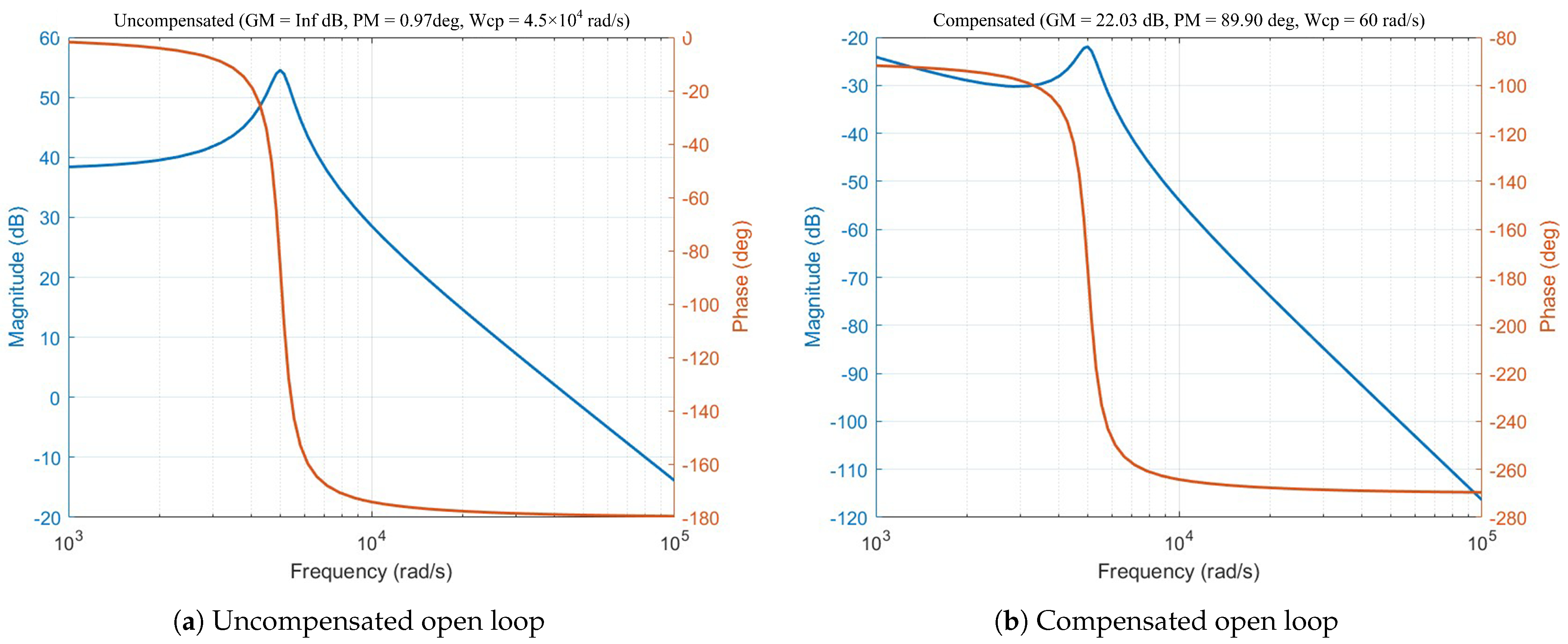
As indicated by
Figure 8a, the open-loop magnitude response has a shallow slope in the low-frequency range, which leads to a sluggish dynamic response. The phase margin is
, so the system has poor robustness and weak damping. A PI compensator is designed to stabilize the system and enhance its dynamics. The compensated transfer function is defined in
Figure 8b, and the corresponding Bode diagram is constructed from it.
With an infinite gain margin and a phase margin of , the compensated system satisfies the classical stability specifications and verifies the validity of the controller design.
10. Conclusions
This paper has presented a two-phase interleaved Buck converter employing a positively coupled inductor and operating in a DCM-per-phase but CCM-sum regime. The operating principle, soft-switching conditions, and design guidelines for the magnetic components and control parameters were analyzed in detail. A 270W laboratory prototype was built to validate the theoretical analysis.
Experimental waveforms confirm that the main power devices can achieve zero-current (and near zero-voltage) switching over the intended operating range, which effectively reduces switching losses. Because of the proposed current-shaping mechanism and positively coupled structure, the effective duty cycle range is extended, and a higher voltage conversion ratio is obtained compared with a conventional interleaved Buck converter at similar duty cycles. The prototype achieves a maximum efficiency of 93.3% with a conversion ratio of 0.5, demonstrating that the proposed topology can simultaneously realize high efficiency and a high conversion ratio with a relatively simple hardware implementation and control scheme.
Future work will focus on a more detailed characterization of electromagnetic interference and grounding effects, as well as investigating how the proposed current-shaping concept can be adapted to other DC-DC converter topologies.
