Article

Surface Characterization of Modified Electrodes Based on 4-(Azulen-1-yl)-2,6-bis((E)-2-(thiophen-2-yl)vinyl)pyridine

by
Irinela Chilibon
1,
Adina-Maria Păun
2,
Cristina Vasiliu
1,
Elena Diacu
2,
Raluca Isopescu
2 and
Eleonora-Mihaela Ungureanu
2,*
1
National Institute of Research and Development for Optoelectronics, INOE-2000, 077125 Magurele, Romania
2
Faculty of Chemical Engineering and Biotechnologies, University “Politehnica” of Bucharest, 1-7 Gh. Polizu Street, 011061 Bucharest, Romania
*
Author to whom correspondence should be addressed.
Symmetry 2022, 14(12), 2506; https://doi.org/10.3390/sym14122506
Submission received: 5 October 2022 / Revised: 29 October 2022 / Accepted: 15 November 2022 / Published: 27 November 2022

Abstract

:
Sensitive electrodes based on complexing azulene polymer films were prepared by electrochemical deposition on glassy carbon electrodes. The characterization of 4-(azulen-1-yl)-2,6-bis((E)-2-(thiophen-2-yl)vinyl)pyridine (M) and its polymerization were performed by voltammetric methods on glassy carbon disk working electrodes in millimolar solutions of acetonitrile in the presence of 0.1 M tetrabutylammonium perchlorate (TBAP). The films containing complexing (thiophen-2-yl)vinyl symmetrically substituted pyridine fragments were deposited either by scanning or by controlled potential electrolysis (CPE). Investigation and morphological characterization of samples by Scanning Electron Microscopy (SEM), Energy Dispersive X-ray Spectroscopy (EDX), Atomic Force Microscopy (AFM), Fourier Transform IR Spectroscopy (FTIR), and fluorescence showed particular features of the CMEs obtained at variable potentials and charges and suggested the conservation the complexing units in the films. The characterization methods for chemically modified electrodes (CMEs) were chosen depending on the desired uses of this monomer for heavy metal sensors or optical applications, respectively.

1. Introduction

Derivatives of azulene with heterocyclic moieties in the structure of their molecules have been tailored synthesized [1,2,3,4,5,6] for different applications as smart materials taking into account their unique abilities [7]. The large dipole moment of the azulene moiety leads to the polarization of its π-electron system giving a pronounced tendency to donate electrons towards the 1 position of the substituted azulenes. This paper concerns the azulenes substituted with heteroaromatics useful to prepare chemically modified electrodes suitable to recognize cations of heavy metals (HMs). The recognition method is based on anodic stripping voltammetry (ASV), which is an advanced voltammetric technique for determining the HMs’ trace pollutants in environmental and biological samples. It implies a previous accumulation of HMs from aqueous solution onto the electrode surface, followed by reduction in HMs adsorbed ions, and redissolution of the ions in another aqueous electrolyte by polarizing the modified electrode at positive potentials. This last process takes place at potentials specific to each metal, and the value of the stripping currents is dependent on the concentration of metal ions [8]. The sensitivity and selectivity of the method can be greatly improved if the ASV method is combined with a preconcentration stage based on electrodes modified with complexing polymers [8]. In our laboratory, numerous complexing structures based on pyrrole [9,10,11,12,13], aniline [14], azulene [8,15,16], etc., have been tested. Variation in the complexation capacity was observed with small variations in the structure of the complexing monomer used for electropolymerization.
For example, 4-(azulen-1-yl)-2,6-bis((E)-2-(thiophen-2-yl)vinyl)pyridines differently substituted on the azulene nucleus led to modified electrodes with different properties [17,18,19]. All these CMEs were selective for Pb(II) ions. However, for the monomer 2,6-bis((E)-2-(thiophen-2-yl)vinyl)- -4-(4,6,8-trimethylazulen-1-yl)pyridine a detection limit (DL) for Pb of 5 × 10⁻⁶ M was obtained [17], while by using the monomer 4-(5-isopropyl-3,8-dimethylazulen-1-yl)-2,6-bis((E)-2-(thiophen-2-yl)vinyl) pyridine DL for Pb(II) this limit was 10−8 M [18]. The CMEs based on unsubstituted the azulene monomer 4-(azulen-1-yl)-2,6-bis((e)-2-(thiophen-2-yl).(vinyl)pyridine led to a DL = 5 × 10⁻⁸ M for Pb(II), as reported in [19]. In order to understand these differences between the performances of modified electrodes based on monomers with similar structures, but with different substituents, DFT calculations were performed [20]. They were similar to those performed for other azulene derivatives [21,22,23] and helped to find correlations between the electrooxidation potential and structure.
In order to improve the DLs for HM ions knowledge about the surface structure and morphology of CMEs are required [24]. They are useful for the comparison of CMEs which are prepared with similar monomers. Different methods can be applied according to future perspective applications of azulene monomers. Advanced functionalized materials based on 4-(azulen-1-yl)-2,6-bis((E)-2-(thiophen-2-yl)vinyl)pyridine M recently reported for the detection of HM ions in synthetic samples as complexing CMEs with variable DLs for a Pb (II) ion were prepared in different conditions [19]. The M structure contains complexing (thiophen-2-yl)vinyl symmetrically substituted pyridine fragments.
This paper presents the achieved results obtained by SEM, AFM, FTIR, and fluorescence analyses of the selected CMEs prepared in various ways from M.

2. Materials and Methods

M monomer was synthesized according to a previous described method [3,19,25]. Acetonitrile (CH3CN, Sigma Aldrich, electronic grade 99.999% trace metals) and tetrabutylammonium perchlorate (TBAP, Fluka, Munich, Germany, analytical purity ≥ 99.0%) were used as solvent and supporting electrolyte.
Glassy carbon disks (6 mm diameter, from OrigaLys Les Verchères, France) were used as working electrodes to obtain modified electrodes for the surface characterization by SEM, AFM, FTIR, fluorescence. They were prepared following a previously defined procedure established in our laboratory [16] by two methods: scanning (CV) and controlled potential electrolysis (CPE). A platinum wire was used as auxiliary electrode and Ag/10 mM AgNO3 in 0.1 M TBAP, CH3CN was the reference electrode.
For the electrochemical studies of M, the working electrodes were glassy carbon disks (3 mm in diameter, from Metrohm). The reference electrode was Ag/10 mM AgNO3 in 0.1 M TBAP, CH3CN, and the auxiliary electrode was a platinum wire. Ferrocene/ferricinium (Fc/Fc+) redox couple potential was chosen as reference. For all electrochemical experiments, a three-compartment cell connected to PGSTAT 302N AUTOLAB was used. Before each experiment, the working electrode surfaces were prepared by polishing with diamond paste (0.25 µm) and cleaning with CH3CN. The experiments were performed at 25 °C under argon atmosphere.
The electrochemical studies were performed by cyclic voltammetry (CV) through curves usually recorded at 0.1 V/s scan rate or at variable scan rates if this parameter was considered, differential pulse voltammetry (DPV) with curves obtained as previously defined [16], and rotating disk electrode (RDE) with curves recorded at 0.01 V/s and 1000 rpm.
For SEM experiments, QUANTA INSPECT F 50 equipped with a Field Emission GunFEG was used, heaving 1.2 nm resolution. EDX, elemental analysis on areas as small as nanometres in diameter, was coupled to SEM.
XE-100 Atomic Force Microscope Park Systems was used for surface topography investigations. AFM probe model RTESPA doped with Si was used for data acquisition. The image analysis was performed with special SPM Lab Analysis v.7.0 software (from Veeco Company). AFM (2D and 3D) images of the organic films deposited on glassy carbon support were recorded. The surface of the samples was scanned in contactless mode. The maximum horizontal scan interval was 50 × 50 μm2 and the maximum vertical movement was 8 µm. Depending on the scanning peaks, a lateral resolution of about 10 nm was obtained. The surface roughness (RMS—mean square roughness) was calculated using the height of each pixel, hi, and mean height of the image, h ¯ , by relation (1), in which N is the number of points. RMS was measured on large surfaces of 40 × 40 μm2.
R M S = i = 1 N h i h ¯ 2 N 1 / 2
For fluorescence (Fl) experiments, a Nanolog 3 spectrofluorometer-Horiba Jobin-Yvon was used. The measurement conditions were the following: excitation 380 nm, filter of 399 nm, and 400–600 nm wavelength range. The samples were excited with 380 nm wavelength for seeing their emission, using the filter positioned before the detector to cut the excitation influence.

3. Results

3.1. Sample Preparation

The structure of M was validated by NMR, UV-Vis, and MS spectra [25]. Details are given in the Supplementary Material. CMEs were prepared from 1 mM solutions of M in 0.1 M TBAP/CH3CN using a similar procedure, as previously described [19]. When the films were prepared by scanning the potential was varied from 0 V to different anodic potential limits (0.81–1.6 V). The preparation by controlled potential electrolysis (CPE) was conducted at different potentials (0.81 V, 0.91 V, and 1.6 V) and charges (2–6 mC). After preparation, each modified electrode was rinsed with CH3CN and the film was examined by colour inspection, SEM, EDX, AFM, FTIR, and Fl. Table 1 summarizes the preparation conditions of the films and their optical characteristics.

3.2. SEM and EDX Results

SEM analyses were performed for the samples obtained by scanning and by CPE. Table 2 gives the main results for the investigated samples by SEM and EDX. Figure 1 presents the corresponding SEM images for Samples 5 and 8 obtained at 0.91 V using different electropolymerization charges. Figure S1a,b show their EDX spectra.

3.3. AFM Results

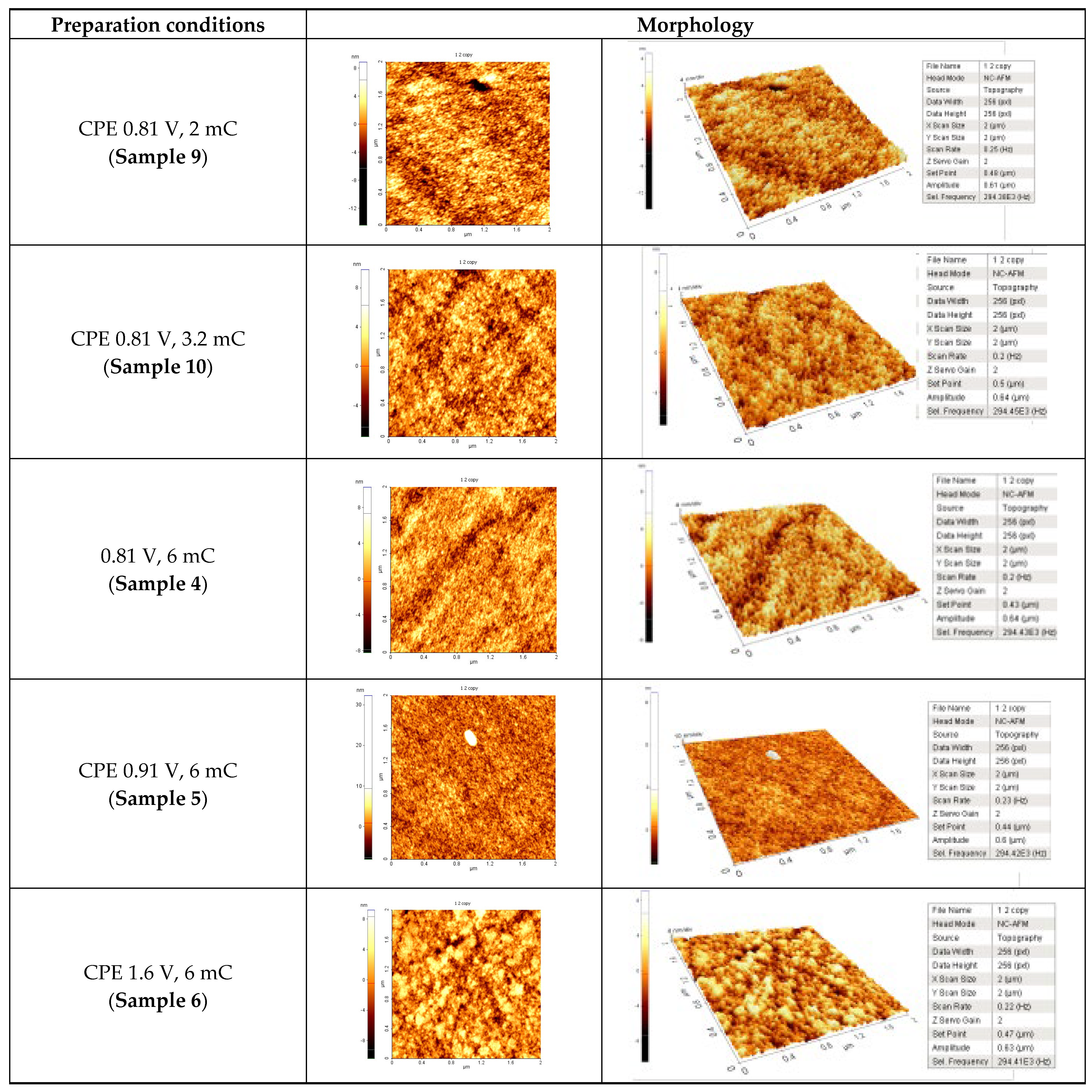
AFM tests were performed for the samples obtained by CPE. Figure 2a,b present the 2D and 3D images for Sample 5 obtained at a large scale (nm/div = 200), putting into evidence scattered granules. Figure 3 presents the 2D and 3D images for other samples investigated by AFM for 2 × 2 μm2. The AFM images contain topographic data. The height scale corresponds to a colour scale that differs from one image to another. The darkest colour is to the lowest point (zero height) and the lightest colour is to the highest point for each image.
In order to obtain information regarding the roughness, the root mean square (RMS) roughness was investigated on large areas of 40 × 40 μm2. More details were observed on smaller areas (2 × 2 μm2). For instance, Sample 9 is characterized by a very smooth surface with a roughness of 2.4 nm. Only a few grains with sizes 200–400 nm are present on the surface. The AFM image of the surface on 2 × 2 μm2 shows the nanostructured aspect with grains smaller than 50 nm and rare pores with diameters below 100 nm. Sample 10 has a smooth surface with roughness around 5.2 nm. Rare big grains with sizes of 600 nm −1 µm are scattered on the surface. These are formed from nanoparticles (NPs) with diameters below 100 nm. In addition, small pores (size smaller than 100 nm) are noticed. Sample 4 has a surface with low roughness (4.2 nm); the presence of small grains is observed on 2 × 2 μm2. In addition, the appearance of very small pores is noticed. Some of these grains with sizes below 70 nm are agglomerated together into big islands, sized 1.3–2 µm. The maximum height of these islands is around 150 nm. Sample 5 presents a very rough surface, with a roughness value of 35.8 nm due to the presence of big grains with sizes around 1 µm. These scattered grains seem to be formed by the aggregation of NPs with sizes between 200–500 nm. Sample 6 shows a very smooth surface with roughness around 3 nm; investigated on a small area, pores with diameter below 100 nm are noticed.
The ordering of the AFM samples (Table 3 and Figure 3) followed the possibility of comparing the influence of electropolymerization charge (Samples 9, 10, and 4) and potential (Samples 4–6) on the RMS for the studied CMEs.

3.4. FTIR Results

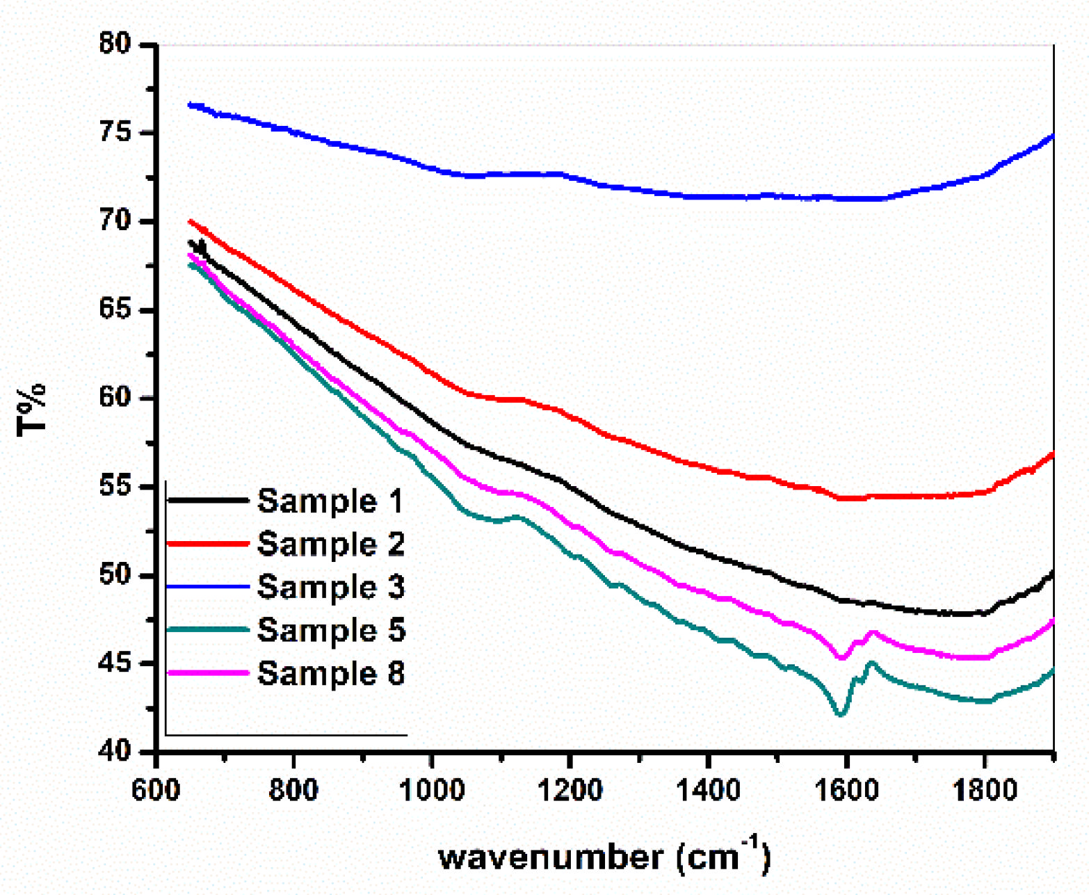
FTIR spectra (given in Figure 4) were recorded for the samples obtained by scanning (Samples 1–3) and CPE (Samples 5, 8) according to Table 1, and the specific wave numbers for Samples 5 and 8 were collected from Figure S3. Transmission minima have been detected only for the samples prepared by CPE, as follows:
Sample 5: 1793 cm−1, 1590 cm−1, 1625 cm−1;
Sample 8: 1775 cm−1, 1595 cm−1, 1625 cm−1.
The peaks 1775 cm−1 and 1793 cm−1 were attributed to the specific vibration of thiophene. The peaks 1590 cm−1 and 1625 cm−1 could be due to the overlapping of the specific vibration of thiophene pyridine.

3.5. Fluorescence Studies

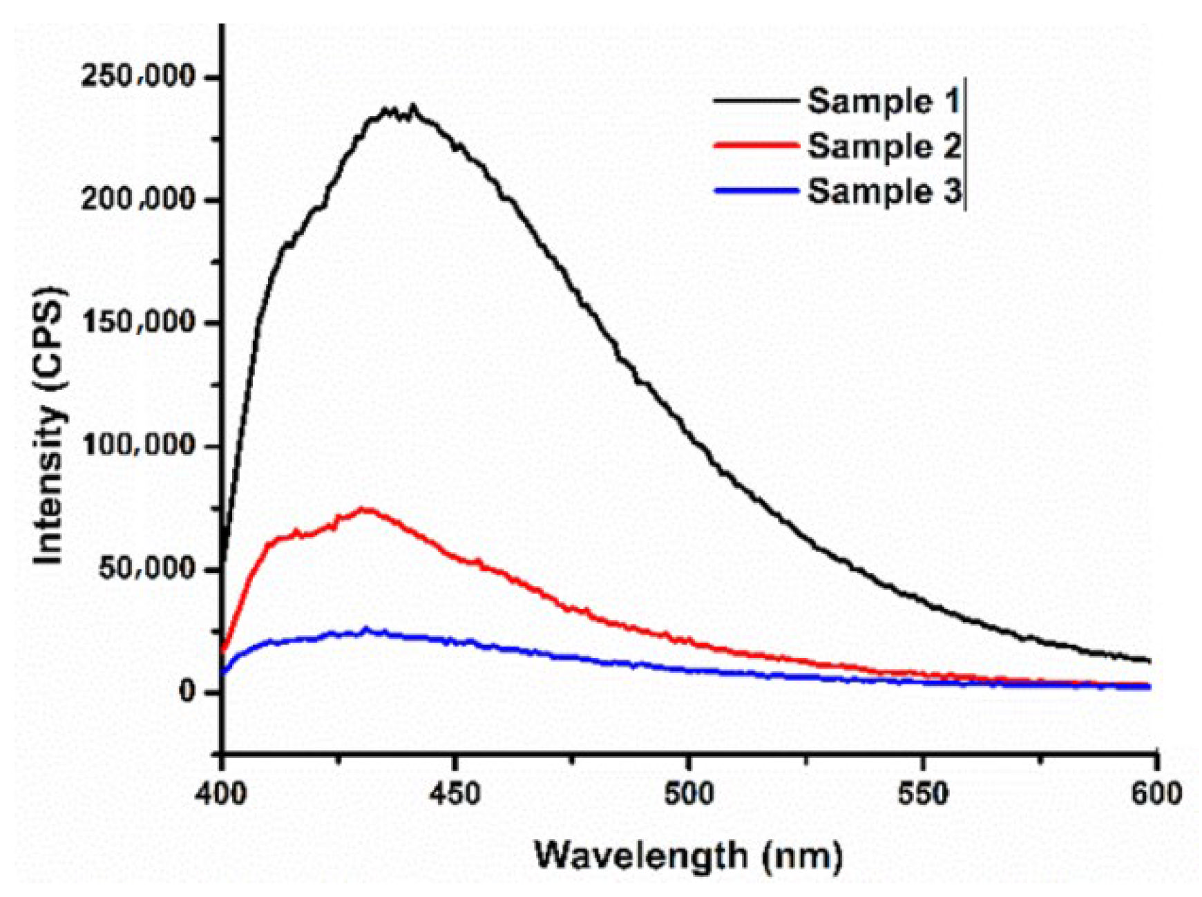
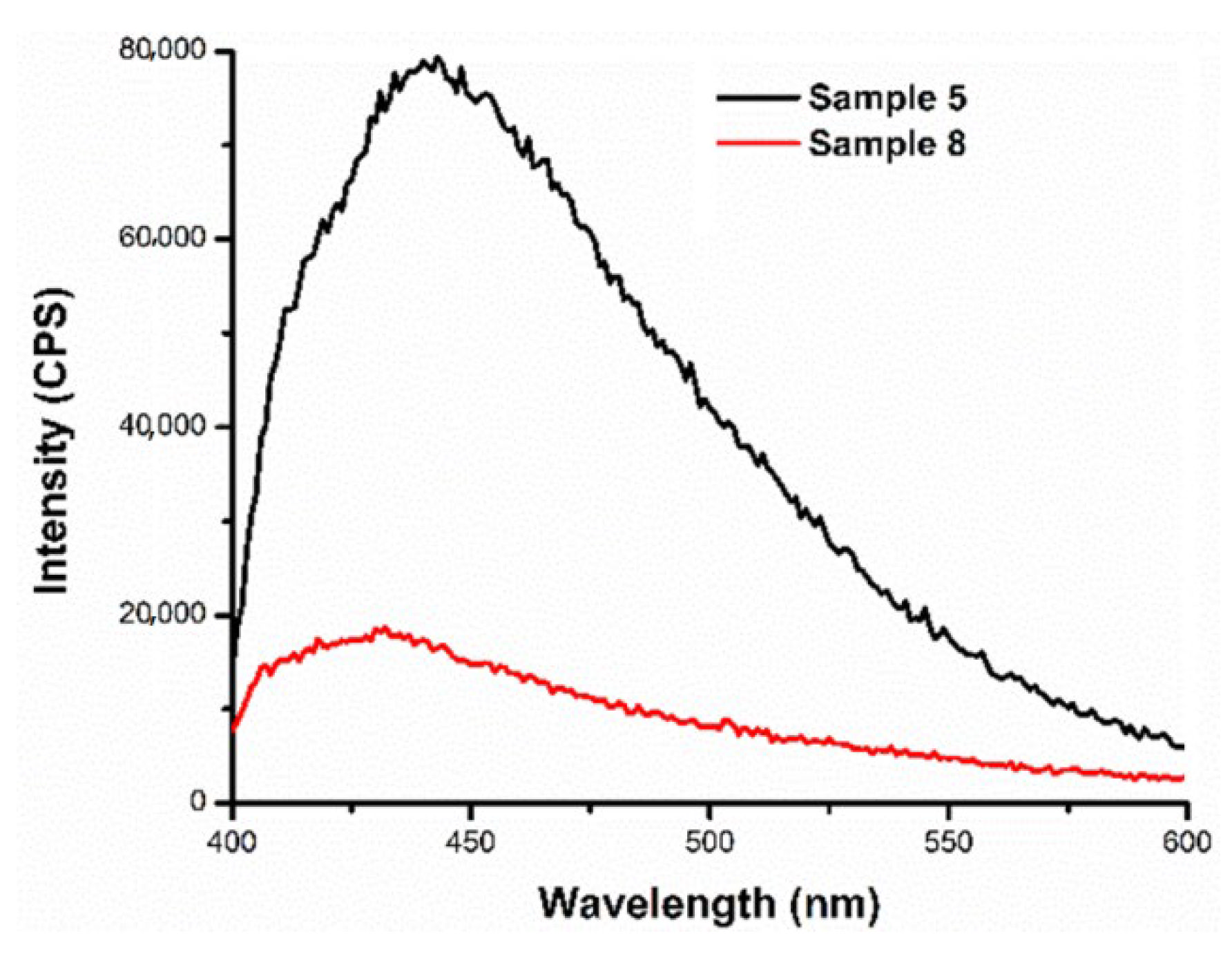
Fluorescence spectra were recorded for the samples obtained by scanning (Figure 5) and CPE (Figure 6), and the main characteristics wavelength of the maximum fluorescence (λmax), intensity, and full width half maximum (FWHM) are collected in Table 4.

3.6. Electrochemical Evidence for Film Formation

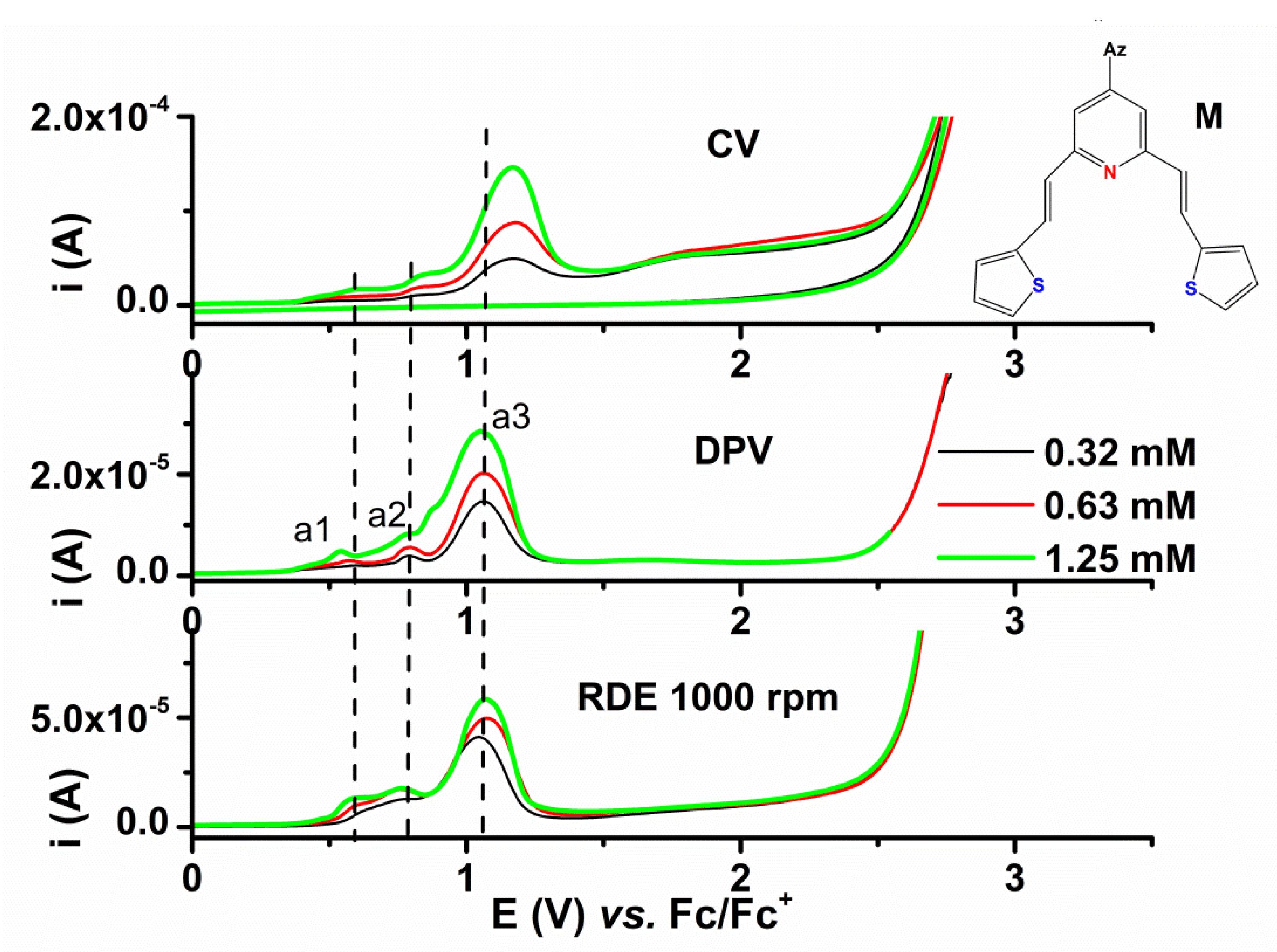
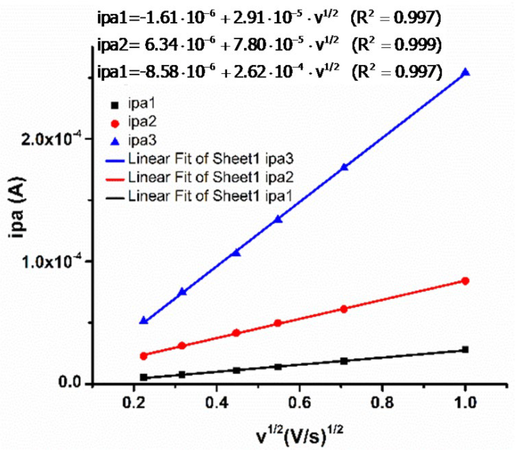
The electrochemical studies of the monomer M containing complexing (thiophen-2-yl)vinyl symmetrically substituted pyridine fragments (Figure 7) were performed by CV, DPV, and RDE to confirm the formation of films, which are coloured as mentioned in Table 1. This anodic polymerization can be explained considering the three anodic processes which have the peaks denoted a1–a3 (Figure 7). These peaks were attributed to the monomer oxidation processes, as previously demonstrated [19]. All processes are irreversible. The CV curves obtained at variable scan rates show the current peaks’ increase with the scan rate (Figure 8). Linear dependences of the peak currents on the square root of the scan rate were found, with different slopes for a1–a3, as shown in Figure 9.
More evidence on the film formation was obtained during the preparation of films by scanning. Figure S4 shows the successive CV curves up to 0.8 V where the first cycle is different from the following ones, which are shifted to more positive potentials. After a decrease between cycle 1 and cycle 2, peak currents increase with cycling. Figure S5, obtained on wider potential domains (beyond peak a3), shows a sudden and continuous decrease in the currents in the successive cycles.

4. Discussion

The electrochemical studies by CV, DPV, and RDE of the monomer confirmed the formation of films as a result of the three anodic processes which have the peaks denoted a1–a3. As Figure 7 shows, the increase in the a3 peak current with concentration is more evident for CV and DPV than for RDE curves. This is correlated with the formation of insulating films corresponding to more positive potentials (at the peak a3), which leads to the clear decrease in the current during successive scanning, as shown in Figure S5. Both DPV and RDE methods were applied at the same scan rate, but in the RDE method the supply of monomer to the electrode surface is higher due to the electrode rotation. This leads to the faster coating of the electrode with insulating film and, consequently, the decrease in the current at the potential of the a3 peak appears more evident in the case of RDE than the DPV method.
However, the different behaviour in the case of RDE vs. CV or DPV does not occur at the potential of the peak a1, where the recorded RDE currents similarly increase with concentration (Figure 7). A more in-depth study of the CV curves during the preparation of the electrode by scanning shows that the polymerization process also takes place at the a1 potential (Figure S4). In this figure, cycle 1 is shown with a bold black line, and the following cycles are shown with red thin lines with the corresponding number of the cycle. For the a1peak, some characteristics specific to the formation of films were observed: the irreversibility of the peak, the displacement of the peak potential in the second cycle towards more positive values than in the 1st cycle, the appearance of a new redox couple around the potential of 0.3 V specific for the reversible process of polymer oxidation/ reduction, and the increase in the current peaks for this couple with the number of cycles. According to Figure 7 and Figure S4, the polymerization occurs at a1 peak potential, but it takes place in a different way than at the a3 peak potential, leading to a conductive film. The new redox couple is due to the oxidation/ reduction of the polymer formed by scanning with the anodic limit of 0.8 V. Through cycling, the current increases as the number of cycle progresses. These facts allow highlighting the two possible ways of electropolymerization at a1 and a3 peak potentials. At more positive potentials than that of the a3 peak, the current drops suddenly for all methods, indicating the coverage with non-conductive films.
The CV curves obtained at variable scan rates (Figure 7) show that all processes are irreversible in all domains. The current peak slopes for a1 and a3 given in Figure 9 are very different and increase significantly from a1peak to a3 peak, a fact which can be explained by assuming that different films are formed if the electropolymerization is performed at a1 and a3 peak potentials.
Based on the voltammetric methods which highlight the film formation, the values of the potentials favourable to the formation of the films (between 0.8 V and 1 V) were established. The surfaces of the films obtained at these significant potentials were further analysed as morphology, roughness, and fluorescence.
Investigation and morphological characterization of the modified electrodes based on M performed using SEM, EDX, AFM, FTIR, and fluorescence methods indicated that coloured films obtained either by scanning or by CPE (Table 1) also have different properties.
SEM analysis for films formed by scanning shows that the films obtained at lower limits of anodic scans (lower than 0.81 V) are unstructured, while those at higher limits of anodic scans are structured. The film obtained by scanning to 0.91 V revealed a nanometric structure with 3–11 nm size. The film obtained by scanning to 1.6 V also revealed a nanometric structure with 8.5–22 nm size (Figure S2). When prepared by CPE, the films show uniform surfaces with rare nanoclusters. The thicker films (prepared with a charge of 6 mC) show higher dimensions (150–250 nm) of nanoclusters than those prepared with 3.2 mC (100–200 nm), both of them being obtained at the same potential of 0.91 V. However, thinner (3.2 mC) films prepared by CPE have more nanoclusters per unit area (in comparison with those prepared with 6 mC).
EDX for films formed by scanning do not highlight S or N, probably due to the limited thickness of the films. The films formed by CPE (usually thicker than those by scanning) reveal only the presence of S. This fact can be correlated with the presence of two S atoms in relation to 1 N atom in the chemical structure of the monomer. In addition, Cl and O were detected as well. Their presence is derived from ClO4 anion traces from the supporting electrolyte TBAP.
AFM topography showed the presence of columnar-shaped features on the surfaces (with a maximum height of 150 nm). The calculated RMS roughness values seen in Table 3 show the influence of charge and electropolymerization potential on RMS roughness for the studied CMEs. The surface roughness parameters of the layers deposited by CPE at the same potential of 0.81 V, but using different charges, are in the same range of values (2–6 mC), so the influence of the electropolymerization charge on the roughness is not major at this potential. The images of the layers prepared by CPE at constant charge (6 mC) but variable potentials indicate that at the intermediate potential of 0.91 V the surfaces with the highest roughness are obtained. This potential corresponds to the electropolymerization potential for which the better analytical signal for CMEs (prepared under the same conditions) used in the detection of HM ions in synthetic samples was reported. In this way, the surface roughness can be correlated with the analytical performances of the layers deposited by CPE [19]. This can be explained by the increase in the active surface by the presence of big grains with sizes around 1 µm, which seem to be formed by the aggregation of NPs with sizes between 200–500 nm.
FTIR spectra show that the organic films are thin, and the graphite substrate shields the vibrations of the bonds in the films. Transmission minima detected only on samples prepared by CPE are attributed to the presence of thiophene and duplication of specific binding thiophene or pyridine. It can be assumed that the electropolymerization is of the π-steaking type if the bands for thiophene are not affected. This proves that the symmetry of the complexing unit is maintained in the complexing polymer justifying also the good analytical ability of chemically modified electrodes based on M. This result is still under evaluation and systematic studies are to be carried out for validation.
Fluorescence spectra show that the samples prepared by scanning (Samples 1–3) have higher fluorescence intensity than those prepared by CPE (Samples 5 and 8). As the anodic limit of the scan increases, the fluorescence decreases. The fluorescence of thicker films prepared by CPE is higher. The full width at half maximum (FWHM) for azulene films shown in Table 4 indicates the samples present a broad emission band extended between 400–600 nm, with different peak positions. These results show that the polymerization by scanning preserves the fluorescence properties of the films, while that by CPE limits the film fluorescence. This conclusion is important for future optical applications of these films.
Electrochemical studies were carried out to confirm the reproducibility of the formed films. This is reflected in the following: (i) the CV curves (Figure S6) of the ligand obtained on the same electrode after a thorough cleaning of the glassy carbon electrode, (ii) the chronoamperograms (Figure S7) obtained at the same potential, but using different charges which have an identical evolution, (iii) the DPV stripping curves (Figure S8) obtained for different concentrations of target species (Pb) in the accumulation solution which have an error below 5%.

5. Conclusions

The differences between the polymerization potentials stand for differentiation of the formed films and their characteristics. The use of several methods (SEM, AFM, FTIR, and fluorescence) to investigate the surfaces of CMEs allowed the highlighting of several types of properties that confirm the formation of films and led the elaboration of decisions regarding the use of electrodes. The aspects related to the morphology were correlated with the electrochemical properties of the monomer to explain its mode of action when fixed on the surface. The surface characteristics are related to the detection capacity of the chemically modified electrode. As concerns the preparation methods of electrodes based on M, the study demonstrated that surfaces prepared by scanning are favourable for fluorescence applications, while those prepared by controlled potential electrolysis can be recommended for sensors preparation. The research is in progress, aiming to build a large basis on azulene compounds as monomers for CMEs and also for fluorescence applications.

Supplementary Materials

The following supporting information can be downloaded at: https://www.mdpi.com/article/10.3390/sym14122506/s1, Basic properties for M and characterization by elemental analysis, UV-Vis, IR, 1H NMR, 13C-NMR, and MS, Figure S1 a: EDX spectrum for Sample 5; Figure S1 b EDX spectrum for Sample 8; Figure S2: SEM image for Sample 3 with nanometric structures of 9.8 nm -22.6 nm (a) and 8.5 -19 nm (b); Figure S3. FTIR spectra and specific wave numbers for Samples 5 (blue) and 8 (red); Figure S4: CV curves during the preparation of CMEs by scanning in the potential range of the first anodic peak a1 (short anodic range potential); [M] = 0.63 mM; Figure S5. CV curves during the preparation of CMEs by scanning on larger anodic range of potential; [M] = 0.63 mM; Figure S6. CV curves (0.1 V/s) for [M] = 0.63 mM recorded successively on glassy carbon electrode (3 mm diameter). Figure S7. Chronoamperograms during CPE at 1.2 V (0.5 mC) in solution of [M]; Figure S8. Stripping DPV curves for CME prepared by CPE at 1.2V (0.5 mC) in a solution of [M].

Author Contributions

Conceptualization, I.C., E.-M.U. and R.I.; methodology, E.-M.U. and I.C.; software, E.D. and A.-M.P.; validation, I.C., C.V., E.D., R.I. and E.-M.U.; formal analysis, R.I. and E.-M.U.; investigation, I.C., A.-M.P., C.V., E.D., R.I. and E.-M.U.; resources, E.-M.U., I.C., C.V. and R.I.; data curation, R.I. and E.-M.U.; writing—original draft preparation, I.C., R.I. and E.-M.U.; writing—review and editing, E.-M.U., R.I. and I.C.; visualization, E.-M.U., R.I. and I.C.; supervision, E.-M.U., I.C. and E.D.; project administration, E.-M.U., R.I. and I.C.; funding acquisition, E.-M.U. All authors have read and agreed to the published version of the manuscript.

Funding

This research received no external funding.

Data Availability Statement

Not applicable.

Acknowledgments

This work was supported by the Romanian Ministry of Research, Innovation and Digitalization (MRID), Core Program PN 18N/2019, and by the MRID through Program I—Development of the National R & D System, Subprogram 1.2—Institutional Performance Projects for Excellence Financing in RDI, contract no. 18PFE/2021, project ID PN-II-PT-PCCA-2013-4-2151, contract number 236/2014.

Conflicts of Interest

The authors declare no conflict of interest.

References

  1. Shoji, T.; Yokoyama, R.; Ito, S.; Watanabe, M.; Toyota, K.; Yasunamid, M.; Morita, N. Synthesis of heteroarylazulenes: Transition metal free coupling strategy of azulene with heterocycles. Tetrahedron Lett. 2007, 48, 1099–1103. [Google Scholar] [CrossRef]
  2. Shoji, T.; Ito, S. The Preparation and Properties of Heteroarylazulenes and Hetero-Fused Azulenes. Adv. Heterocycl. Chem. 2018, 126, 1–54. [Google Scholar]
  3. Răzuș, A.C.; Bîrzan, L. Synthesis of azulenic compounds substituted in the 1-position with heterocycles. Mon. Chem. 2019, 150, 139–161. [Google Scholar] [CrossRef]
  4. Shoji, T.; Okujima, T.; Ito, S. Development of Heterocycle-Substituted and Fused Azulenes in the Last Decade (2010–2020). Int. J. Mol. Sci. 2020, 21, 7087. [Google Scholar] [CrossRef]
  5. Răzuș, A.C. Azulene Moiety as Electron Reservoir in Positive Charged Systems; Short Survey. Symmetry 2021, 13, 526. [Google Scholar] [CrossRef]
  6. Shoji, T.; Yamazaki, A.; Katoh, R.; Shimamura, K.; Sakai, R.; Yasunami, M.; Okujima, T.; Ito, S. Synthesis, Reactivity, and Properties of Benz[a] azulenes via the [8+2] Cycloaddition of 2H-Cyclohepta[b]furan-2-ones with an Enamine. J. Org. Chem. 2022, 87, 5827–5845. [Google Scholar] [CrossRef]
  7. Ou, L.; Zhou, Y.; Wu, B.; Zhu, L. The unusual physicochemical properties of azulene and azulene-based compounds. Chin. Chem. Lett. 2019, 30, 1903–1907. [Google Scholar] [CrossRef]
  8. Buică, G.-O.; Bîrzan, L.; Popescu (Mandoc), L.-R.; Ivanov, A.A.; Ungureanu, E.-M. Thermodynamics of interactions between lead(II) and cadmium(II) ions and azulene-based complexing polymer films. J. Solid State Electrochem. 2016, 20, 401–411. [Google Scholar] [CrossRef]
  9. Heitzmann, M.; Bucher, C.; Moutet, J.-C.; Pereira, E.; Rivas, B.L.; Royal, G.; Saint-Aman, E. Characterization of metal cations-complexing polymer films interactions followed with anodic stripping voltammetry. J. Electroanal. Chem. 2007, 610, 147–153. [Google Scholar] [CrossRef]
  10. Heitzmann, M.; Bucher, C.; Moutet, J.-C.; Pereira, E.; Rivas, B.L.; Royal, G.; Saint-Aman, E. Complexation of poly(pyrrole-EDTA like) film modified electrodes: Application to metal cations electroanalysis. Electrochim. Acta 2007, 52, 3082–3087. [Google Scholar] [CrossRef]
  11. Buică, G.-O.; Lazăr, I.-G.; Saint-Aman, E.; Tecuceanu, V.; Dumitriu, C.; Ivanov, A.A.; Stoian, A.B.; Ungureanu, E.-M. Ultrasensitive modified electrode based on poly (1 H-pyrrole-1-hexanoic acid) for Pb (II) detection. Sens. Actuators B: Chem. 2017, 246, 434–443. [Google Scholar] [CrossRef]
  12. Gutierrez, A.G.P.; Gutierrez, S.; Ordaz, A.A.; Griveau, S.; Zagal, J.H.; Bedioui, F. Preparation and Characterization of Modified Electrodes Based on Carbon Nanotubes/Pyrrole/Cobalt Phthalocyanine for the Development of Hybrid Materials for the Electrochemical Activation of 2-mercaptoethanol. ECS Trans. 2008, 15, 133–141. [Google Scholar] [CrossRef]
  13. Wajs, E.; Fernández, N.; Fragoso, A. Supramolecular biosensors based on electropolymerised pyrrole–cyclodextrin modified surfaces for antibody detection. Analyst 2016, 141, 3274–3279. [Google Scholar] [CrossRef] [PubMed] [Green Version]
  14. Oliveira, R.D.; Santos, C.S.; Garcia, J.R.; Vidotti, M.; Marchesi, L.F.; Pessoa, C.A. IR drop studies of poly(aniline)-based modified electrodes. J. Electroanal. Chem. 2020, 878, 114662. [Google Scholar] [CrossRef]
  15. Lete, C.; Lupu, S.; Marin, M.; Badea, M. New composite materials used in the phenol electroanalysis. Part I. poly(azulene)/Prussian blue and Prussian blue/poly(azulene) films. Rev. Roum. Chim. 2010, 55, 335–340. [Google Scholar]
  16. Buică, G.-O.; Ungureanu, E.-M.; Bîrzan, L.; Răzuș, A.C.; Mandoc, L.-R. Voltammetric sensing of lead and cadmium using poly(4-azulen-1-yl-2,6-bis (2-thienyl)pyridine) complexing films. J. Electroanal. Chem. 2013, 693, 67–72. [Google Scholar] [CrossRef]
  17. Lazăr, I.-G.; Diacu, E.; Ungureanu, E.-M.; Buică, G.-O.; Bîrzan, L.; Arnold, G.-L. Modified electrodes based 2,6-bis((E)-2-(thiophen-2-yl)-4-(4,6,8-trimethylazulen-1-yl)pyridine for heavy metals sensing. UPB Sci. Bull. Ser. B 2017, 79, 23–26. [Google Scholar]
  18. Oprișanu, A.; Lazăr, I.-G.; Pop, M.D.; Ungureanu, E.-M.; Isopescu, R.; Bîrzan, L. Polyazulene Based Materials For Heavy Metal Ions Detection. IOP Conf. Ser. Mater. Sci. Eng. 2017, 68, 2215–2218. [Google Scholar]
  19. Brotea, A.-G.; Matica, O.-T.; Musina (Borsaru), C.E.; Ungureanu, E.-M. Advanced materials based on 4-(azulen-1-yl)-2,6-bis((E)-2-(thiophen-2-yl)vinyl)pyridine. UPB Sci. Bull. Ser. B 2022, 84, 53–62. [Google Scholar]
  20. Ciocîrlan, O.; Ungureanu, E.-M.; Vasile (Corbei), A.-A.; Ștefaniu, A. Properties Assessment by Quantum Mechanical Calculations for Azulenes Substituted with Thiophen-or Furan-Vinyl-Pyridine. Symmetry 2022, 14, 354. [Google Scholar] [CrossRef]
  21. Wang, B.-C.; Lin, Y.-S.; Chang, H.; Wang, P.-Y. Theoretical studies of azulene and its derivatives. Can. J. Chem. 2000, 78, 224–232. [Google Scholar] [CrossRef]
  22. Korichi, H.; Zouchoune, F.; Zendaoui, S.-M.; Zouchoune, B.; Saillard, J.-Y. The Coordination Chemistry of Azulene: A Comprehensive DFT Investigation. Organometallics 2010, 29, 1693–1706. [Google Scholar] [CrossRef]
  23. Mirzaei, M.S.; Taherpour, A.A.; Wentrup, C. Azulene–Naphthalene, Naphthalene–Naphthalene, and Azulene–Azulene Rearrangements. J. Org. Chem. 2022, 87, 11503–11518. [Google Scholar] [CrossRef] [PubMed]
  24. Kreuter, F.; Tonner, R. Surface functionalization with nonalternant aromatic compounds: A computational study of azulene and naphthalene on Si(001). J. Phys. Condens. Matter 2021, 33, 444003. [Google Scholar] [CrossRef] [PubMed]
  25. Birzan, L.; Cristea, M.; Draghici, C.; Tecuceanu, V.; Hanganu, A.; Ungureanu, E.-M.; Razus, A.C. 4-(Azulen-1-yl) six-membered heteroaromatics substituted in 2- and 6- positions with 2-(2-furyl)vinyl, 2-(2-thienyl)vinyl or 2-(3-thienyl)vinyl moieties. Tetrahedron 2017, 73, 2488–2500. [Google Scholar] [CrossRef]
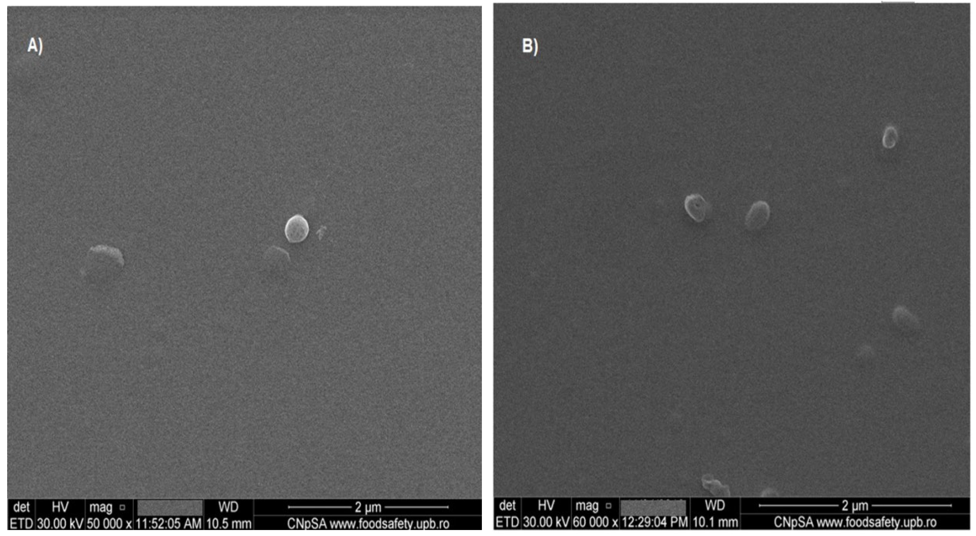
Figure 1. SEM images of the modified electrodes obtained by CPE at 0.91 V. The films were obtained using different polymerization charges: (A) 6 mC for Sample 5; (B) 3.2 mC for Sample 8.
Symmetry 14 02506 g001
Figure 2. AFM images for Sample 5: (a) 2D image for 40 × 40 μm2; (b) 3D image for 40 × 40 μm2.
Symmetry 14 02506 g002
Figure 3. AFM 2D—left side, and 3D—right side images for samples prepared in different conditions and investigated at a resolution of 2 × 2 μm2.
Symmetry 14 02506 g003
Figure 4. FTIR spectra for samples prepared by scanning (Samples 1–3) and CPE (Samples 5 and 8).
Symmetry 14 02506 g004
Figure 5. Fluorescence curves for the samples obtained by scanning according to Table 1.
Symmetry 14 02506 g005
Figure 6. Fluorescence curves for Samples 5 and 8 obtained by CPE according to Table 1.
Symmetry 14 02506 g006
Figure 7. CV, DPV, and RDE curves for M (Az stands for azulen-1-yl) at different concentrations (mM) in 0.1 M TPAP, CH3CN when scanning in the anodic range.
Symmetry 14 02506 g007
Figure 8. CV curves for M (1 mM) when scanning within the anodic scan range potentials of a1 (a) and a1–a3 (b) peaks.
Symmetry 14 02506 g008
Figure 9. Dependence of the peak currents on the square root of the scan rate; [M] = 1 mM in 0.1 M TBAP, CH3CN.
Symmetry 14 02506 g009
Table 1. CME sample preparation conditions and colour of the obtained films.
SampleFilm FormationFilm Colour
1Scanning 0.81 V 15 scansBlue
2Scanning 0.91 V 15 scansTurquoise
3Scanning 1.6 V 10 scansBrown
4CPE 0.81 V 6 mCEmerald green
5CPE 0.91 V 6 mCBlue
6CPE 1.6 V 6 mCGray
7CPE 0.91 V 2 mCDark turquoise
8CPE 0.91 V 3.2 mCGreenish yellow
9CPE 0.81 V 2 mCNavy blue
10CPE 0.81 V 3.2 mCYellow-green
Table 2. Morphology of the deposited films, obtained by scanning and CPE in different electropolymerization conditions.
SampleFilm Formation ParametersSEM and EDX Characteristics
1Scanning 0.81 V; 15 cyclesUnstructured organic film. EDX does not highlight either S or N.
2Scanning 0.91 V; 15 cyclesNanometric structure, size 3–11 nm. EDX does not highlight either S or N.
3Scanning 1.6 V; 10 cyclesNanometric structure, size 8.5–22 nm (Figure S2). Structured organic film. EDX does not highlight either S or N.
5CPE 0.91 V; 6 mCUniform film with rare nanoclusters (150–250 nm) (Figure 1a). EDX reveals the presence of S, O, and Cl.
8CPE 0.91 V; 3.2 mCUniform film with nanoclusters (100–200 nm) (Figure 1b). EDX reveals the presence of S, O, and Cl.
Table 3. RMS results from AFM data for the investigated samples.
SampleFilm Formation ParametersRMS at 40 × 40 μm2RMS at 2 × 2 μm2
9CPE 0.81 V; 2 mC2.42.0
10CPE 0.81 V; 3.2 mC5.22.0
4CPE 0.81 V; 6 mC4.22.4
5CPE 0.91 V; 6 mC35.82.2
6CPE 1.6 V; 6 mC2.92.5
Table 4. The main fluorescence characteristics of the discussed samples.
SampleRemarksλmax (nm)Intensity (cps)FWHM (nm)
1- thin film with nanometric particles with homogeneous dimensional distribution
- wavelength = 403–491 nm
438238,00080
2- thin film with nanometric particles with homogeneous dimensional distribution
- wavelength = 402–488 nm
43075,00060
3- thin film with nanometric particles with homogeneous dimensional distribution
- wavelength = 402–483 nm
43026,00070
5- thin film with nanometric particles with homogeneous dimensional distribution
- wavelength = 401–477 nm
44280,00080
8- thin film with nanometric particles with a wide range of dimensions
- wavelength = 408–522 nm
43119,00075
Publisher’s Note: MDPI stays neutral with regard to jurisdictional claims in published maps and institutional affiliations.