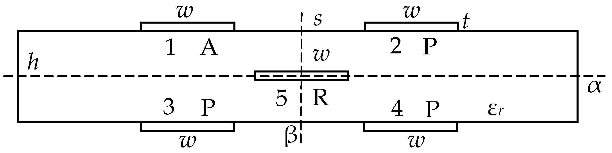
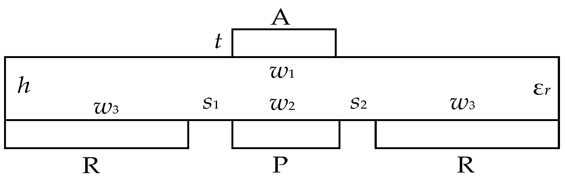
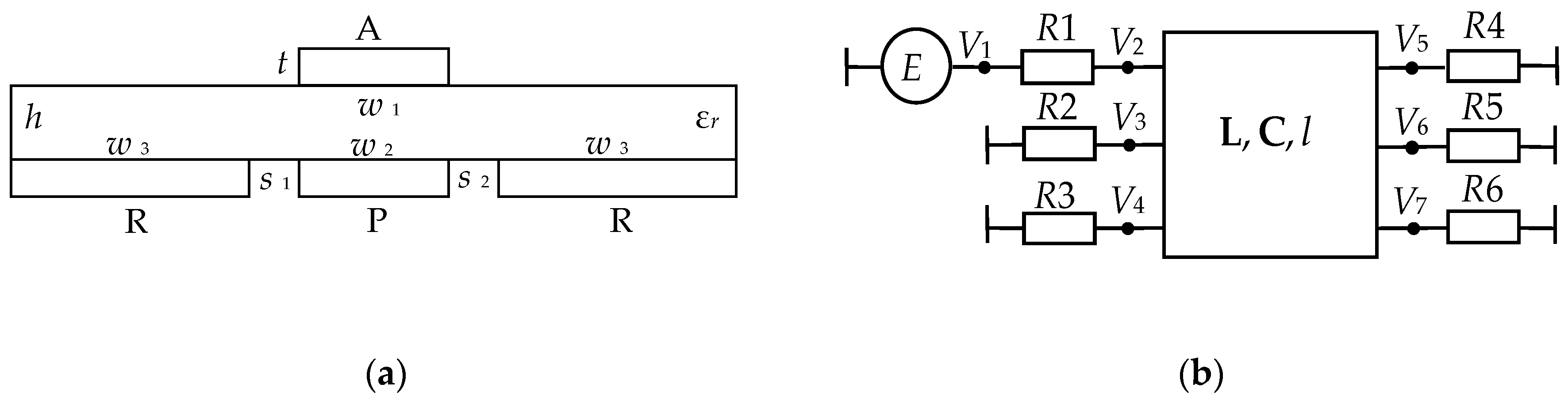
Figure 1.
Cross-section of the reflection-symmetric modal filters (MF). Conductors: A—active, P—passive, R—reference.
Figure 1.
Cross-section of the reflection-symmetric modal filters (MF). Conductors: A—active, P—passive, R—reference.
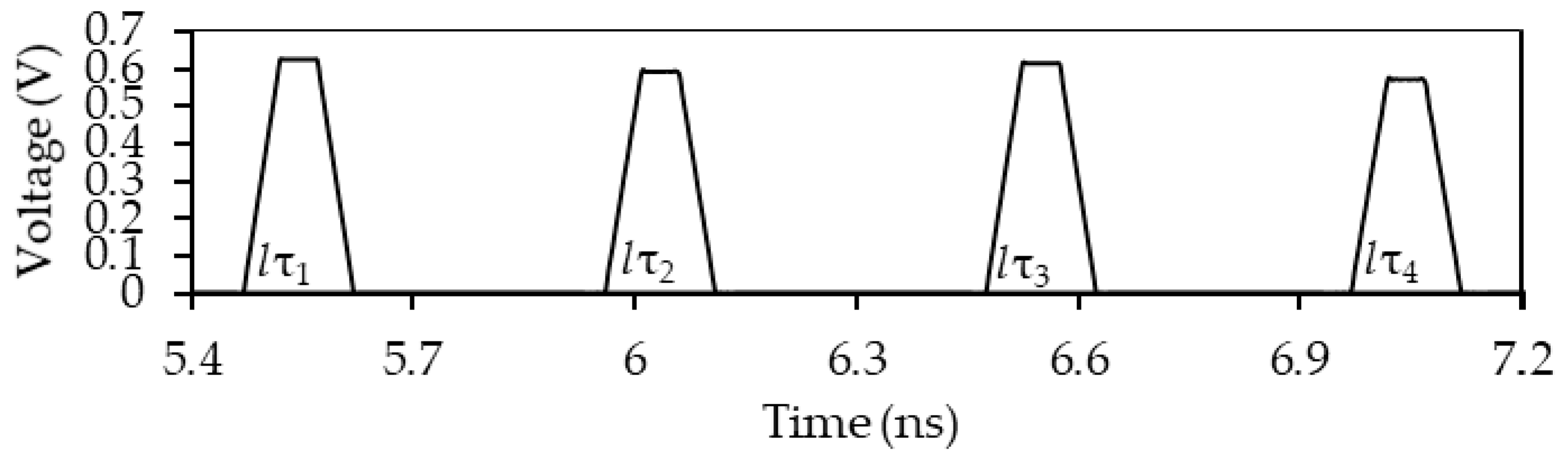
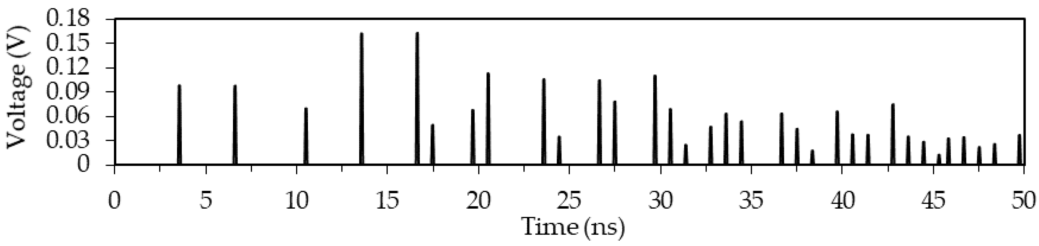
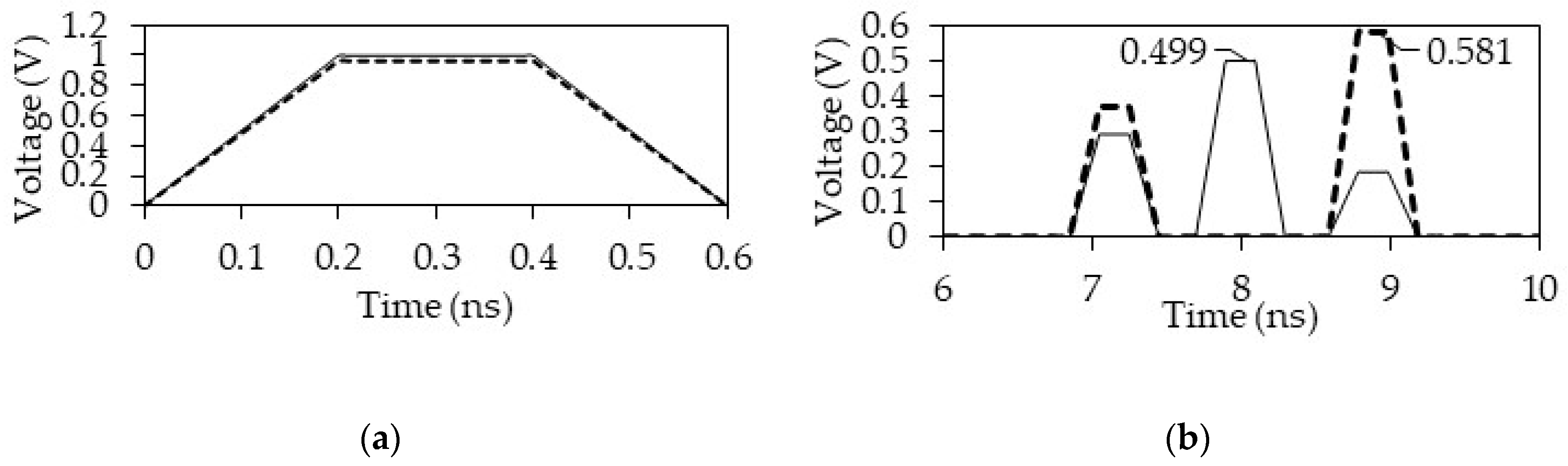
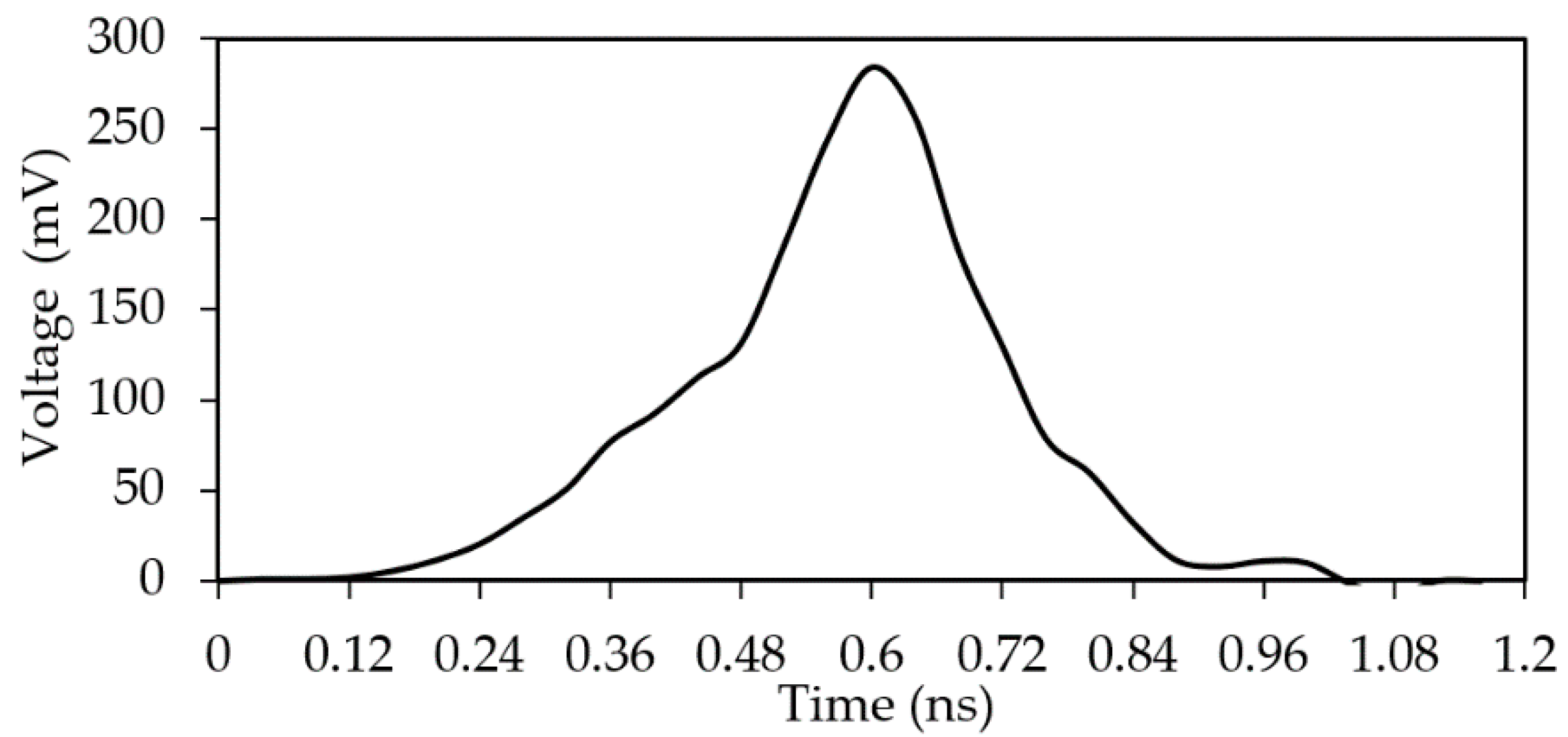
Figure 2.
Voltage waveform at the output of the reflection-symmetric MF excited by a single pulse with an electromotive force (EMF) of 5 V.
Figure 2.
Voltage waveform at the output of the reflection-symmetric MF excited by a single pulse with an electromotive force (EMF) of 5 V.
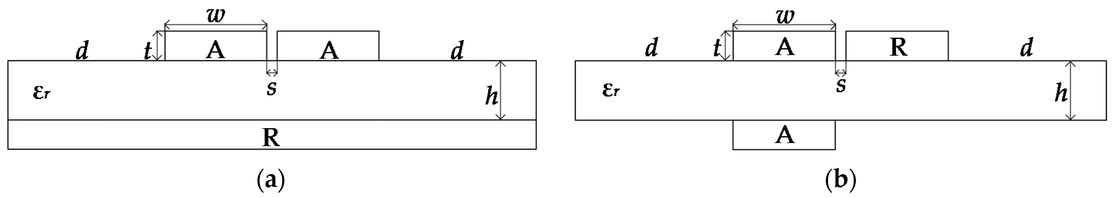
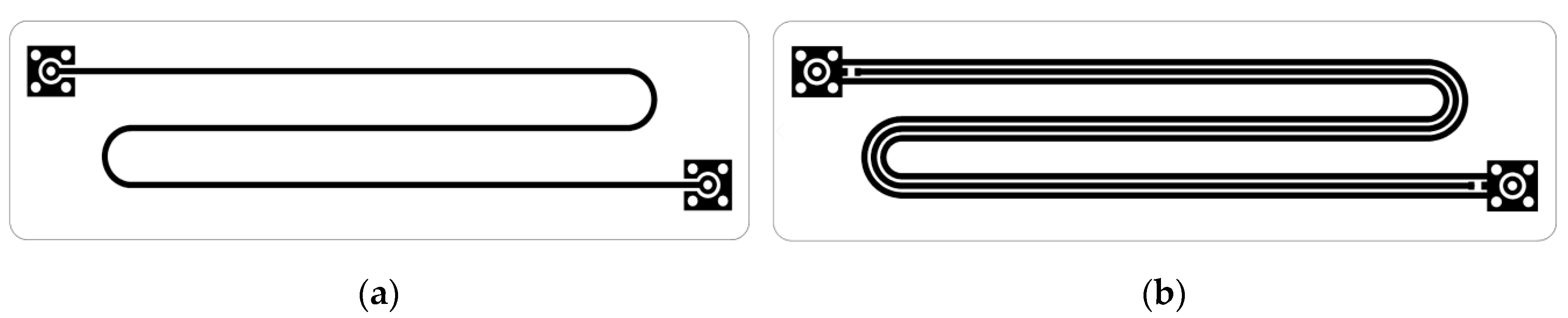
Figure 3.
Meander lines (ML) cross-sections: (a) based on the microstrip structure and (b) with broad-side coupling.
Figure 3.
Meander lines (ML) cross-sections: (a) based on the microstrip structure and (b) with broad-side coupling.
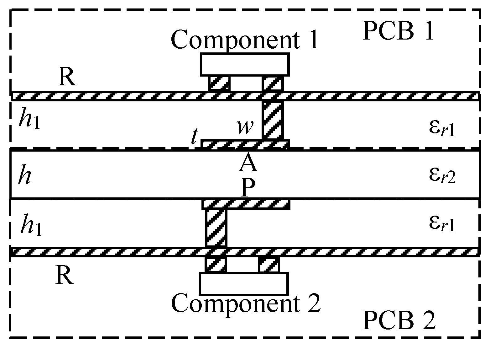
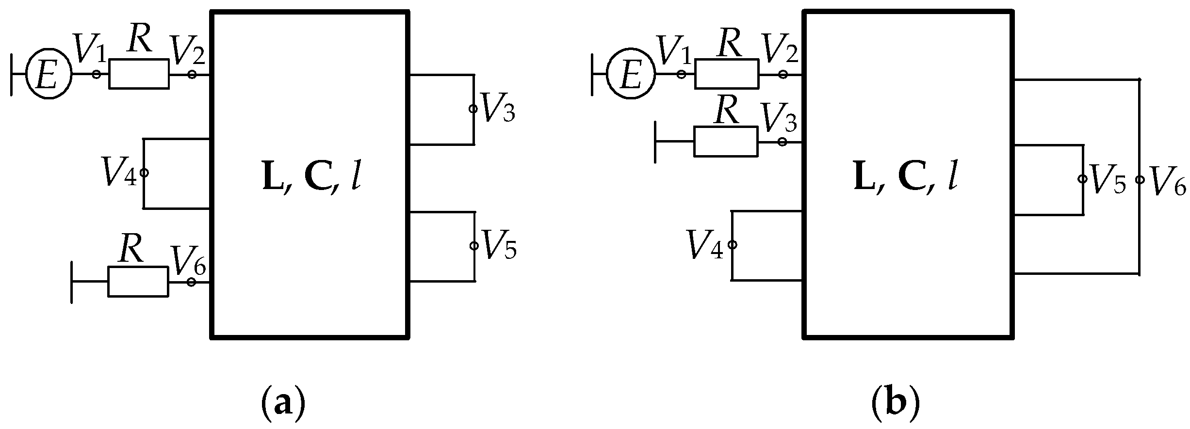
Figure 4.
Multilayer printed circuit board (PCB) configuration for the circuit with MR. Conductors: A—active, P—passive, R—reference.
Figure 4.
Multilayer printed circuit board (PCB) configuration for the circuit with MR. Conductors: A—active, P—passive, R—reference.
Figure 5.
Cross-section of the MF with a passive conductor in the reference plane cutout. Conductors: A—active, P—passive, R—reference.
Figure 5.
Cross-section of the MF with a passive conductor in the reference plane cutout. Conductors: A—active, P—passive, R—reference.
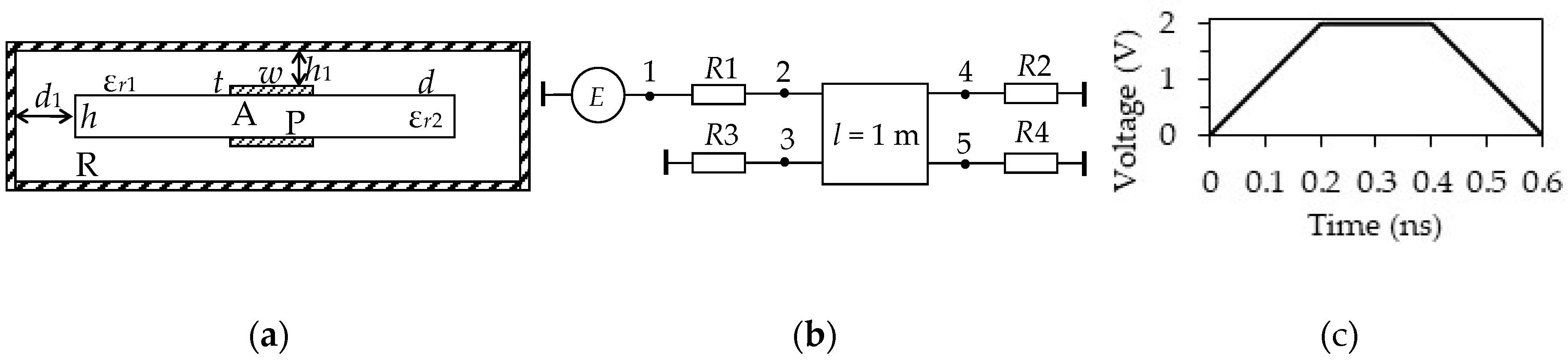
Figure 6.
(a) Cross-section and (b) equivalent circuit of the asymmetric MF.
Figure 6.
(a) Cross-section and (b) equivalent circuit of the asymmetric MF.
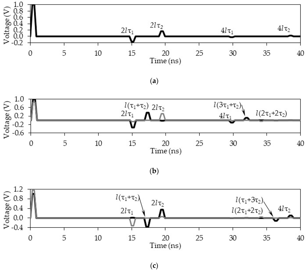
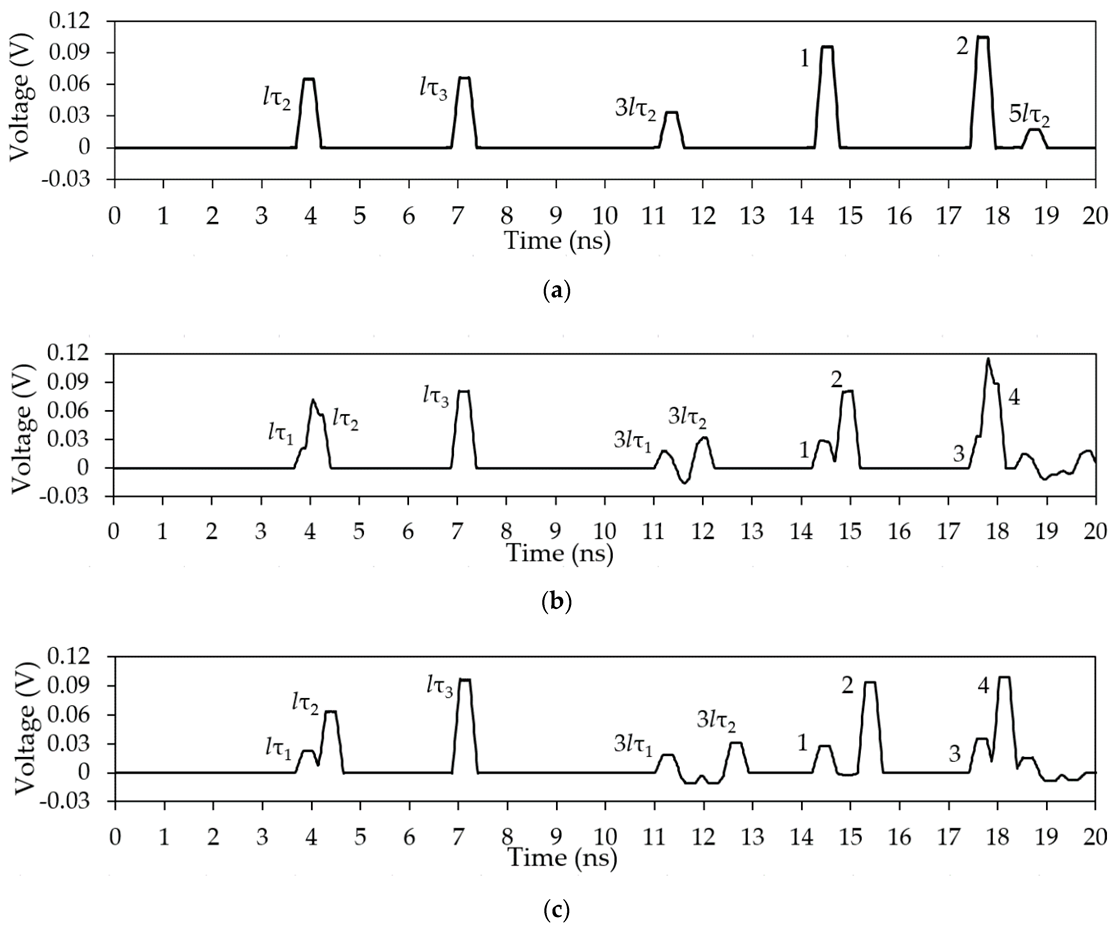
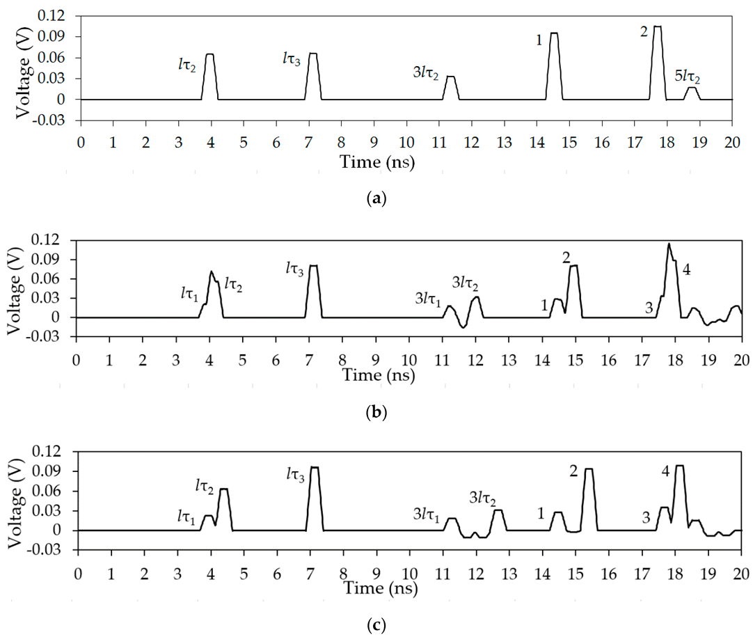
Figure 7.
Voltage waveform at the asymmetric MF output.
Figure 7.
Voltage waveform at the asymmetric MF output.
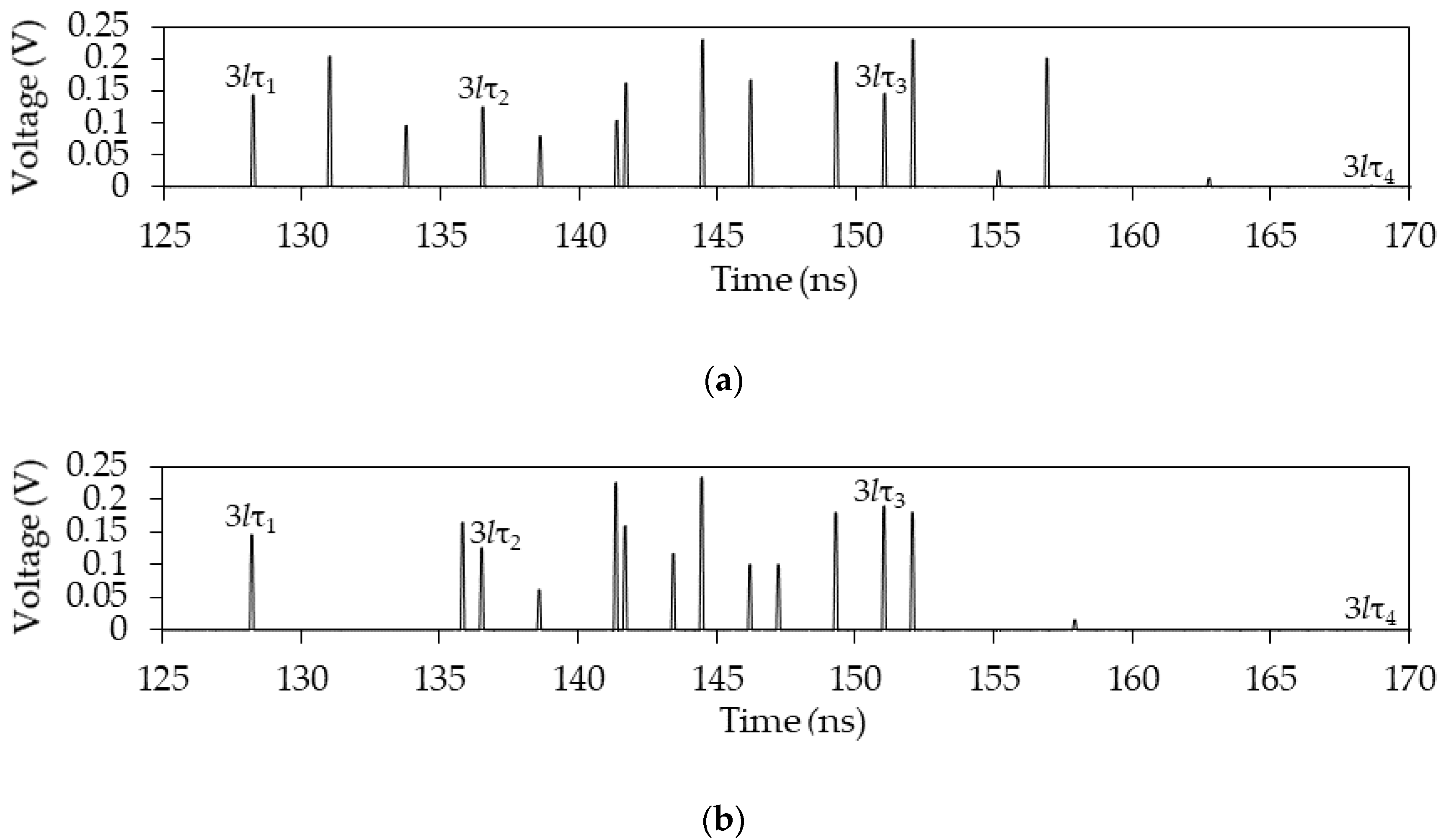
Figure 8.
(a) Circuit diagram and (b) output voltage waveform of ML with broad-side coupling.
Figure 8.
(a) Circuit diagram and (b) output voltage waveform of ML with broad-side coupling.
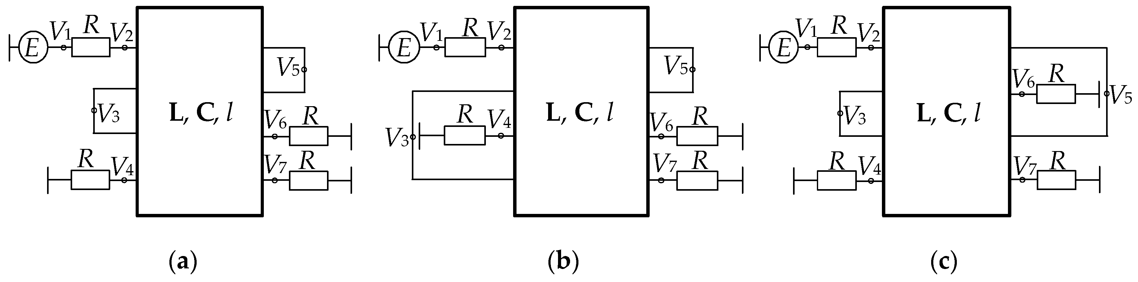
Figure 9.
Voltage waveform at the end of ML with broad-side coupling for (a) l = 80 mm and (b) l = 150 mm.
Figure 9.
Voltage waveform at the end of ML with broad-side coupling for (a) l = 80 mm and (b) l = 150 mm.
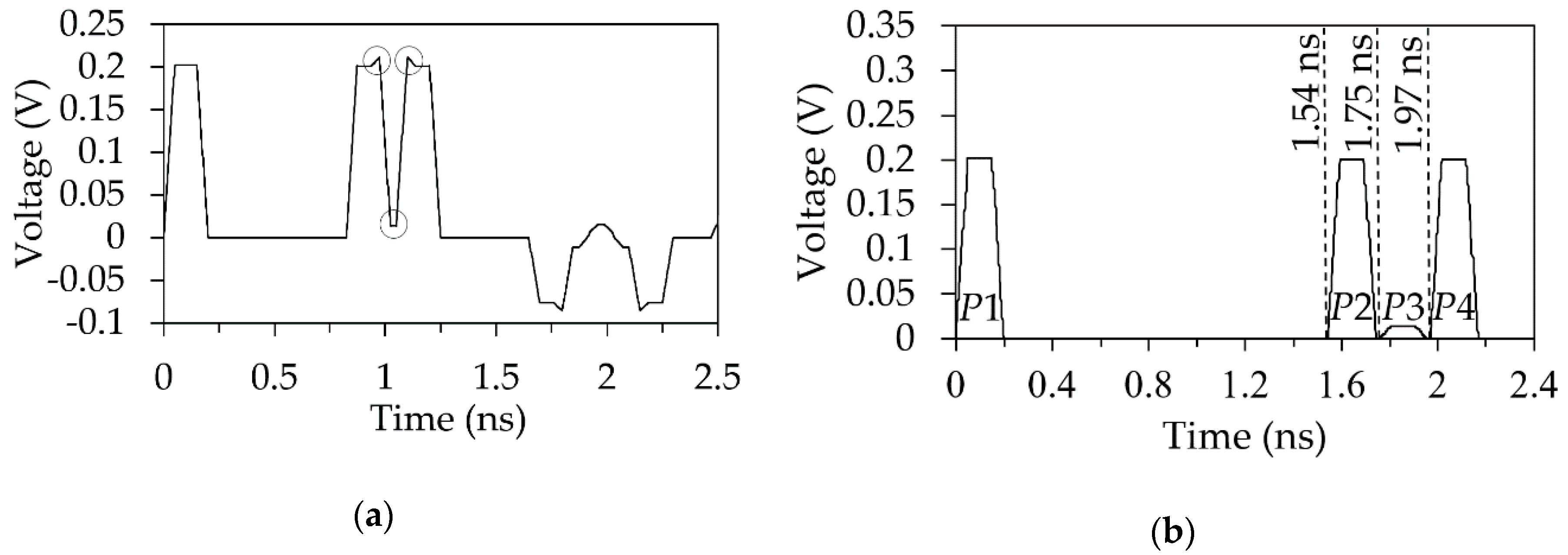
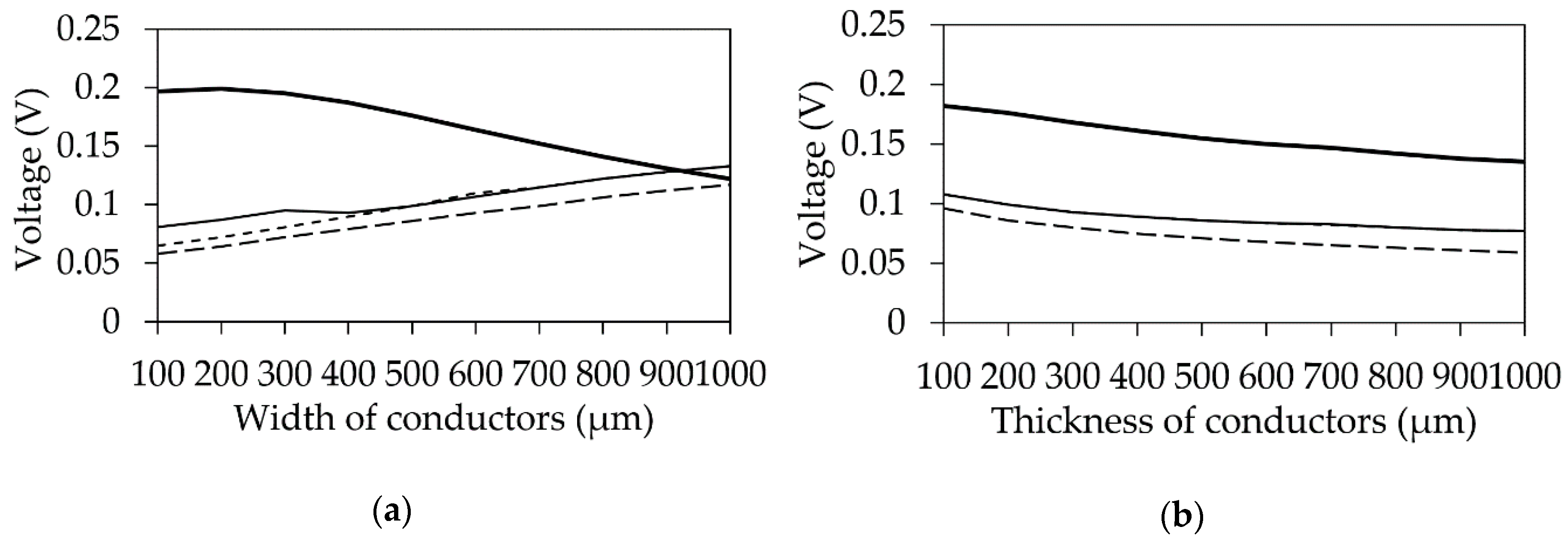
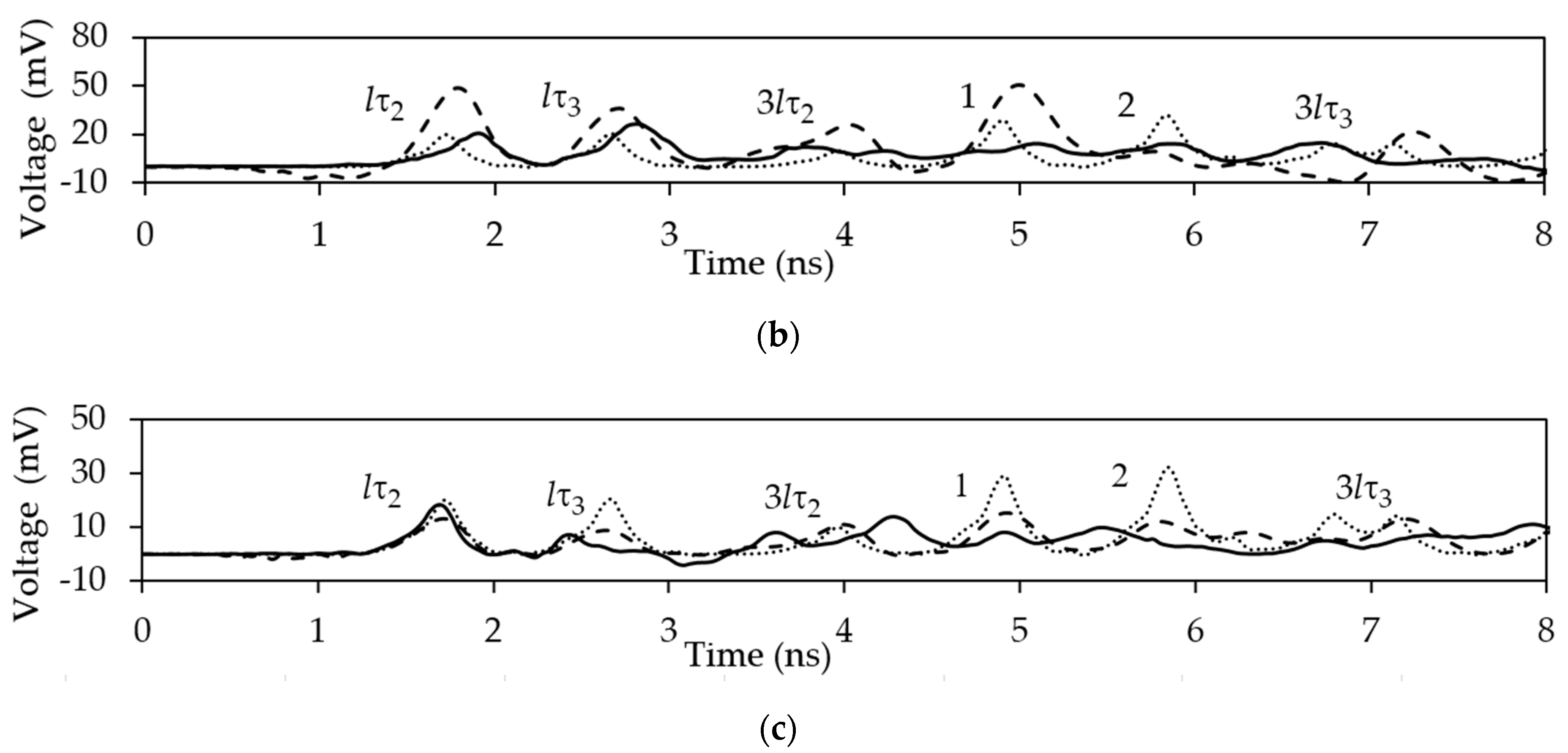
Figure 10.
Dependencies of P1 (– –), P2 (- -), P3 (––), and P4 (––) pulse amplitude at the end of asymmetrical ML on w (a), t (b), s (c), h (d), and εr (e) with the original unchanged parameters.
Figure 10.
Dependencies of P1 (– –), P2 (- -), P3 (––), and P4 (––) pulse amplitude at the end of asymmetrical ML on w (a), t (b), s (c), h (d), and εr (e) with the original unchanged parameters.
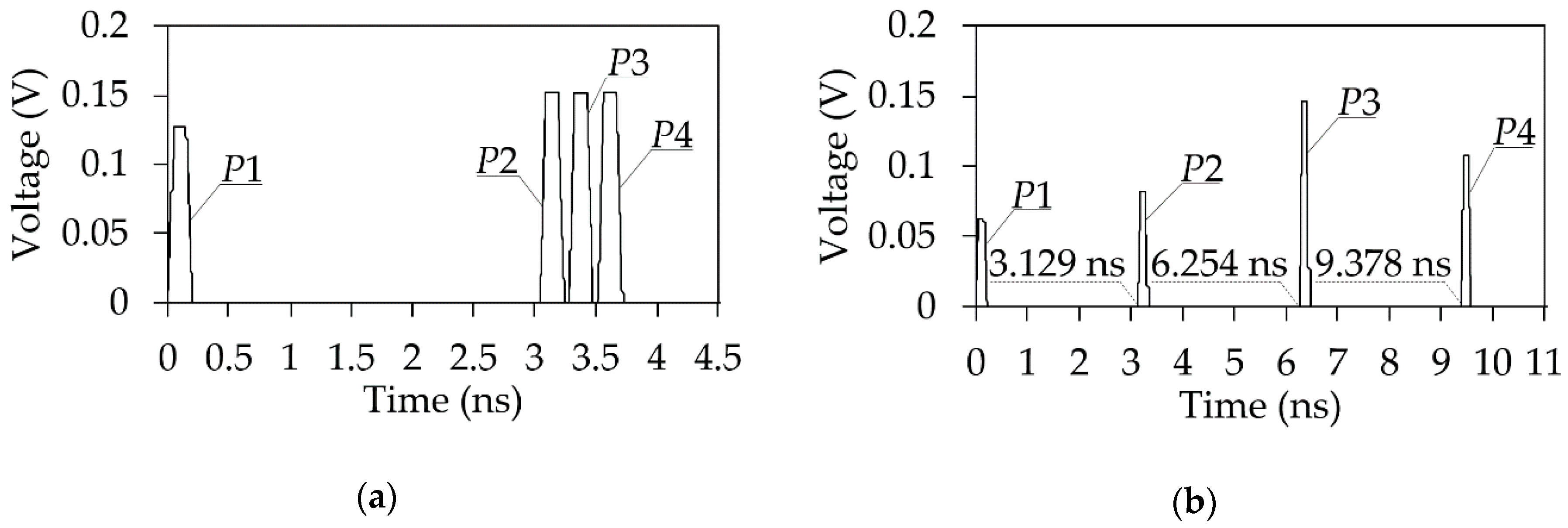
Figure 11.
Voltage waveform at the ML output (a) with optimal parameters and (b) under condition (8).
Figure 11.
Voltage waveform at the ML output (a) with optimal parameters and (b) under condition (8).
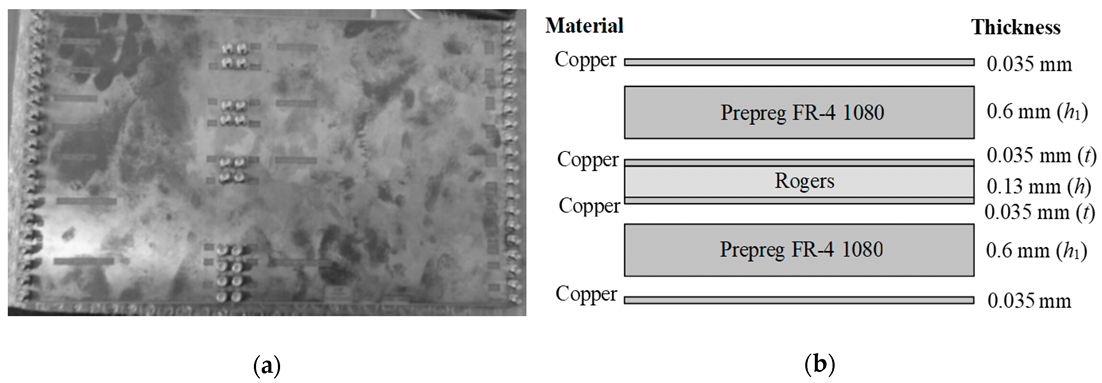
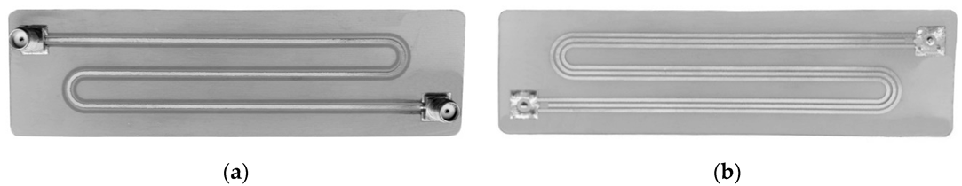
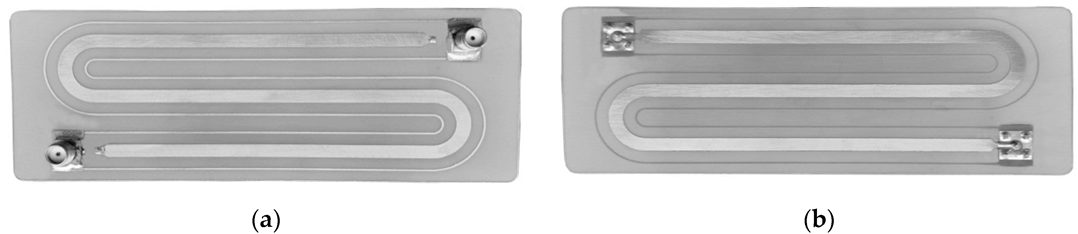
Figure 12.
(a) Photograph of the PCB prototype with modal reservation (MR); (b) PCB stack.
Figure 12.
(a) Photograph of the PCB prototype with modal reservation (MR); (b) PCB stack.
Figure 13.
(a) Cross-section; (b) equivalent circuit of a structure with a single MR; (c) EMF waveform.
Figure 13.
(a) Cross-section; (b) equivalent circuit of a structure with a single MR; (c) EMF waveform.
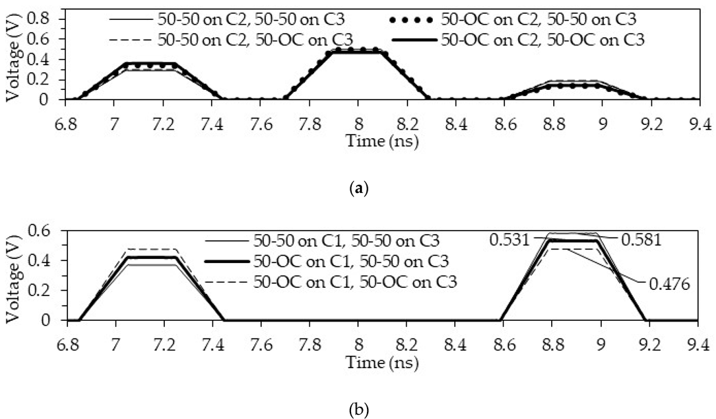
Figure 14.
Voltage waveforms at the near end of the active conductor in the structure with a single MR for (a) 50 Ω, (b) short circuit (SC), (c) open circuit (OC) at the near (-) or far ( = ) end of the passive conductor.
Figure 14.
Voltage waveforms at the near end of the active conductor in the structure with a single MR for (a) 50 Ω, (b) short circuit (SC), (c) open circuit (OC) at the near (-) or far ( = ) end of the passive conductor.
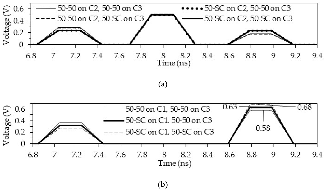
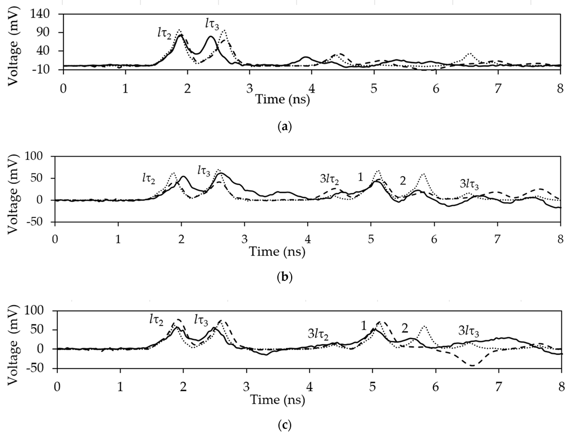
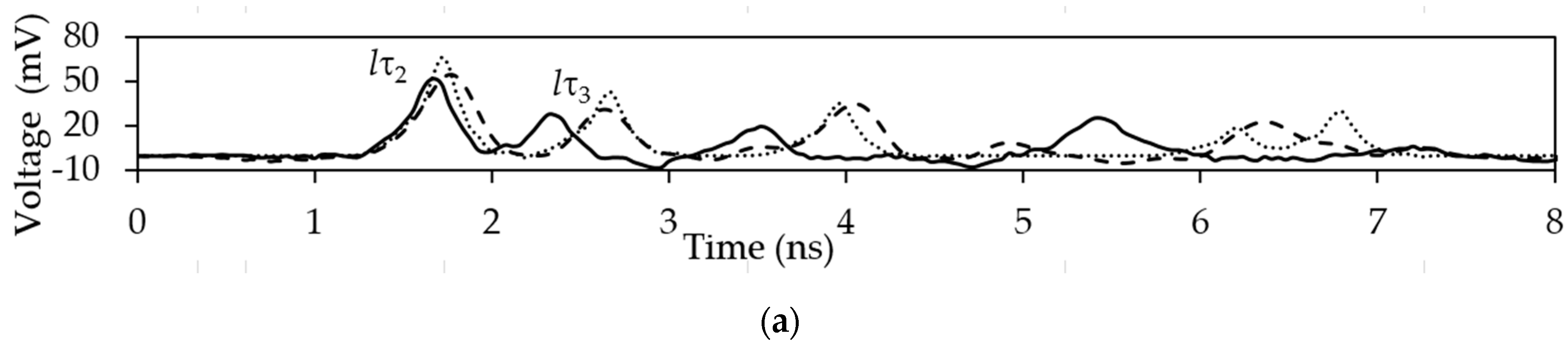
Figure 15.
Voltage waveforms at the far end of the active conductor in the structure with a single MR for (a) 50 Ω, (b) SC, (c) OC at one end of the passive conductor.
Figure 15.
Voltage waveforms at the far end of the active conductor in the structure with a single MR for (a) 50 Ω, (b) SC, (c) OC at one end of the passive conductor.
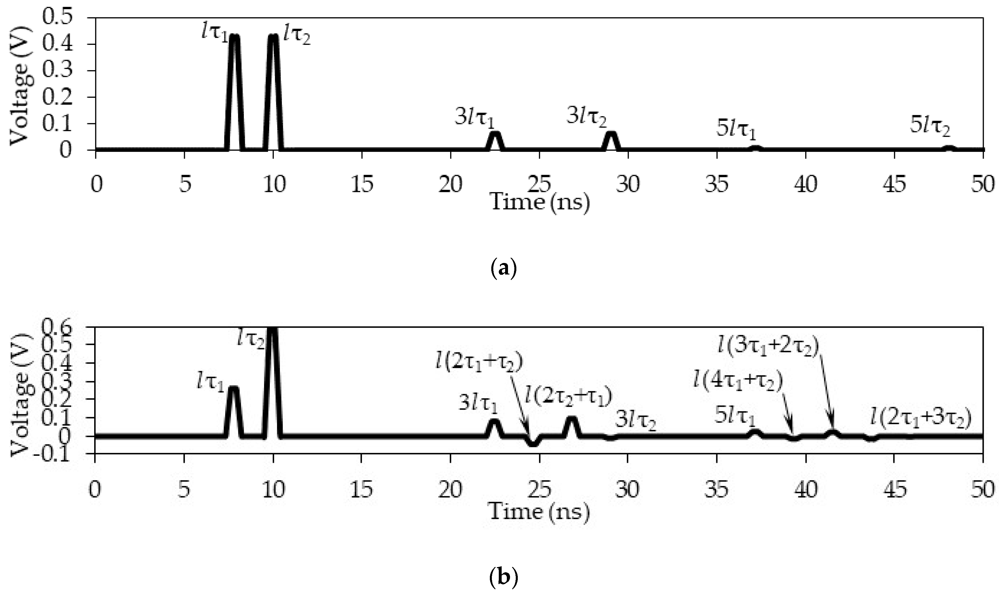
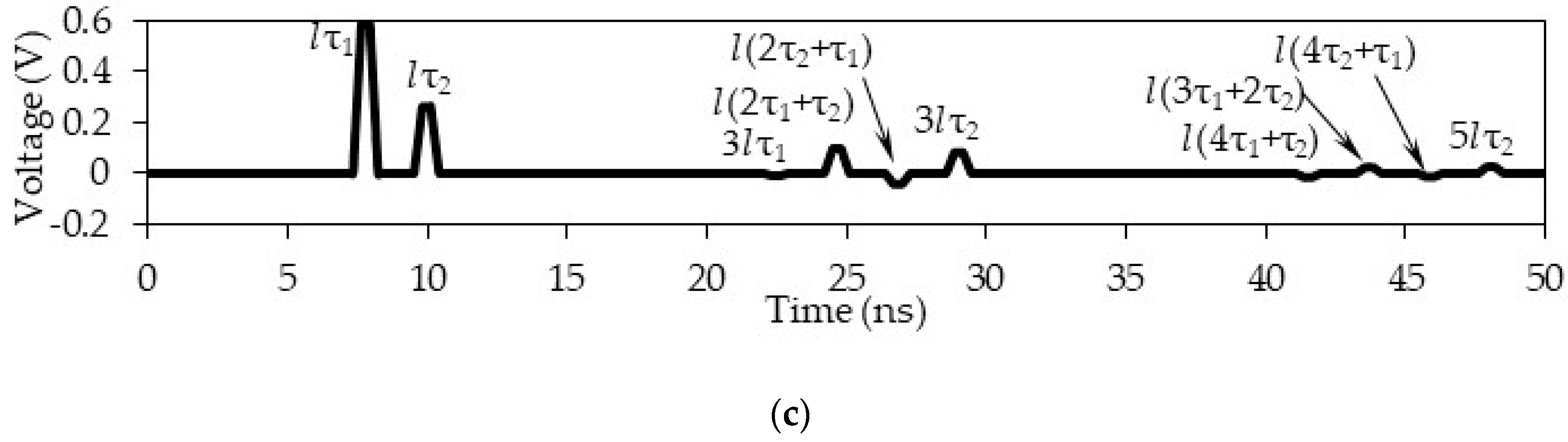
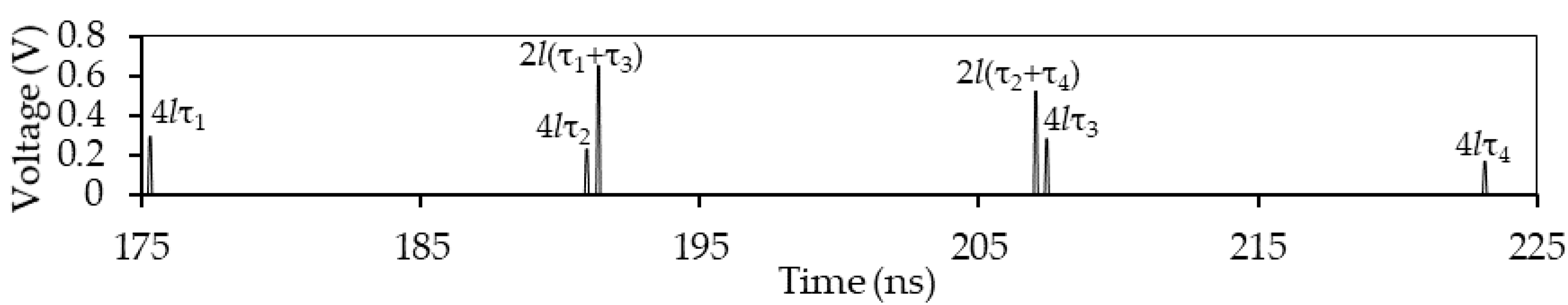
Figure 16.
Voltage amplitudes of each of the pulses at the far end of the active conductor between the delays (a) lτ1 and lτ2, (b) 3lτ1, 3lτ2, l(2τ1 + τ2) and l(2τ2 + τ1), (c) 5lτ1, 5lτ2, l(3τ1 + 2τ2), l(τ1 + 4τ2), l(4τ1 + τ2), and l(2τ1 + 3τ2).
Figure 16.
Voltage amplitudes of each of the pulses at the far end of the active conductor between the delays (a) lτ1 and lτ2, (b) 3lτ1, 3lτ2, l(2τ1 + τ2) and l(2τ2 + τ1), (c) 5lτ1, 5lτ2, l(3τ1 + 2τ2), l(τ1 + 4τ2), l(4τ1 + τ2), and l(2τ1 + 3τ2).
Figure 17.
Cross-section of the three-conductor microstrip structure with an additional dielectric.
Figure 17.
Cross-section of the three-conductor microstrip structure with an additional dielectric.
Figure 18.
Equivalent circuits of the three-conductor structure for (a) extreme and (b) average active conductors.
Figure 18.
Equivalent circuits of the three-conductor structure for (a) extreme and (b) average active conductors.
Figure 19.
Voltage waveforms at the (a) near and far (b) ends of the three-conductor structure with side (-) and middle (- -) active conductors.
Figure 19.
Voltage waveforms at the (a) near and far (b) ends of the three-conductor structure with side (-) and middle (- -) active conductors.
Figure 20.
Voltage waveforms at the far end of the active conductor in the structure with MR for an OC at one end of the passive conductor with active conductors (a) C1, (b) C2.
Figure 20.
Voltage waveforms at the far end of the active conductor in the structure with MR for an OC at one end of the passive conductor with active conductors (a) C1, (b) C2.
Figure 21.
Voltage waveforms at the far end of the active conductor in the structure with an MR for an SC at one end of the passive conductor with active conductors (a) C1, (b) C2.
Figure 21.
Voltage waveforms at the far end of the active conductor in the structure with an MR for an SC at one end of the passive conductor with active conductors (a) C1, (b) C2.
Figure 22.
Equivalent circuit of a reflection symmetric MF.
Figure 22.
Equivalent circuit of a reflection symmetric MF.
Figure 23.
Equivalent circuits of 2 half-turn reflection symmetric ML: (a) 1, (b) 2 and (c) 3.
Figure 23.
Equivalent circuits of 2 half-turn reflection symmetric ML: (a) 1, (b) 2 and (c) 3.
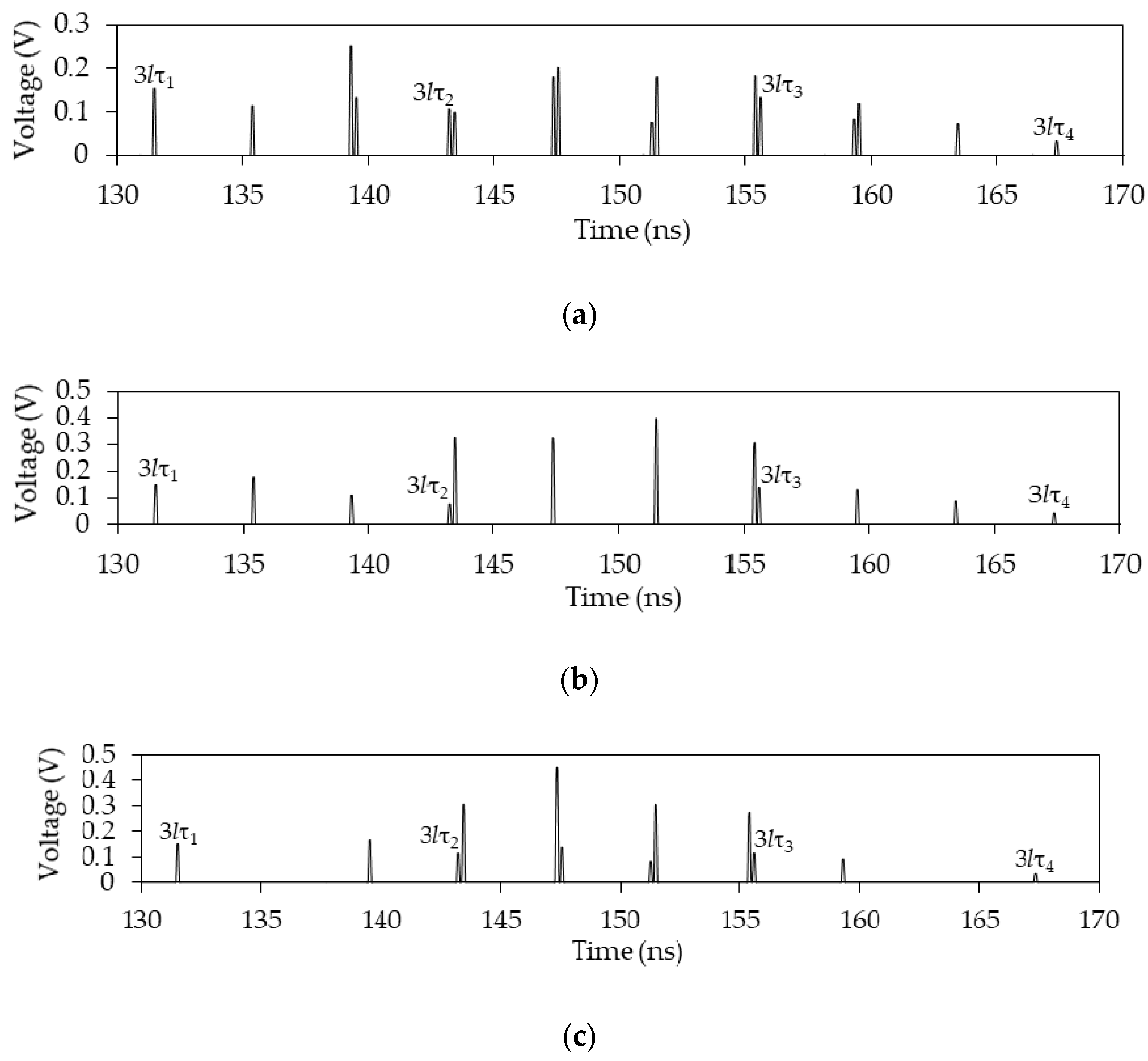
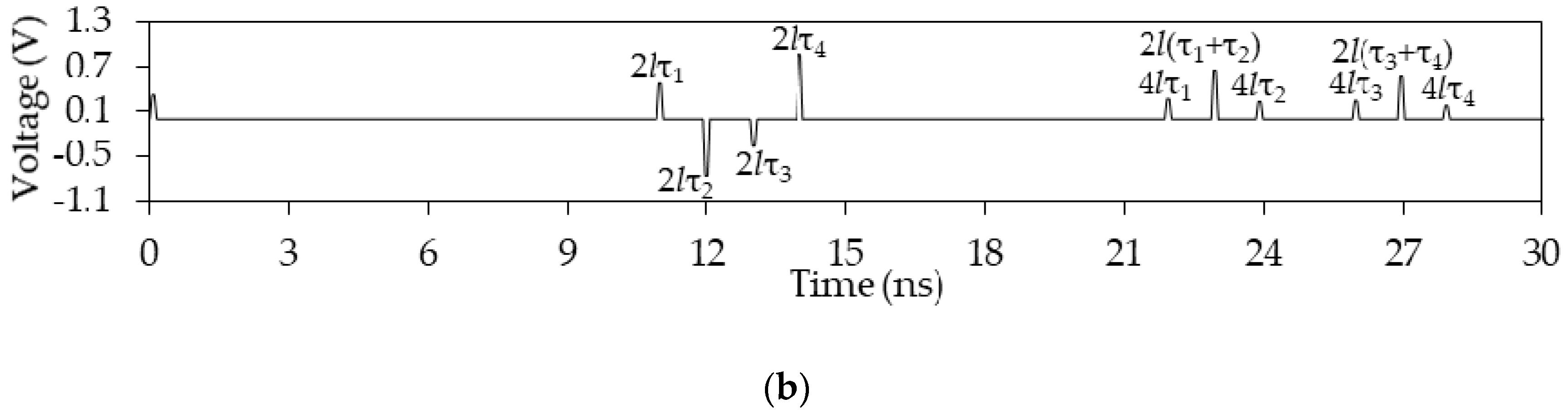
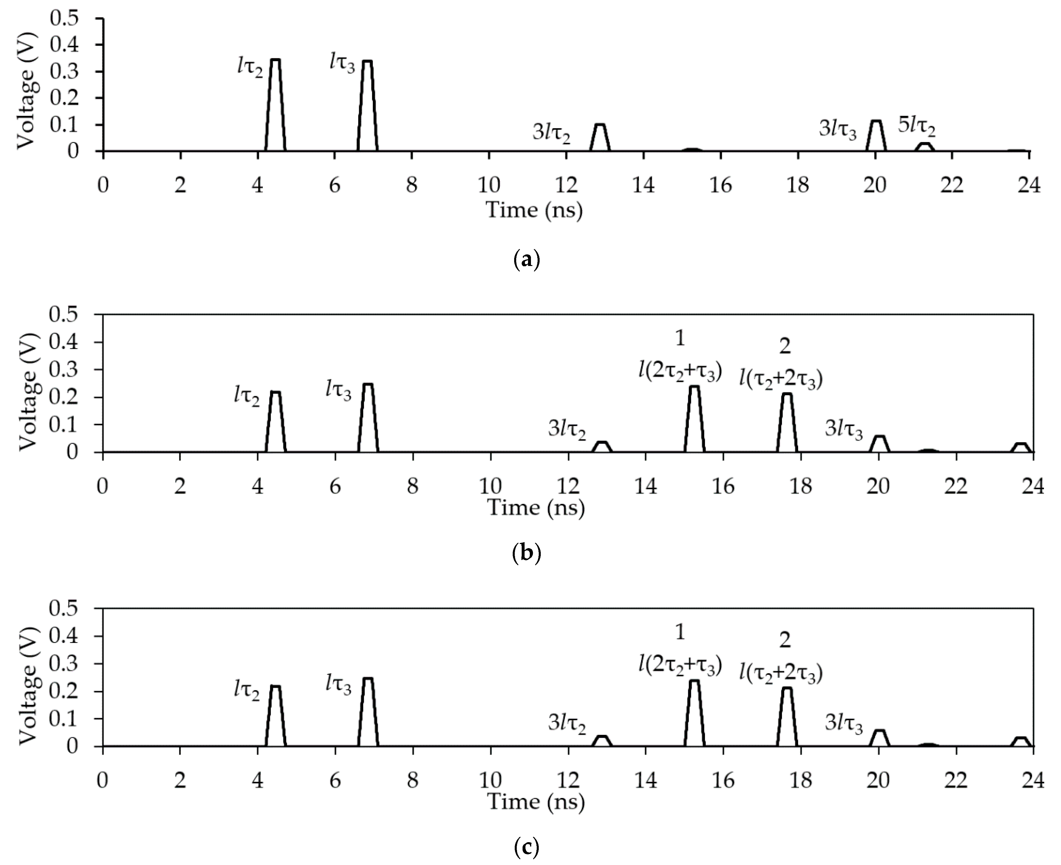
Figure 24.
Voltage waveforms at the output of the 2 half-turn circuits with l = 1 m: (a) 1, (b) 2 and (c) 3.
Figure 24.
Voltage waveforms at the output of the 2 half-turn circuits with l = 1 m: (a) 1, (b) 2 and (c) 3.
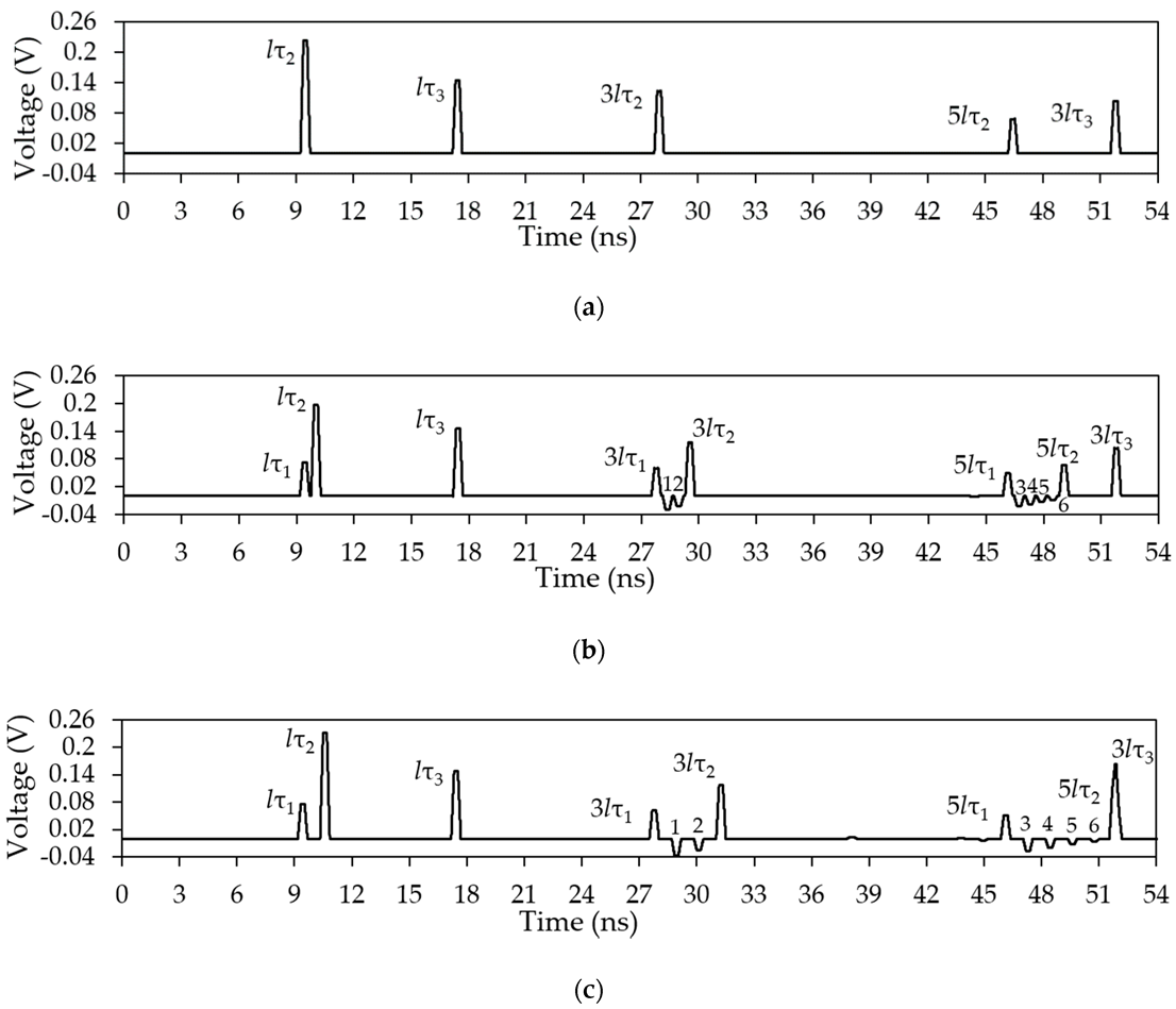
Figure 25.
Voltage waveforms at the output of the 2 half-turn circuits with l = 8 m: (a) 2, (b) 3.
Figure 25.
Voltage waveforms at the output of the 2 half-turn circuits with l = 8 m: (a) 2, (b) 3.
Figure 26.
Voltage waveforms at the output of circuit 2 with l = 8 m and h = 1 mm.
Figure 26.
Voltage waveforms at the output of circuit 2 with l = 8 m and h = 1 mm.
Figure 27.
Equivalent circuits of 3 half-turns reflection symmetric ML: (a) 1, (b) 2 and (c) 3.
Figure 27.
Equivalent circuits of 3 half-turns reflection symmetric ML: (a) 1, (b) 2 and (c) 3.
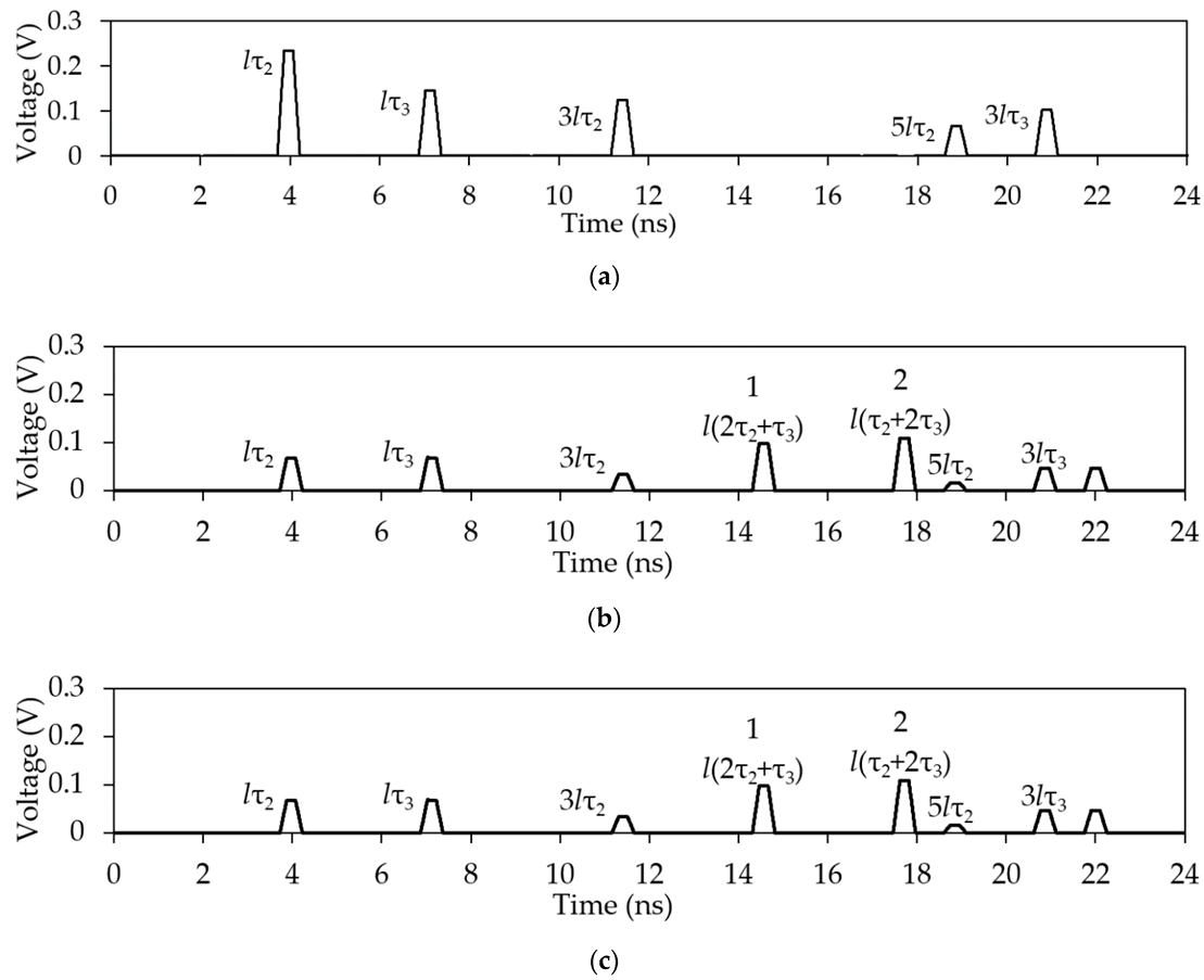
Figure 28.
Voltage waveforms at the output of the 3-half-turn circuits with l = 1 m: (a) 1, (b) 2, and (c) 3.
Figure 28.
Voltage waveforms at the output of the 3-half-turn circuits with l = 1 m: (a) 1, (b) 2, and (c) 3.
Figure 29.
Voltage waveforms at the output of the 3-half-turn circuits: (a) 1, (b) 2, and (c) 3 for l = 8 m.
Figure 29.
Voltage waveforms at the output of the 3-half-turn circuits: (a) 1, (b) 2, and (c) 3 for l = 8 m.
Figure 30.
Voltage waveforms at the output of the 3-half-turn circuits with l = 1 m and h = 1 mm: (a) 2, (b) 3.
Figure 30.
Voltage waveforms at the output of the 3-half-turn circuits with l = 1 m and h = 1 mm: (a) 2, (b) 3.
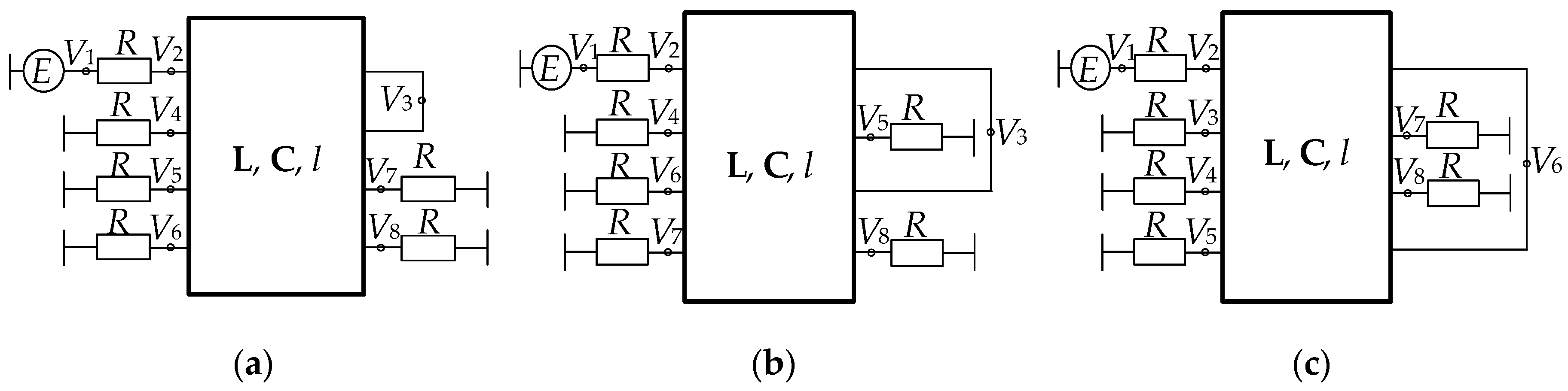
Figure 31.
Equivalent circuits of connecting 4 half-turn reflection symmetric ML: (a) 1, (b) 2.
Figure 31.
Equivalent circuits of connecting 4 half-turn reflection symmetric ML: (a) 1, (b) 2.
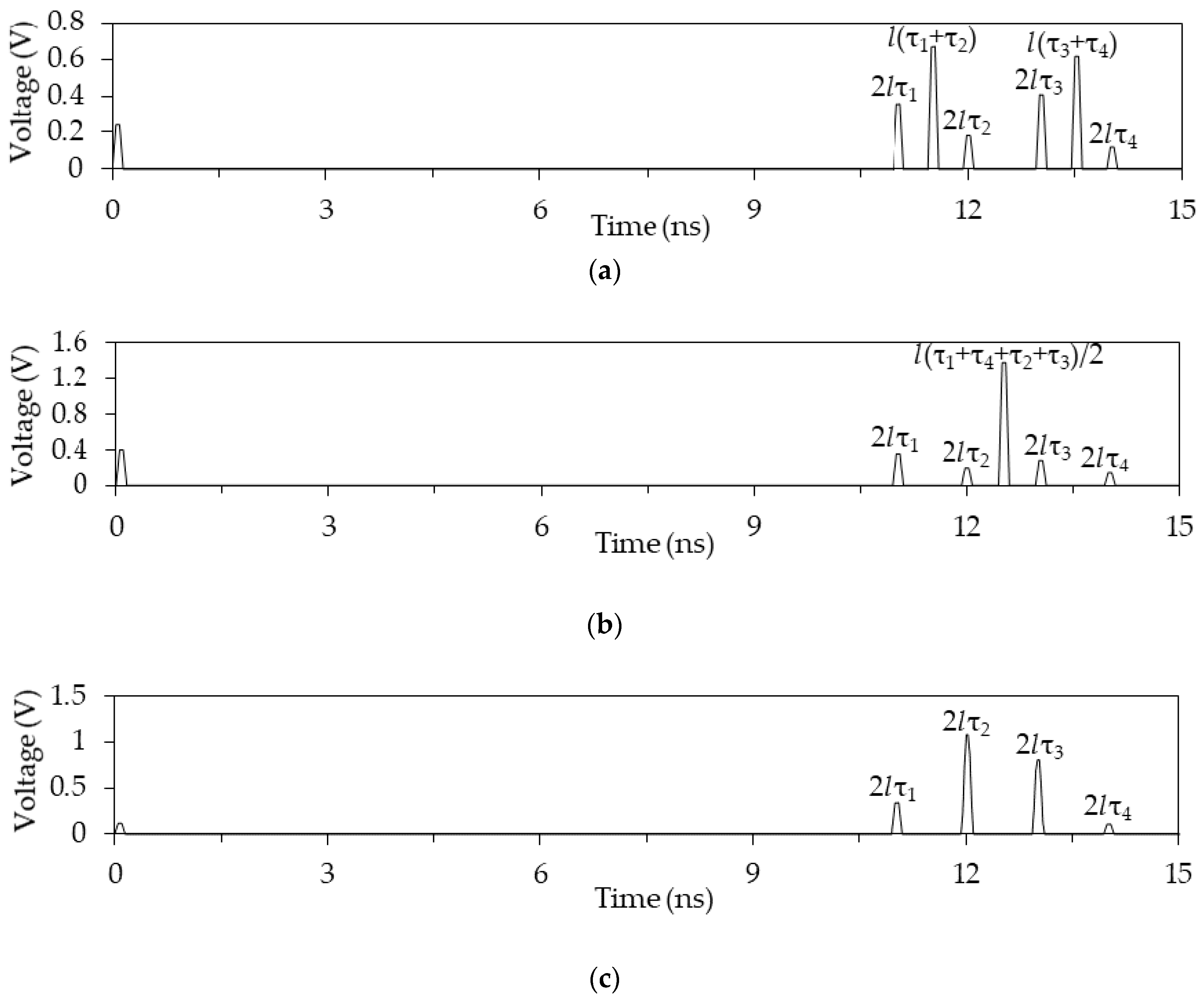
Figure 32.
Voltage waveforms at the output of the 4-half-turn circuits with l = 1 m: (a) 1 and (b) 2.
Figure 32.
Voltage waveforms at the output of the 4-half-turn circuits with l = 1 m: (a) 1 and (b) 2.
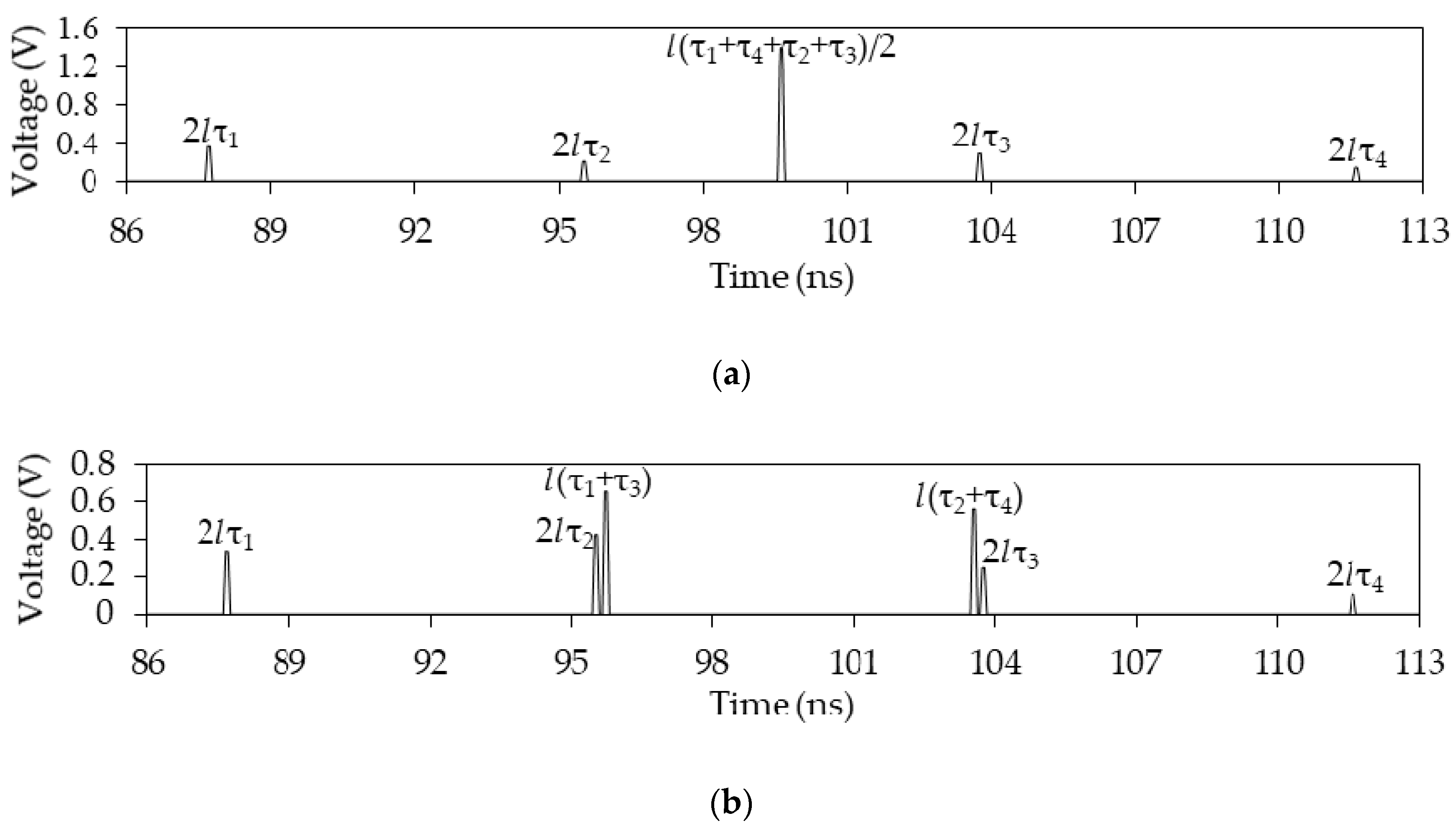
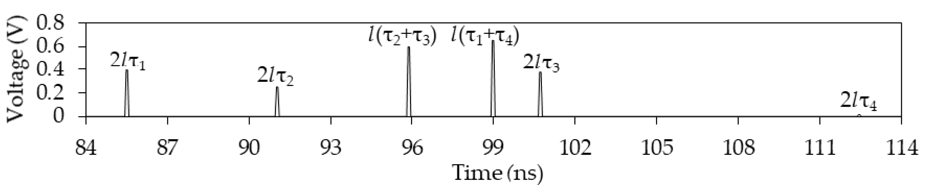
Figure 33.
Voltage waveforms at the output of the 4-half-turn circuit 1 with l = 8 m.
Figure 33.
Voltage waveforms at the output of the 4-half-turn circuit 1 with l = 8 m.
Figure 34.
(a) Cross-section and (b) equivalent circuit of the MF. The conductors: A—active, P—passive, R—reference.
Figure 34.
(a) Cross-section and (b) equivalent circuit of the MF. The conductors: A—active, P—passive, R—reference.
Figure 35.
Voltage waveforms at the MF1 output for (a) R2 = R5 = 50 Ω, (b) OC–SC, and (c) SC–OC.
Figure 35.
Voltage waveforms at the MF1 output for (a) R2 = R5 = 50 Ω, (b) OC–SC, and (c) SC–OC.
Figure 36.
Voltage waveforms at the MF2 output for (a) R2 = R5 = 50 Ω, (b) OC–SC, and (c) SC–OC.
Figure 36.
Voltage waveforms at the MF2 output for (a) R2 = R5 = 50 Ω, (b) OC–SC, and (c) SC–OC.
Figure 37.
Voltage waveforms at the MF output for (a) s1 = 3.5, (b) 1.1, (c) 0.5 mm, and l = 1 m.
Figure 37.
Voltage waveforms at the MF output for (a) s1 = 3.5, (b) 1.1, (c) 0.5 mm, and l = 1 m.
Figure 38.
Voltage waveforms at the MF output (a) s1 = 3.5, (b) 1.1, (c) 0.5 mm, and l = 2.5 m.
Figure 38.
Voltage waveforms at the MF output (a) s1 = 3.5, (b) 1.1, (c) 0.5 mm, and l = 2.5 m.
Figure 39.
Voltage waveforms at the MF output with OC–SC on the passive conductor for (a) s1 = 3.5, (b) 1.1, (c) 0.5 mm, and l = 1 m.
Figure 39.
Voltage waveforms at the MF output with OC–SC on the passive conductor for (a) s1 = 3.5, (b) 1.1, (c) 0.5 mm, and l = 1 m.
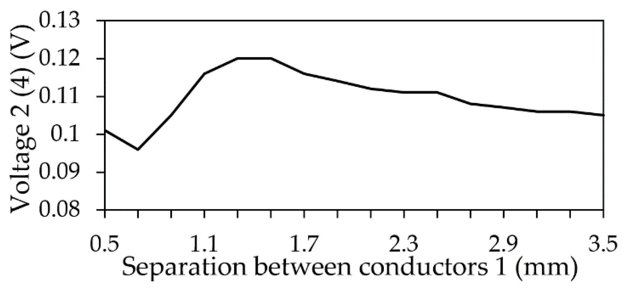
Figure 40.
Dependence of the output voltage amplitude on s1.
Figure 40.
Dependence of the output voltage amplitude on s1.
Figure 41.
Digitized signal of the oscilloscope.
Figure 41.
Digitized signal of the oscilloscope.
Figure 42.
Photomasks of the MF1 layout: (a) top and (b) bottom layers.
Figure 42.
Photomasks of the MF1 layout: (a) top and (b) bottom layers.
Figure 43.
Photomasks of the MF2 layout: (a) top and (b) bottom layers.
Figure 43.
Photomasks of the MF2 layout: (a) top and (b) bottom layers.
Figure 44.
Photos of the MF1 layout: (a) top and (b) bottom layers.
Figure 44.
Photos of the MF1 layout: (a) top and (b) bottom layers.
Figure 45.
Photos of the MF2 layout: (a) top and (b) bottom layers.
Figure 45.
Photos of the MF2 layout: (a) top and (b) bottom layers.
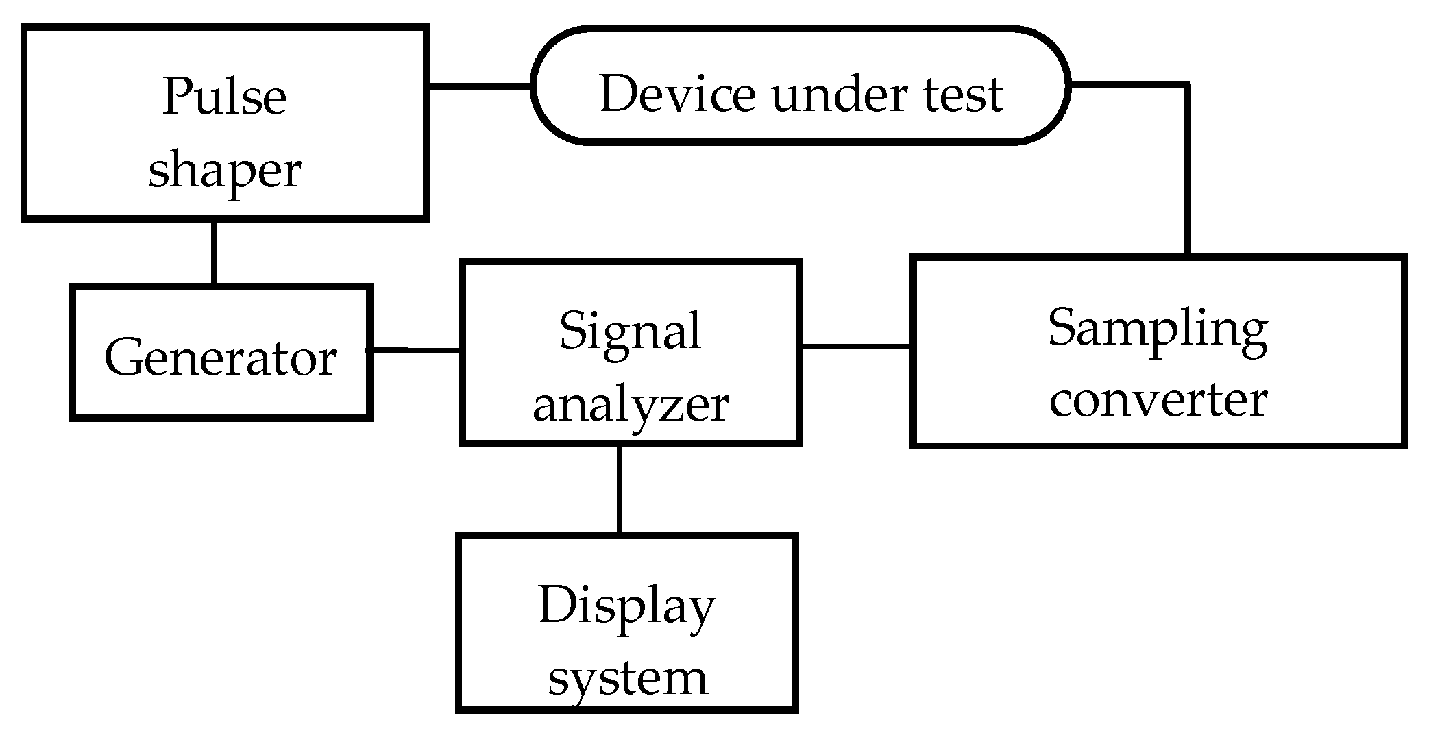
Figure 46.
Experimental setup diagram for the time domain.
Figure 46.
Experimental setup diagram for the time domain.
Figure 47.
Voltage waveforms at the MF1 output obtained during the experiment (––), electrodynamic (– –) and quasistatic (⋅⋅⋅⋅) simulations for (a) R2 = R5 = 50 Ω, (b) OC–SC, and (c) SC–OC.
Figure 47.
Voltage waveforms at the MF1 output obtained during the experiment (––), electrodynamic (– –) and quasistatic (⋅⋅⋅⋅) simulations for (a) R2 = R5 = 50 Ω, (b) OC–SC, and (c) SC–OC.
Figure 48.
Voltage waveforms at the MF2 output obtained during the experiment (––), electrodynamic (– –) and quasistatic (⋅⋅⋅⋅) simulations for (a) R2 = R5 = 50 Ω, (b) OC–SC, and (c) SC–OC.
Figure 48.
Voltage waveforms at the MF2 output obtained during the experiment (––), electrodynamic (– –) and quasistatic (⋅⋅⋅⋅) simulations for (a) R2 = R5 = 50 Ω, (b) OC–SC, and (c) SC–OC.
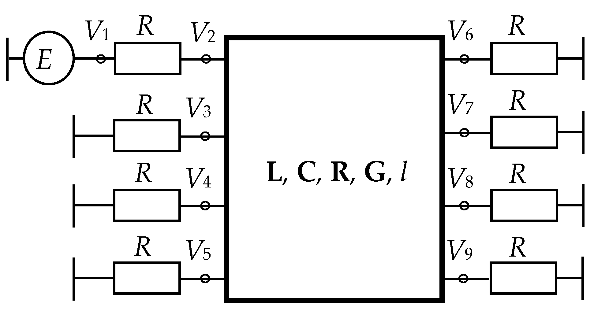
Table 1.
Delays of the main and additional pulses at the near and far ends of the active conductor with SC and OC at the near/far end of the passive conductor.
Table 1.
Delays of the main and additional pulses at the near and far ends of the active conductor with SC and OC at the near/far end of the passive conductor.
| t, ns | U, V |
|---|
| 50 Ω | SC | OC |
|---|
| lτ1 | 7.34 | 0.425 | 0.262 | 0.589 |
| lτ2 | 9.52 | 0.425 | 0.59 | 0.262 |
| 2lτ1 | 14.68 | –0.165 | –0.062/–0.344 | –0.317/0.015 |
| l(τ1 + τ2) | 16.86 | 0 | 0/0.361 | 0/–0.364 |
| 2lτ2 | 19.04 | 0.162 | 0.311/–0.19 | 0.061/0.346 |
| 3lτ1 | 22.02 | 0.063 | 0.0818 | –0.009 |
| l(2τ1 + τ2) | 24.2 | 0 | –0.043 | 0.097 |
| l(2τ2 + τ1) | 26.38 | 0 | 0.097 | –0.043 |
| 3lτ2 | 28.56 | 0.063 | –0.009 | 0.082 |
| 4lτ1 | 29.36 | –0.025 | –0.019/–0.108 | 0.004/0 |
| l(3τ1 + τ2) | 31.54 | 0 | 0/0.114 | 0/0.005 |
| 2l(τ1 + τ2) | 33.72 | 0 | –0.045/0 | 0.045/0 |
| l(τ1 + 3τ2) | 35.9 | 0 | 0/–0.006 | 0/–0.112 |
| 4lτ2 | 38.08 | 0.023 | –0.005/0 | 0.018/0.106 |
| 5lτ1 | 36.7 | 0.009 | 0.026 | 0 |
| l(4τ1 + τ2) | 38.88 | 0 | –0.013 | –0.002 |
| l(3τ1 + 2τ2) | 41.06 | 0 | 0.023 | –0.015 |
| l(2τ1 + 3τ2) | 43.24 | 0 | –0.015 | 0.023 |
| l(τ1 + 4τ2) | 45.42 | 0 | –0.002 | –0.013 |
| 5lτ2 | 47.6 | 0.009 | 0 | 0.026 |
Table 2.
Per-unit length delays (ns/m) for modes 1–4, multiplied by 1, 2, 4, and 16.
Table 2.
Per-unit length delays (ns/m) for modes 1–4, multiplied by 1, 2, 4, and 16.
| Multiplier | 1 | 2 | 3 | 4 |
|---|
| 1 | 5.4698 | 5.9591 | 6.4746 | 6.9687 |
| 2 | 10.9398 | 11.9183 | 12.9493 | 13.9376 |
| 16 | 87.5168 | 98.3456 | 103.5936 | 111.4992 |
| 16 (h = 1 mm) | 85.4332 | 90.9643 | 100.6443 | 112.3761 |
Table 3.
Pulse delays 1–16 (ns) for circuits 1, 2, and 3.
Table 3.
Pulse delays 1–16 (ns) for circuits 1, 2, and 3.
| No | 1 | 2 | 3 | 4 | 5 | 6 | 7 | 8 | 9 | 10 | 11 | 12 | 13 | 14 | 15 | 16 |
|---|
| 1 | 131.4 | 135.3 | 139.2 | 139.4 | 143.1 | 143.3 | 147.2 | 147.4 | 151.1 | 155.3 | 155.3 | 155.5 | 159.2 | 159.4 | 163.3 | 167.2 |
| 2 | 128.1 | 130.9 | 133.6 | 136.4 | 138.5 | 141.2 | 141.6 | 144.3 | 146.1 | 149.2 | 150.96 | 151.96 | 155.0 | 156.8 | 162.7 | 168.5 |
| 3 | 128.1 | 135.7 | 136.4 | 138.5 | 141.2 | 141.6 | 143.3 | 144.3 | 146.1 | 147.1 | 149.2 | 150.9 | 151.9 | 155.0 | 157.8 | 168.5 |
Table 4.
Assumed values of the additional pulse delays equal to the arithmetic mean (AM) value of the two modes 1–4 delays for circuit 1.
Table 4.
Assumed values of the additional pulse delays equal to the arithmetic mean (AM) value of the two modes 1–4 delays for circuit 1.
| AM | 3l(τ1 + τ2)/2 | 3l(τ1 + τ3)/2 | 3l(τ2 + τ3)/2 | 3l(τ1 + τ4)/2 | 3l(τ2 + τ4)/2 | 3l(τ3 + τ4)/2 |
|---|
| t, ns | 137.287 | 143.467 | 149.333 | 149.353 | 161.4 | 155.219 |
Table 5.
Per-unit length delays (ns/m) for modes 1–4, multiplied by 1, 2, 4, and 32.
Table 5.
Per-unit length delays (ns/m) for modes 1–4, multiplied by 1, 2, 4, and 32.
| Multiplier | 1 | 2 | 3 | 4 |
|---|
| 1 | 5.4698 | 5.9591 | 6.4746 | 6.9687 |
| 2 | 10.9398 | 11.9183 | 129.493 | 13.9376 |
| 4 | 21.8795 | 23.8366 | 258.987 | 27.8752 |
| 32 | 175.036 | 190.693 | 207.189 | 223.001 |
Table 6.
Delays (ns) of the main and additional pulses.
Table 6.
Delays (ns) of the main and additional pulses.
| | lτ1 | lτ 2 | lτ 3 | 3lτ1 | 3lτ2 | 3lτ3 | 2l(τ2 + τ3) | l(τ2 + 2τ3) |
|---|
| MF1 | 3.95 | 4.21 | 6.60 | 11.86 | 12.62 | 19.77 | 15.00 | 17.39 |
| MF2 | 3.67 | 3.72 | 6.87 | 11.03 | 11.16 | 20.61 | 14.30 | 17.46 |
Table 7.
Amplitudes (V) of 4 main and 2 additional pulses at the output of MF1 and MF2 for OC–SC and SC–OC.
Table 7.
Amplitudes (V) of 4 main and 2 additional pulses at the output of MF1 and MF2 for OC–SC and SC–OC.
| R2-R5 | MF1 | MF2 |
|---|
| OC–SC | 0.23 | 0.26 | 0.038 | 0.062 | 0.25 | 0.21 | 0.069 | 0.070 | 0.040 | 0.023 | 0.104 | 0.112 |
| SC–OC | 0.22 | 0.25 | 0.042 | 0.064 | 0.24 | 0.22 | 0.071 | 0.071 | 0.037 | 0.023 | 0.111 | 0.101 |
Table 8.
Per-unit length mode delays (ns/m).
Table 8.
Per-unit length mode delays (ns/m).
| s1, mm | τ1 | τ2 | τ3 |
|---|
| 3.5 | 3.658 | 3.695 | 6.872 |
| 1.1 | 3.670 | 3.906 | 6.872 |
| 0.5 | 3.670 | 4.135 | 6.872 |
Table 9.
Arrival times (ns) for mode pulses.
Table 9.
Arrival times (ns) for mode pulses.
| s1, mm | lτ1 | lτ2 | lτ3 | 3lτ1 | 3lτ2 | 3lτ3 | 5lτ1 | 5lτ2 | 5lτ3 |
|---|
| 3.5 | 9.145 | 9.237 | 17.181 | 27.43 | 27.712 | 51.543 | 45.726 | 46.187 | 85.905 |
| 1.5 | 9.176 | 9.764 | 17.181 | 27.529 | 29.292 | 51.543 | 45.883 | 48.821 | 85.905 |
| 0.5 | 9.176 | 10.338 | 17.181 | 27.528 | 31.014 | 51.541 | 45.879 | 51.691 | 85.903 |
Table 10.
Arrival times (ns) for additional pulses.
Table 10.
Arrival times (ns) for additional pulses.
| № | 1 | 2 | 3 | 4 | 5 | 6 |
|---|
| Combination | l(2τ1 + τ2) | l(τ1 + 2τ2) | l(4τ1 + τ2) | l(3τ1 + 2τ2) | l(2τ1 + 3τ2) | l(τ1 + 4τ2) |
| s1 = 1.1 mm | 28.117 | 28.705 | 46.471 | 47.059 | 47.647 | 48.235 |
| s1 = 0.5 mm | 28.69 | 29.852 | 47.041 | 48.203 | 49.365 | 50.527 |
Table 11.
Amplitudes (mV) of additional pulses 1 and 2 at the output of MF1 obtained with various types of analysis.
Table 11.
Amplitudes (mV) of additional pulses 1 and 2 at the output of MF1 obtained with various types of analysis.
| Pulse | Quasistatic | Electrodynamic | Experiment |
|---|
| OC–SC | SC–OC | OC–SC | SC–OC | OC–SC | SC–OC |
|---|
| 1 | 67 | 67 | 47 | 72 | 43 | 51 |
| 2 | 59 | 59 | 18 | - | 22 | 18 |
Table 12.
Amplitudes (mV) of additional pulses 1 and 2 at the output of MF2 obtained with various types of analysis.
Table 12.
Amplitudes (mV) of additional pulses 1 and 2 at the output of MF2 obtained with various types of analysis.
| Pulse | Quasistatic | Electrodynamic | Experiment |
|---|
| OC–SC | SC–OC | OC–SC | SC–OC | OC–SC | SC–OC |
|---|
| 1 | 28 | 27 | 47 | 15 | 10 | 8 |
| 2 | 32 | 28 | 9 | 12 | 13 | 10 |
Table 13.
Per-unit length mode delays (ns/m) and arrival times of mode pulses and additional pulses (ns).
Table 13.
Per-unit length mode delays (ns/m) and arrival times of mode pulses and additional pulses (ns).
| | τ1 | τ2 | τ3 | lτ1 | lτ2 | lτ3 | 3lτ1 | 3lτ2 | 3lτ3 | l(2τ2 + τ3) | l(τ2 + 2τ3) |
|---|
| MF1 | 3.98 | 4.23 | 6.58 | 1.17 | 1.24 | 1.88 | 3.58 | 3.81 | 5.92 | 4.51 | 5.22 |
| MF2 | 3.69 | 3.73 | 6.86 | 1.11 | 1.12 | 2.06 | 3.32 | 3.36 | 6.18 | 4.30 | 5.24 |

 ,
, 


