Article

Detection and Localization of Interference and Useful Signal Extreme Points in Closely Coupled Multiconductor Transmission Line Networks

by
Ruslan R. Gazizov
1,*,
Timur T. Gazizov
2 and
Talgat R. Gazizov
1
1
Television and Control Department, Tomsk State University of Control Systems and Radioelectronics, 634050 Tomsk, Russia
2
Information Technologies Department, Tomsk State Pedagogical University, 634061 Tomsk, Russia
*
Author to whom correspondence should be addressed.
Symmetry 2019, 11(10), 1209; https://doi.org/10.3390/sym11101209
Submission received: 28 August 2019 / Revised: 25 September 2019 / Accepted: 26 September 2019 / Published: 27 September 2019
(This article belongs to the Special Issue Information Technologies and Electronics)

Abstract

:
This study highlights the importance of detecting and localizing useful and interference signal extreme points in multiconductor transmission lines (MCTL) by developing a new approach for detecting and localizing signal extreme points in MCTL networks of arbitrary complexity. A radio-electronic component is presented as a network consisting of a number of connected MCTL sections. Each MCTL section is divided into segments and the number of segments is set by the user. The approach is based on a quasi-static calculation of signal waveforms at any point (segment) along each conductor of an MCTL. The block diagrams of the developed algorithms are presented. Using the approach, a number of investigations have been done which include the following: the signal maximum detection and localization in the meander lines with one and two turns, the influence of ultrashort pulse duration on localization of its extreme points in the printed circuit board (PCB) bus of a spacecraft autonomous navigation system, the influence of ultrashort pulse duration on localization of crosstalk extreme points in the PCB bus, and the simulation of electrostatic discharge effects on the PCB bus. There are also some investigations with optimization methods presented. A genetic algorithm (GA) was used to optimize the influence of ultrashort pulse duration on localization of the pulse and crosstalk extreme points in the PCB bus. Furthermore, the GA was used to optimize the PCB bus loads by criteria of the peak voltage minimization. A similar investigation was carried out with the evolution strategy. The obtained results help us to argue that the signal extreme points can be detected both in structures with different configurations and applying different excitations.

1. Introduction

The increasing complexity of devices being developed and physical processes occurring in them make a mathematical simulation very important, in particular, because a full-scale simulation is more expensive than a mathematical simulation. Moreover, a lot of conductors create various crosstalk noises and parasitic couplings which complicate the process of diagnosing radio-electronic equipment (REE) because of the necessity to take into account all couplings between conductors [1]. It is important for the diagnostics to be carried out at the designing stage and be aimed at detecting possible vulnerabilities of printed circuit boards (PCB), for example, detecting the places with an excess of voltage or current amplitudes [2,3]. Timely and accurate application of a mathematical simulation would exclude the influence of electromagnetic interference (EMI) on high sensitive equipment during its operation [4], as well as decrease the consequences of intentional EMI which make the REE inoperative [5,6]. Ultra-wideband pulses, power ultrashort pulses [7], and electrostatic discharge (ESD) [8] can be referred to as such excitations. Due to this fact, it is necessary to take into account both useful and interference signals during the PCB diagnostics. Moreover, it is particularly important in the field of aerospace because a fault that appears in one of the parts of aircraft equipment can cause the loss of an aircraft [9,10]. For example, the new method of hardware-in-the-loop simulation for an aircraft electric power system has been presented in [11] and the use a new fault diagnostic method by multi sensor fusion for testing spacecraft control system sensors has been proposed in [12]. In addition, the noises (crosstalk) generated by the useful signals, the powerful intentional electromagnetic pulses of nanosecond and subnanosecond ranges, are dangerous because they are capable of penetrating into various electronic equipment and disabling them. This is important for supporting the uninterrupted operation of critical systems, for example, to assess the situation of electromagnetic terrorism manifestations that have powerful electromagnetic effects on the electrical network, or to protect special technical buildings from external electromagnetic effects. The propagation of such signals in multiconductor transmission lines has been well studied, however, the features of the ultrashort pulse propagation along the conductors with a high density of PCB interconnects are not clearly understood and can lead to their uncontrolled propagation, whereby it is important to provide the control of signal propagation along the entire length of the conductors.
The way to determine the propagation path of noise using the source modulation technique was reviewed in [2], which considered the key parameters and the main properties of the noise source modulation technique (NSMT) based on the amount and the type of modulation of the noise at the victim location. The experiment was performed under ideal conditions, in which two cables had the same common-mode currents, but only one of them was a noise propagating path for the victim. By comparing the propagation path index with the measured insertion loss between the cables and receiving antennas, the NSMT was proved to determine the noise propagation path. Quantifying EMI was examined in [3], namely a methodology for determining and quantifying radiation for practical design guidelines. Due to tight EMC standards, it becomes increasingly important to diagnose the radiation hot spot in the radiation process before applying attenuation measures. The researchers implemented the analysis of characteristic mode together with the integral equation based numerical method in order to identify the hot spots for EMI radiation. Several numerical examples were applied to benchmark the proposed approach. An analysis in time domain and simulation of crosstalk noise reduction for high-speed digital circuits by a guard trace with an open stub between coupled striplines was carried out in [13]. In order to mitigate the interference of crosstalk noise in PCBs or packages the grounded guard traces were utilized. The study included a discussion on how the guard trace with inserted coupled striplines with an open stub affects the crosstalk noise. A design curve for the geometric parameters of coupled striplines inserted guard trace stub was constructed based on the proposed method. The maximum reduction in crosstalk noise in the presented examples exceeded 50%. A new method for the fast-transient analysis of large linear chains using stable high-order methods was presented in [14]. A new algorithm based on the A-stable and L-stable high-speed integration methods in the time domain for simulating large linear circuits was presented. The proposed method took advantage of the mathematical description of the circuits found in these cases in a special form to significantly reduce computational costs. Several variants of schemes were presented to demonstrate the acceleration achieved by the proposed algorithm.
The optimization by means of different methods based on collective intelligence to different application areas has been widely used. For example, a genetic algorithm (GA) with real number encoding was used for structural damage detection based on vibration data in [15]. The objective function was minimized by directly comparing the changes in the measurements before and after damage. Three different criteria were considered, namely, the frequency changes, the mode shape changes, and their combination. All the damaged elements could be detected accurately by genetic algorithm, as seen from the numerical results, even when the analytical model was not accurate. A particle swarm optimization algorithm was used for the quantization thresholds in [16]. The authors considered decentralized detection of an unknown signal corrupted by zero-mean unimodal noise via wireless sensor networks. The asymptotic performance analysis of the multi-bit Rao test was provided and exploited to propose a (signal independent) quantizer design approach by maximizing the noncentrality parameter of the test statistic distribution. Numerical results were provided to show the effectiveness of the Rao test in comparison to generalized likelihood ratio test and the boost in performance obtained by (multiple) threshold optimization. A GA was used for mobile robot localization using ultrasonic sensors in [17]. The researchers investigated an ultrasonic sensor localization system for autonomous mobile robot navigation in an indoor semi-structured environment. They developed a self-localization module which has been integrated successfully in a more complex navigation system. A method for the joint optimization of radio and computing resources for multichannel mobile computing was proposed by [18]. This study, considered a multiple-input multiple-output (MIMO) multicell system where several mobile users ask for computation offloading to an ordinary cloud server. The resulting optimization problem was nonconvex. Nevertheless, in the case of a single user, researchers were able to calculate the main optimal solution in closed form. In the more challenging scenario with an increasing number of users, they suggested an iterative algorithm, which was based on a novel successive convex approximation approach, converging to a local optimal solution of the original nonconvex task. Numerical results showed that the proposed approach excelled the other optimization methods. The projection matrix was optimized for sparse signals in structured interference in [19]. The researchers considered the problem of estimating a signal which has been corrupted with structured noise and proposed an approach for the design optimization of the projection matrix, in which the objective was not only to decrease the amount of data to be processed but also to eliminate the undesired signal components. As a result, they reduced the computation time and the error on the estimation of the unknown parameters of the sparse model, with respect to the uncompressed data. The joint optimization of data and energy transfer in multiuser MIMO systems was performed in [20]. The researchers presented a method to solve the nonconvex optimization task that appeared when constructing the transmit covariance matrices in multiuser MIMO broadcast networks with implementation of simultaneous wireless information and power transfer. Two different approaches were applied to reformulate the (nonconvex) multiobjective problem. In order to solve the resulting formulations, the researchers proposed using the majorization-minimization approach. A method for optimizing the received signal strength (RSS) using the Gauss method was presented in [21]. The optimal RSS threshold was found through minimizing the best achievable localization root mean square error formulated with the aid of fundamental lower bound analysis. The resulting optimal RSS threshold enabled enhanced performance of new fashioned low-cost and low-complex proximity report-based positioning algorithms. A synthesis of a control system based on multicriteria optimization using a GA was presented in [22] in which an approach for the parametric synthesis of the automatic control system (ACS) was suggested. The approach used the genetic algorithm that carries out an approximation of Pareto-optimal solution sets and it was shown that their approach obtained a reasonable solution in a shorter time and with less computational costs than other methods. In [23] optimization was considered using a GA, optimization by the particle swarm method and optimization by the firefly algorithm when designing antennas, and demonstrated the application of the evolutionary optimization methods with multiple objectives to the microstrip antennas constructing. Impedance matching and gain improvement were optimized over a predefined frequency range, resulting in a very small and compact 12 mm x 21 mm ultra-wideband antenna which was fabricated and measured. For radio-electronic equipment optimization the most popular are GAs and evolution strategies (ES) [24]. For example, a new algorithm for optimizing a direct eye diagram for an arbitrary transmission line using a finite impulse response (FIR) filter was proposed in [25] in which a new design algorithm, which directly optimizes the eye diagram using the FIR filter as transmitter pre-emphasis, was proposed to counteract the intersymbol interference in the high-speed data transmission. In order to minimize the resistance of electrical contact, a method for controlling the location of microcontacts based on a GA was proposed in [26]. In this study, the positioning and sizing optimization of microcontact spots were investigated in relation to minimizing the ECR. The optimal solutions were obtained by a novel method of a real-coded genetic-algorithm implemented with a subpopulation-based selection method and a normal distribution probability-based crossover. A method for analyzing and optimizing signal integrity for complex circuits with multiple inputs and outputs based on the analysis of S-parameter data was proposed in [27]. The proposed data mining approach considered both the interconnect structure and the stimulated pattern of a MIMO system, which can carry out thoughtful analysis and optimization with high efficiency. The decentralized dynamic optimization of voltage management in the power supply network was investigated in [28]. By simulating the network dynamics using an autoregressive process and considering time-varying resource constraints, the researchers provided an error bound in tracking the instantaneous optimal solution to the quadratic error objective. The design of the circuit of the delay lines using a GA to minimize crosstalk noise was investigated in [29]. The paper highlighted a development of a design methodology of delay line layout for minimizing crosstalk with the use of a GA for optimization. The GA required a large number of function evaluations, and efficient calculation of crosstalk was proposed together with a new approach of generating random line, making offsprings, and mutation. Different optimum results have been obtained for different objectives and compared.
The quasi-static approach is widely used for analyzing PCB interconnects, because the accuracy of the circuit analysis is often unacceptable, while the electromagnetic analysis often involves large computational costs. The investigations of techniques for detecting and localizing signal extreme points have been performed for single and coupled [30,31] transmission lines, and for a PCB bus of a spacecraft autonomous navigation system (ANS) [32,33], also with the use of a GA [34,35]. The voltage maximum exceeding the signal amplitude at the input by 1.14 times is detected in the meander line with two turns. The voltage maximum, twice as big as the signal amplitude at the input, is detected in the microstrip cross section. The voltage maximum exceeding the steady state level by 18% is detected in the PCB bus of a spacecraft autonomous navigation system. The voltage maximums exceeding the steady state level by 36% and 38% are revealed in the PCB bus by using the GA for optimization. The voltage maximum exceeding the steady state level by 20% is detected in the PCB bus by using the ES optimization.
However, an approach combining the opportunity to perform the diagnostics for detecting and localizing signal extreme points and the optimization of obtained results has not been developed. Therefore, the purpose of this paper is to develop the approach and to demonstrate some recently obtained and new results of applying this approach in detecting and localizing extreme points of useful and interference signals which are necessary for REE diagnostics.
The paper is organized as following. In Section 2, a brief theory is presented. In Section 3, a description of the proposed approach for detecting and localizing signal extreme points is presented. In Section 4, block diagrams of the developed algorithms for the approach are shown. The results of the investigation of coupled transmission lines are presented in Section 5. In Section 6, the results of the investigation of the spacecraft ANS bus are considered. In Section 7, the results of the GA for optimization are shown. In Section 8, the results of the GA for optimization are shown. Section 9 is the conclusions.

2. Theory

The theoretical bases and algorithms for calculating quasi-static responses along each conductor of each multiconductor transmission line (MCTL) section connected to the multiconductor network were developed earlier and presented in [30]. But it seems to be important to show them again for a full understanding of the approach.
Frequency domain equations are used for calculating voltage and current responses in an MCTL section:
V ( x ) = S V ( E 0 C 1 + E D C 2 )
I ( x ) = S I ( E 0 C 1 E D C 2 )
where SV and SI are the matrices of modal voltages and currents; E0 and ED are the diagonal matrices E0 = diag(exp(– γ 1 x), …, exp(– γ N k x)) and ED = diag(exp(– γ 1 ∙(lx)), …, exp(– γ N k (lx))); γ N k is the propagation constant for the k-th MCTL section; Nk is a number of conductors in the k-th MCTL section; l is the length of MCTL section; and x is the coordinate along the MCTL section (the number of x is defined by nTLS parameter). The calculation of SV, SI, and E(x) is described in [36]. C1 and C2 are constant vectors calculated as:
[ C 1 C 2 ] = [ S V S V E ( l ) S V E ( l ) S V ] 1 [ V ( 0 ) V ( l ) ]
where E(l) = diag(exp(– γ 1 l), exp(– γ 2 l), … exp(– γ N k l)); V(0) and V(l) are vectors describing the voltage at the ends of the MCTL section, determined after solving the equation for the circuit with n MCTL sections with lumped elements at the ends:
V = ( s W + H + k = 1 n D k Y k D k t ) 1 E
where s = jω, where ω is angular frequency; W and H are matrices of order A × A describing the lumped memory and memoryless elements of the network, respectively (A is the number of parameters, which are calculated by the modified node potential method); D k = [ i ,   j ] with entries l i , j {0, 1}, where i {1, …, Nk}, j {1, …, 2Nk} with one nonzero value in each column, is the selector matrix that maps the terminal currents of the k-th MCTL section; Y k is the conductance matrix of the k-th MCTL section; V is the vector of the node voltage waveforms; and E is a constant vector with the entries determined by the independent voltage and current sources.
The description of the response calculation algorithm is presented in [36]. By applying the forward fast Fourier transformation (FFT), the original excitation in the time domain is transformed into the frequency domain. Then, calculations of Equations (1) to (4) are carried out. Then, by applying the inverse FFT, the obtained result is transformed into the time domain.

3. Proposed Approach for Signal Extreme Points Detection and Localization

On the basis of the theory presented in Equations (1) to (4), an approach for signal extreme points detection and localization was developed. The description of the approach is presented further. First, an REE developer should make a correct circuit diagram of a structure under development. Then, he should choose a fragment in one of the conductors of the structure to be diagnosed. The diagnostics is aimed at checking whether the amplitudes of a propagating signal exceed the maximum agreed value or how the signal waveform is transformed during the propagation. The chosen fragment can consist of several segments of transmission lines or can be chosen over the whole conductor. In addition, the fragment can be located at any conductor of the structure (the developer can perform the diagnostics of the active or passive conductors to analyze the signal or crosstalk waveforms propagation respectively).
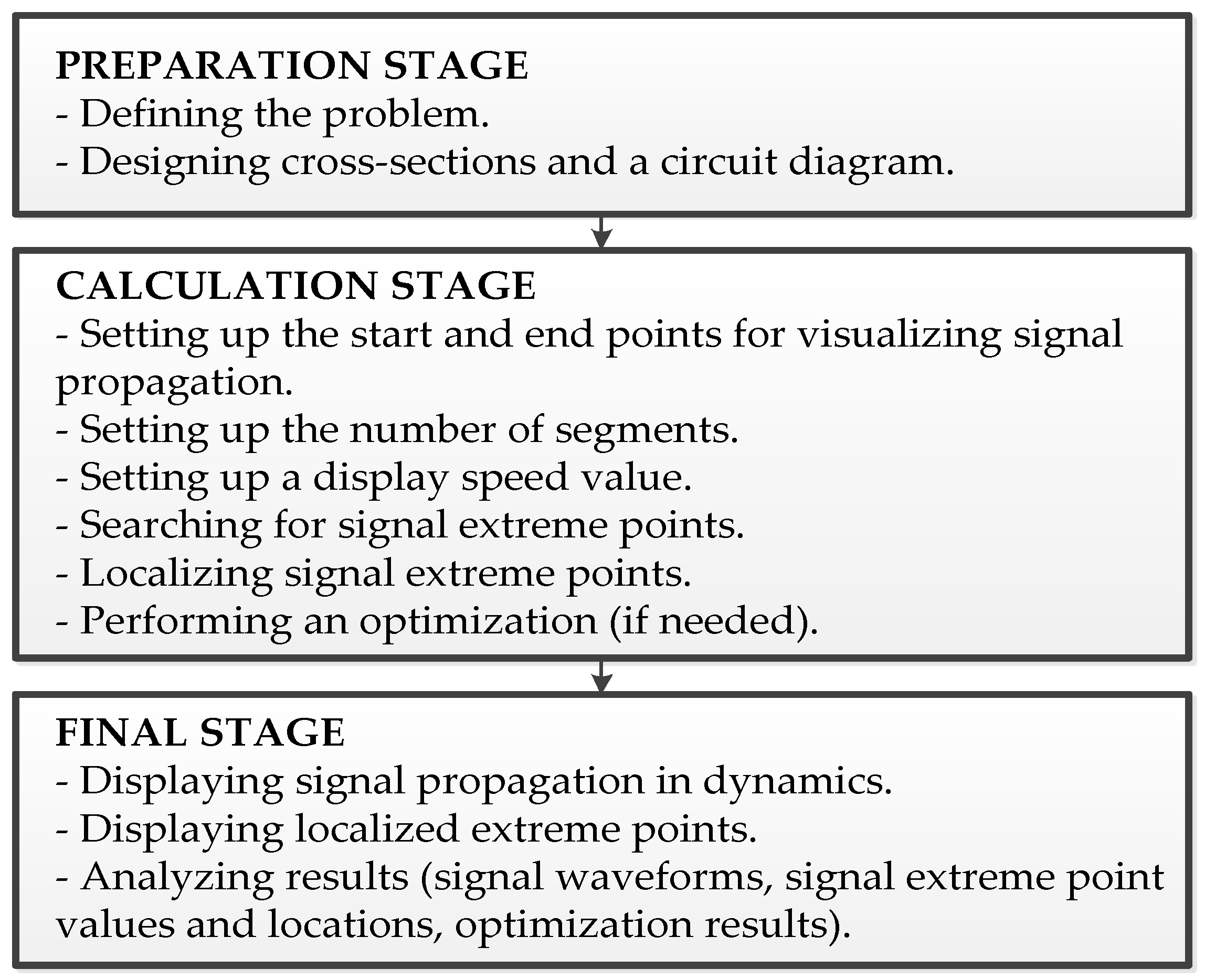
Thus, the proposed approach includes the following stages:
Preparation stage Formulating a problem to be solved, the aim, and expected results. Designing cross sections and a circuit diagram of REE (taking into account all galvanic connections between circuit diagram components), adding all parameters of active and reactive components (for a transmission line section, the per unit length coefficient matrices of electromagnetic (L) and electrostatic (C) induction, conductivities (G), and resistances (R); for the excitation signal source, the type of a signal and its parameters).
Calculation stage Setting up the start and end points of the pulse propagation, the number of a segment along each MCTL section, and the speed of displaying. Calculating signal waveforms. Detecting and localizing signal extreme points. Performing optimization to obtain an optimal solution.
Final stage Analyzing the obtained results, i.e., signal waveforms, whose propagation along each conductor of each MCTL is displayed in dynamics; detected signal extreme points; localization of these points in the circuit diagram.
Let us consider the calculation and final stages in detail. In the calculation stage, to choose the fragment of the conductor (or the whole conductor) that consists of several MCTL sections, the developer should set the start and end points in the circuit diagram. The diagnostics and visualization of the signal propagation will be done along this fragment. Each MCTL section is divided into a number of segments which are set by the developer. The signal waveform is calculated in each segment of each MCTL section. The response (signal waveforms) calculation algorithm differs from the algorithm described in [36] primarily in the fact that it uses segment coordinates instead of a node number. As a result, the system stores voltage or current values calculated in each segment of each conductor section. Then, the signal propagation way along the chosen conductor is defined taking into account all galvanic connections between MCTL sections (in other words a successive display of the signal waveforms calculated in each MCTL segment). The speed of the display is also defined by the developer. Then, the search for signal extreme points is carried out in each segment. It should be mentioned that we need to find not all extreme points but the global (relative to all segments) maximum and minimum only. The numbers of the segment and the MCTL section are assigned to the global maximum or minimum. These numbers are then used for localizing the extreme points. Moreover, there is an opportunity to apply the GA for optimization in this stage, for example, if a user needs to define such excitation pulse duration at which the maximum value of the signal amplitude along the conductor will be the highest.
In the final stage, dynamic visualization of the signal propagation along the conductor is performed. The developer can control the visualization as follows: stop the animation, display the signal waveform in the previous and next segment, and continue the animation. The developer can also push a button with an extreme point to display the signal waveforms with the global extreme point (maximum or minimum). These results are displayed in another window of the program. At the same time, the segments with the calculated signal waveforms are displayed as points in the circuit diagram (according to the signal waveform animation). The animation in the circuit diagram stops when the signal extreme point is displayed, and therefore one can see the place where the extreme point is located. Thus, the developer can perform the diagnostics aimed at checking what global extreme voltages or currents have been detected, where they are localized, and how the signal waveforms have been transformed during its propagation along the conductor. A block diagram of the proposed approach is presented in Figure 1.

4. Developed Algorithms used in the Approach

There are three algorithms which were devised while developing the approach. They are the visualization algorithm of signal propagation along the circuit, the algorithm for defining the allowed ways of signal propagation along the circuit, and the algorithm for detecting and localizing signal extreme points.

4.1. Visualization Algorithm of Signal Propagation along the Circuit

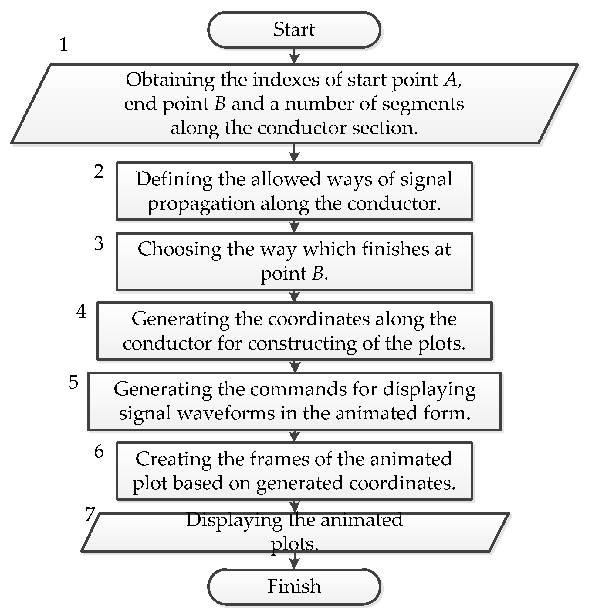
A block diagram of this algorithm is presented in Figure 2. Let us consider the essence of the algorithm. At first, step 1, you should choose the start node A and the end node B between which the visualization of a signal propagation will be shown. Then, step 2 (considered as the algorithm in detail in Section V) defines the propagation way based on these nodes, a number and also an order of MCTL sections and also an order of its segments. The segments’ order will be used in the visualization of signal propagation. As a result of this algorithm, the system generates some commands and performs dynamic visualization.

4.2. Algorithm for Defining the Allowed Ways of Signal Propagation along the Circuit

A block diagram of this algorithm is shown in Figure 3.
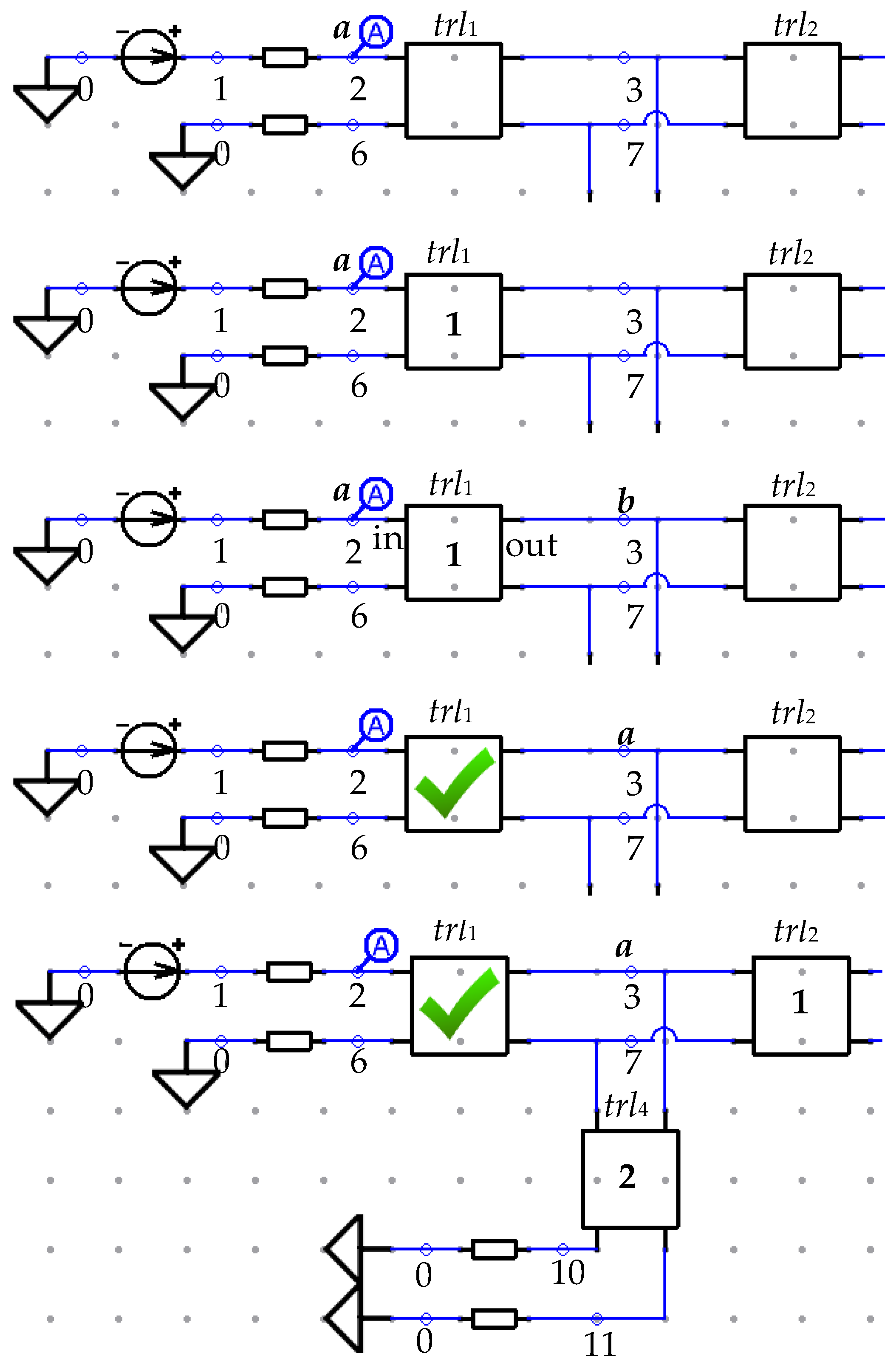
Point A can be chosen at any node of the circuit diagram, but the allowed locations of node B are defined by the algorithm for defining the allowed ways of signal propagation along the circuit. The aim of the algorithm is to provide a condition for maintaining galvanic connections between the MCTL sections on the way of signal propagation. A test circuit diagram is shown in Figure 4. All the parameters of the circuit components are not shown in Figure 4, Figure 5, Figure 6 and Figure 7 because they are not important in this part. MCTL sections in these Figures are called “trl”. The circuit diagram configuration has the primary meaning. Each step of the algorithm before the complete processing of the first circuit component is shown in Figure 5.
Let us consider each step of the algorithm according to the test circuit diagram as follows:
(1)
The index of node A appears in the system (when a user chooses it). A = 2.
(2)
The variable of the list type called “list” is created (empty at first). The start node index is assigned to a current node index a (a = A = 2).
(3)
The circuit components connected to node a are numbered.
(4)
The check of other unprocessed components is performed. If there is an unprocessed component, then go to step 5, otherwise, go to step 7. (Numbers of the steps are shown in Figure 3.)
(5)
The processing of each numbered component is performed in succession. The component end connected to the node a is defined as input and the opposite one is defined as output.
(6)
The index of the node connected to the output end is assigned to node b (b = 3).
(7)
The node a index is added to the end of the “list” (list contains 2).
(8)
The check of another node with b index is performed. If there is a node with b index, then go to step 9, otherwise, go to step 11.
(9)
There is a node with b index. The index of node b is translated to the node a index (a = 3).
(10)
The current numbered component (trl1) becomes completed (shown by green ticks in Figure 5). Other elements connected to node a are numbered again. Therefore, we go to step 3 of the algorithm.
(11)
The algorithm will work until nodes b will run out.
At the end of the algorithm run (shown in Figure 3), the designer can choose the end node B by moving the arrow of the mouse (all allowed end nodes B for the test circuit diagram are shown in Figure 6).
MCTL sections are schematically shown as squares in the figures. The list of nodes and MCTL segments (where the signal waveforms should be generated) is created in the system after setting up points A and B. The list is sent to the display module which creates the frames of dynamic visualization of signal propagation along the conductor. A place where the signal waveform is calculated is displayed in the circuit diagram simultaneously with the dynamic visualization. The whole section of the MCTL conductor is highlighted and a colored point shows a certain place along this conductor. An example of signal localization by a colored point in the test circuit diagram is shown in Figure 7.

4.3. Algorithm for Detecting and Localizing Signal Extreme Points

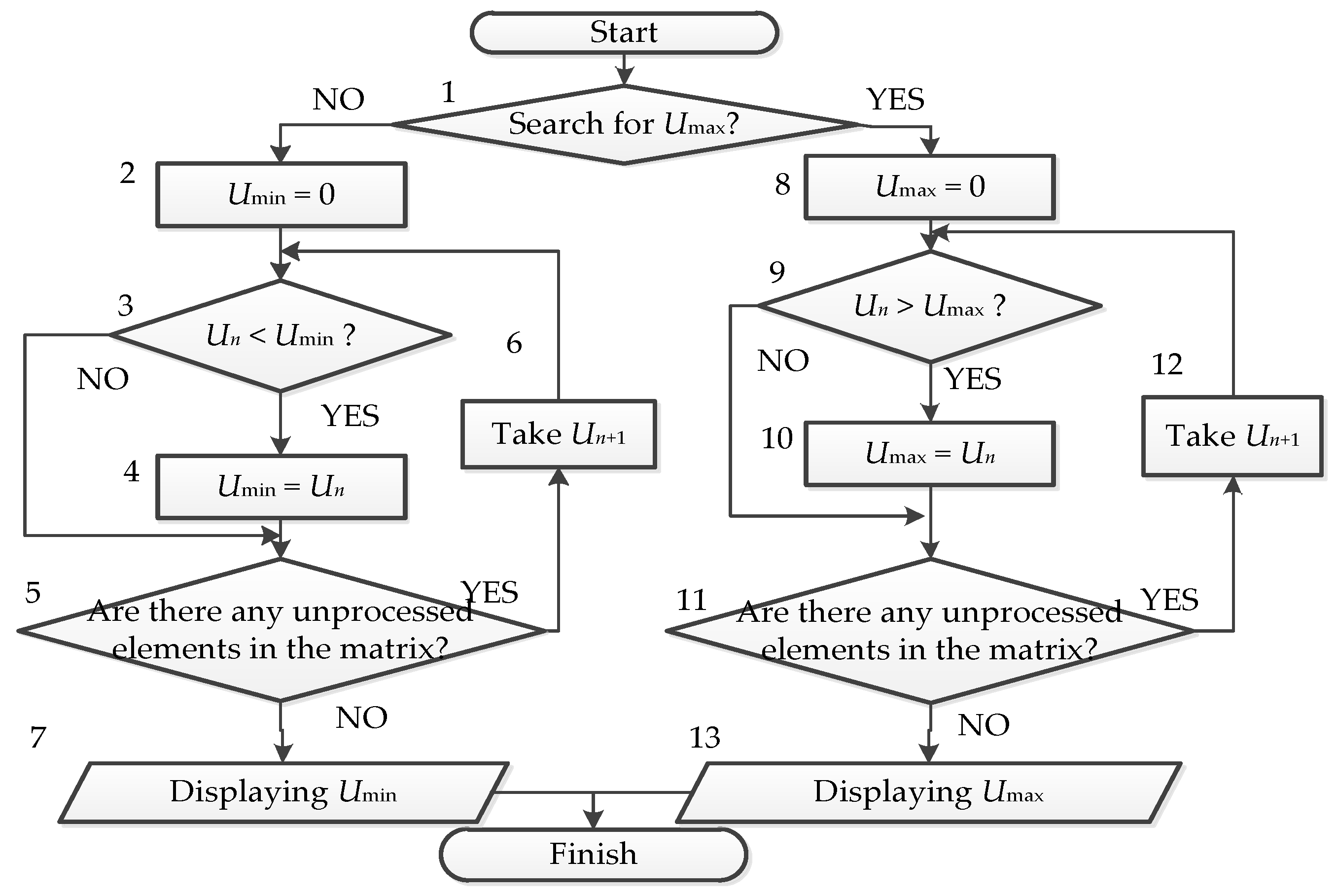
The block diagram of the algorithm for detecting and localizing signal extreme points is shown in Figure 8.
Let us consider this algorithm in detail. The results of calculating the response in one segment are kept in a matrix consisting of one column. The essence of the algorithm is in the blind search for the maximum or the minimum value in the matrix. All symbolic notations in Figure 8 are for voltages, where Umax is the maximum voltage value, Umin is the minimum voltage value, Un is the current matrix element (during the 1st algorithm run n = 1 in the blocks 3 and 9); and n is the number of matrix elements. After the algorithm run, the signal extreme point is displayed. According to the fact that the response is calculated in each segment of each MCTL section, the numbers of the conductor segment and the section (where the signal is localized) are known. The development of this approach resulted in creating an additional program module for TALGAT software [37]. Using this module, ordinary coupled lines were, first, studied and, then, compared with the results of CST MWS software. Then the real PCB bus of a spacecraft ANS was investigated under different conditions.
The computational complexity of the proposed approach involves multiple calculations of a signal waveform. There are as many calculations as segments of an MCTL section multiplied by the number of MCTL sections. We can define a signal waveform calculation with the complexity in Big O notation as O(n2). The complexity of the proposed approach is O(n3).

5. Investigation of Coupled Transmission Lines

5.1. Meander Line with Two Turns

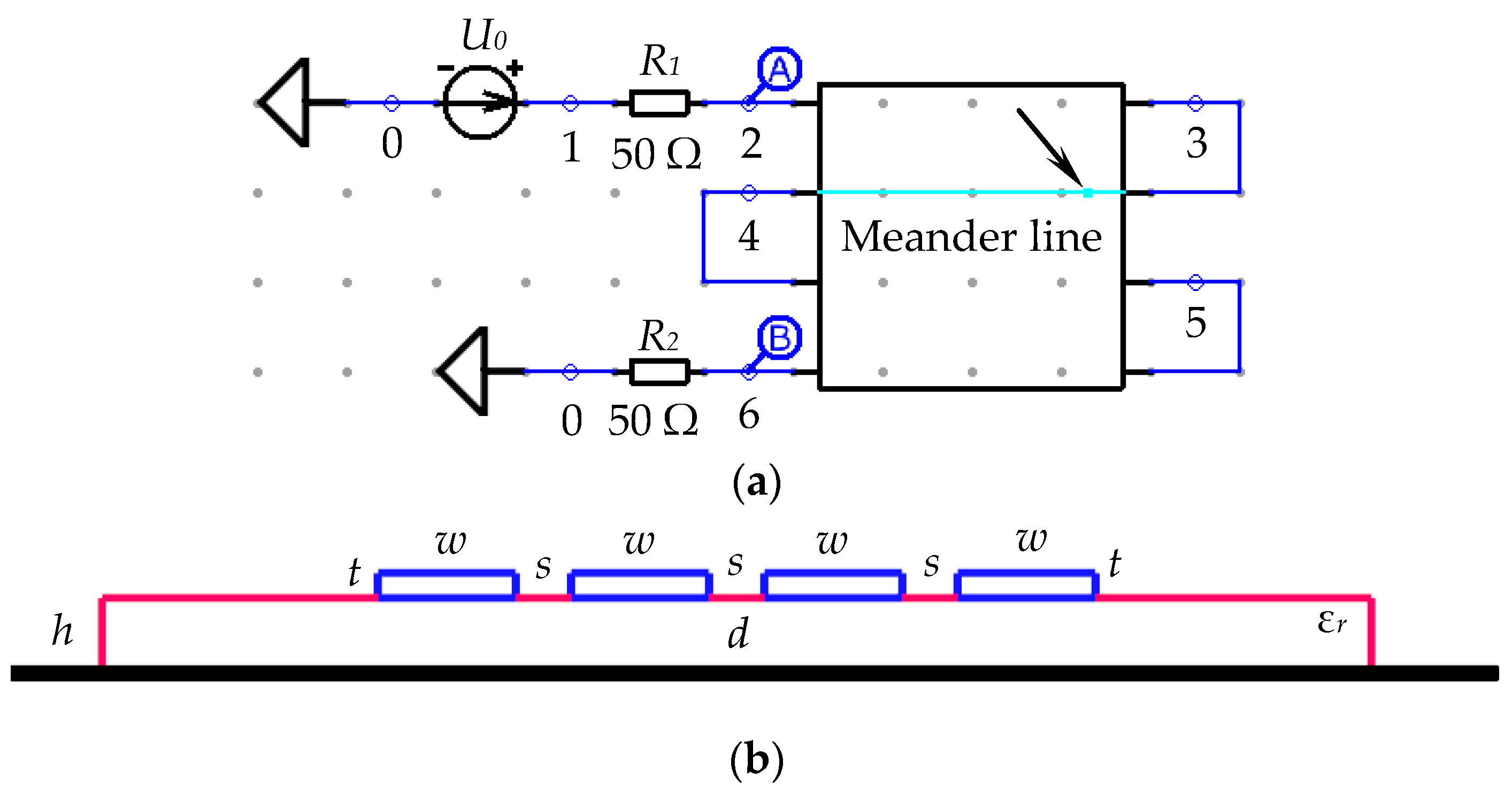
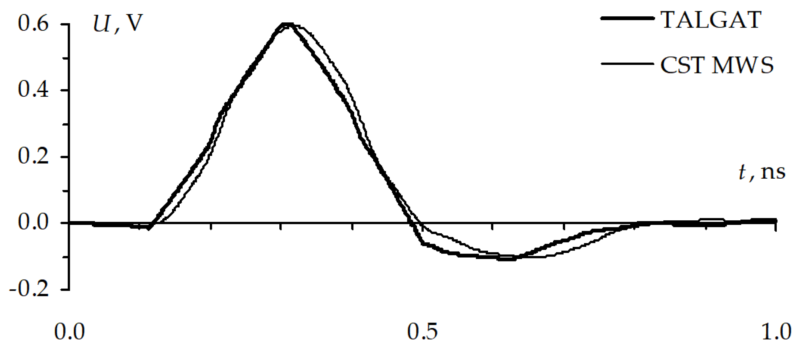
The first structure to be studied was a meander line with two turns [30]. The circuit diagram and the cross section of this line are shown in Figure 9. The length of the line conductors is 27 mm, the conductor width (w) is 0.542 mm, the conductor thickness (t) is 0.1 mm, the dielectric width (d) is 5.149 mm, the dielectric thickness (h) is 0.3 mm, the relative permittivity (εr) is 4.5, and the separation (s) between the conductors is 0.217 mm. The simulation was carried out without losses. Each conductor of the meander line was divided into 50 segments. Therefore, the voltage waveforms were calculated in 200 points along the whole length of the meander line (the MCTL section includes four conductors). The voltage maximum that is 1.14 times higher than the steady-state level was detected and located in segment 46 of the second conductor (shown by the arrow in Figure 9). The waveforms of the localized maximum in comparison with the ones found using CST WMS are presented in Figure 10. A good agreement of the obtained results is observed. The simulation in the CST MWS took 1080 s. while the TALGAT software took 1 s.

5.2. Meander Line with Two Turns

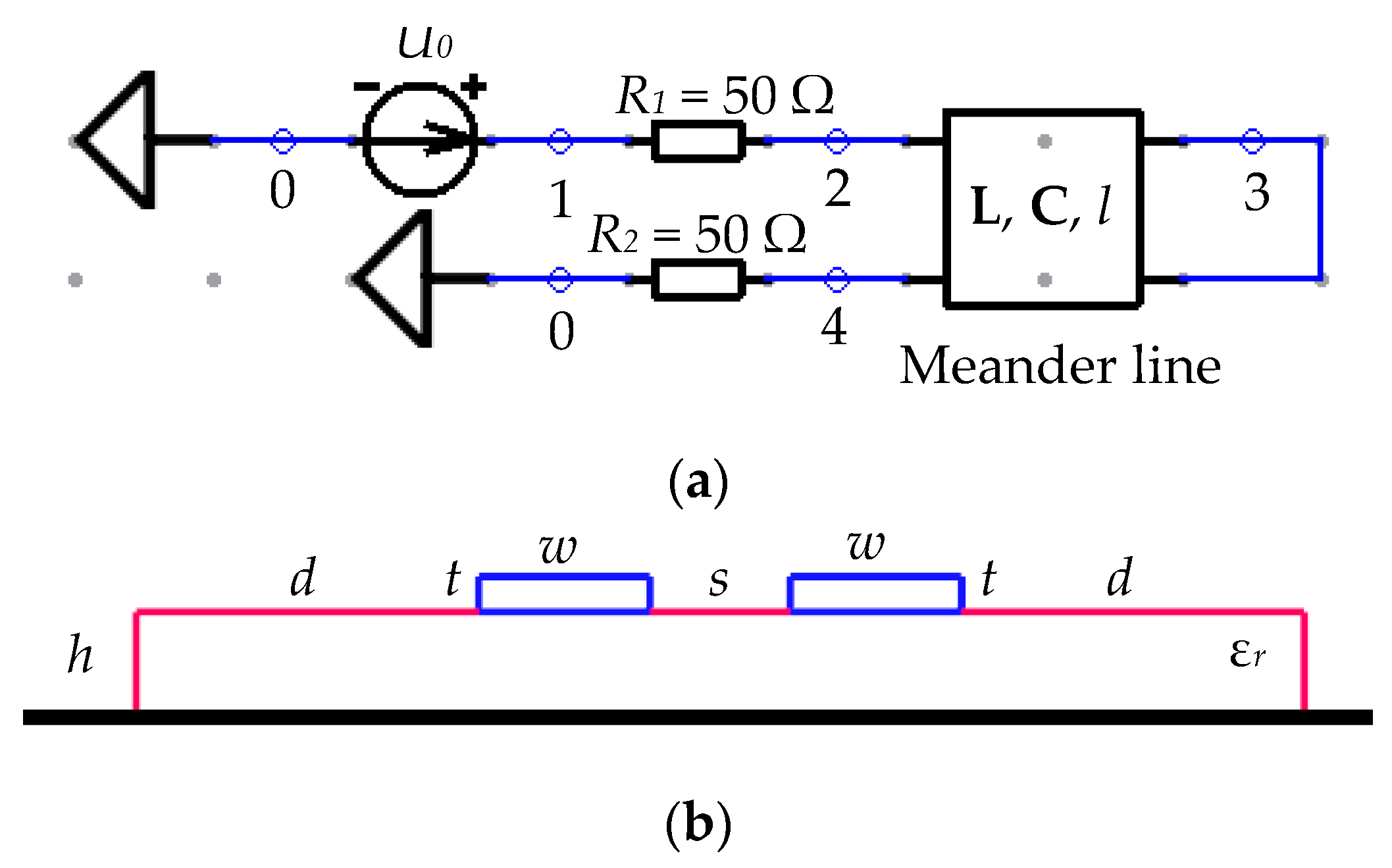
In order to understand the character of voltage transformation better, we investigated a simple meander line with one turn (cross section) [31]. The circuit diagram and the cross section of the line are shown in Figure 11.
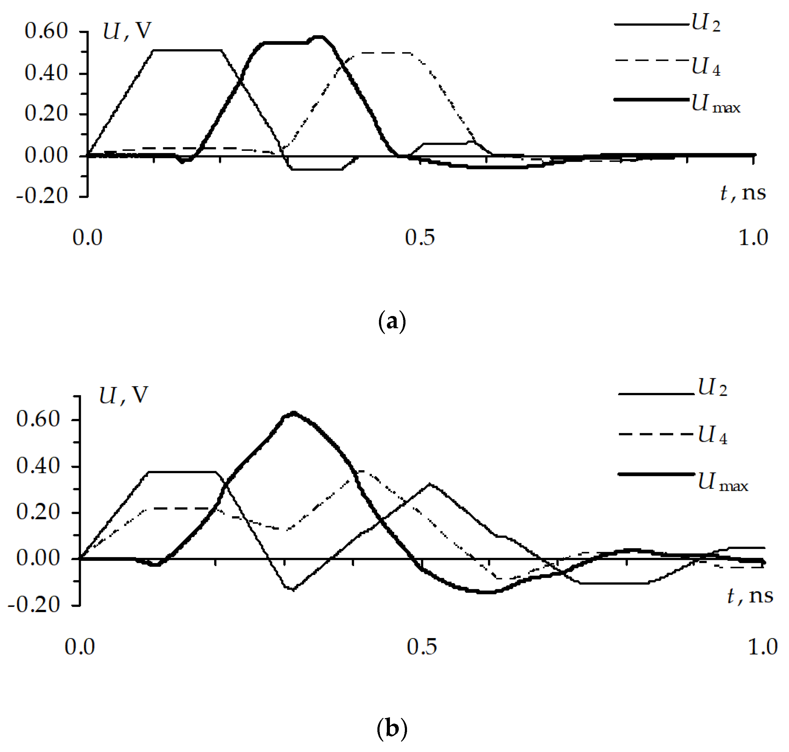
The conductor width (w) is 0.489 mm, the conductor thickness (t) is 0.1 mm, d = 2∙w, the relative permittivity (εr) is 4.5, and the dielectric thickness (h) is 0.3 mm. The aim of the investigation was to calculate signal waveforms with extreme points at different separations (s) (from 0.4 mm down to 1 μm) between the conductors. The different separations were made in order to increase the mutual coupling between the line conductors. The most interesting results of this investigation are presented in Figure 12.
The highest voltage maximum (Umax) was localized with s = 8 μm (Figure 12b). It is twice as high as the voltage amplitude at the input (U2). The comparison of the obtained result with CST MWS is shown in Figure 13. A good agreement of the obtained results is also observed. The simulation in the CST MWS took 840 s while the TALGAT software took 0.5 s.

6. Investigation of Spacecraft ANS PCB Bus

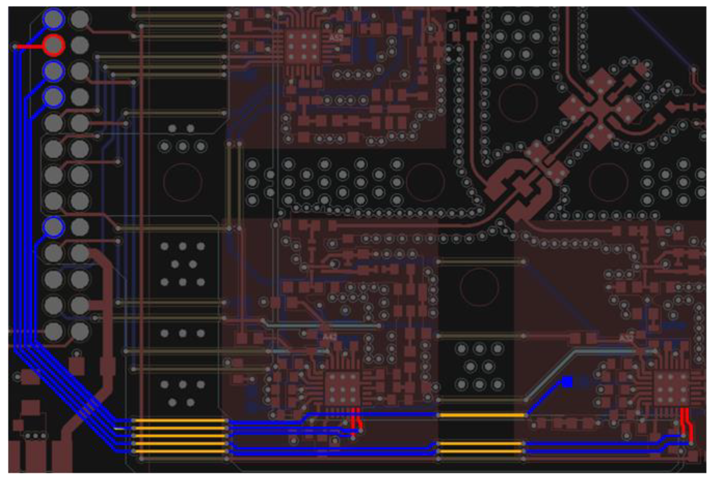
After the study into the simple coupled transmission lines, a complex PCB bus of a spacecraft ANS was simulated then. The PCB bus fragment is shown in Figure 14, and the bus circuit diagram is shown in Figure 15. The resistors of 50 Ohm are connected to the ends of each bus conductors. The conductor bend and via are approximately simulated as the capacitance of 1 pF and inductance of 1 nH, respectively. Each MCTL section cross section is modeled according to the PCB stack parameters. The losses were not taken into account.

6.1. Influence of Ultrashort Pulse Duration on Localization of its Extreme Points in PCB Bus

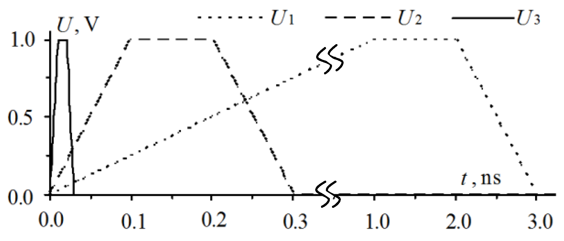
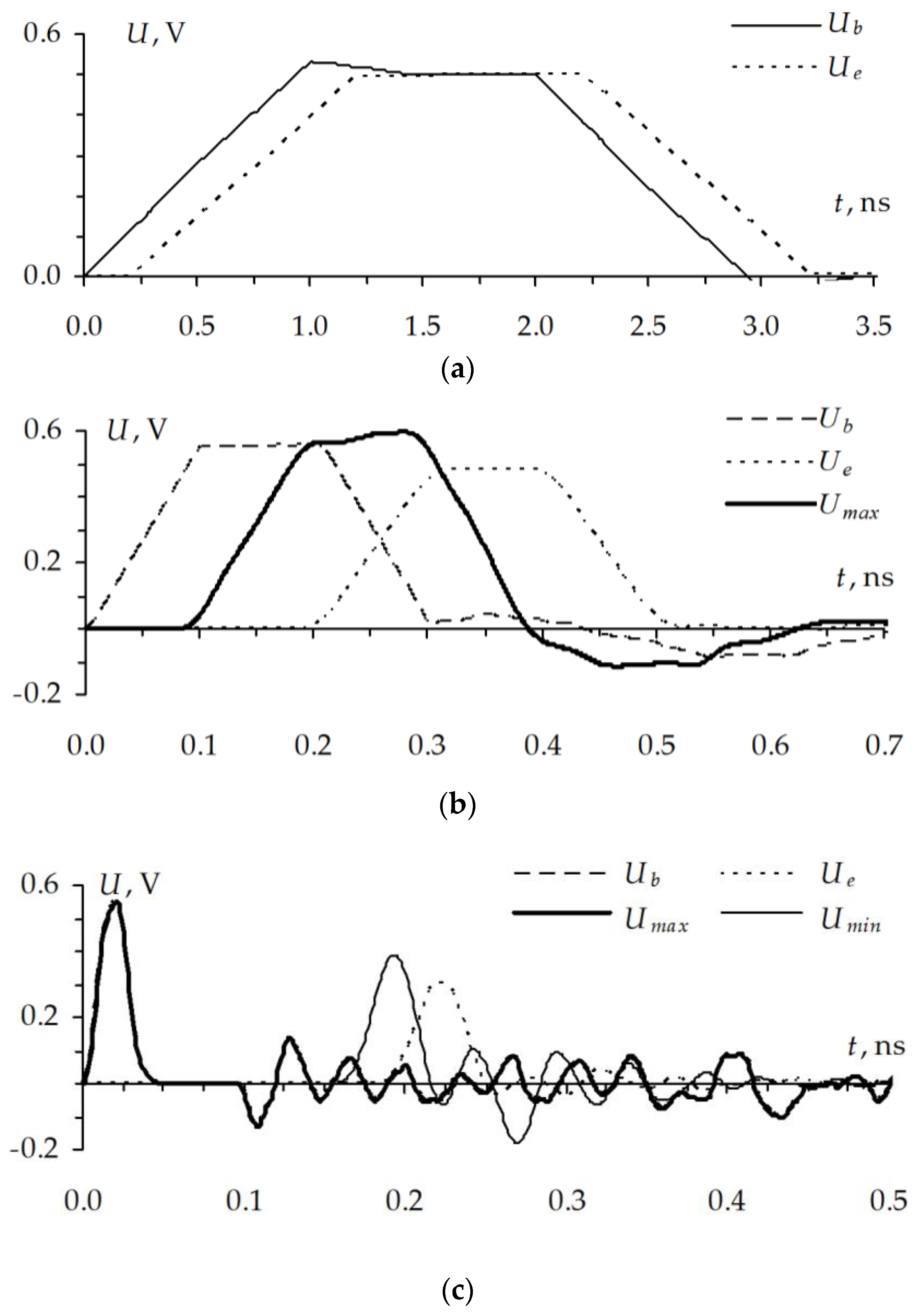
The investigation of the influence of ultrashort pulse duration on the localization of its extreme points in the PCB bus of a spacecraft ANS has been performed in [32]. This paper considers three durations of one ultrashort pulse, each with amplitude of 1 V, as excitations. The waveforms of each pulse are presented in Figure 16. The first pulse (U1) has the rise, top, and fall times of 1 ns, the second (U2) – 100 ps, and the third (U3) – 10 ps, and therefore the whole durations are 3, 0.3, and 0.03 ns. Such choice of excitation parameters is determined by the fact that in such way not only useful signals, but interference ones, are considered.
We determine twenty voltage waveforms in each segment along each conductor of MCTL section, shown in Figure 15, but only the waveforms at the beginning (Ub) and the end (Ue) of the conductor, and the waveforms with the voltage maximum (Umax) and minimum (Umin) values, appearing under each excitation, are presented.
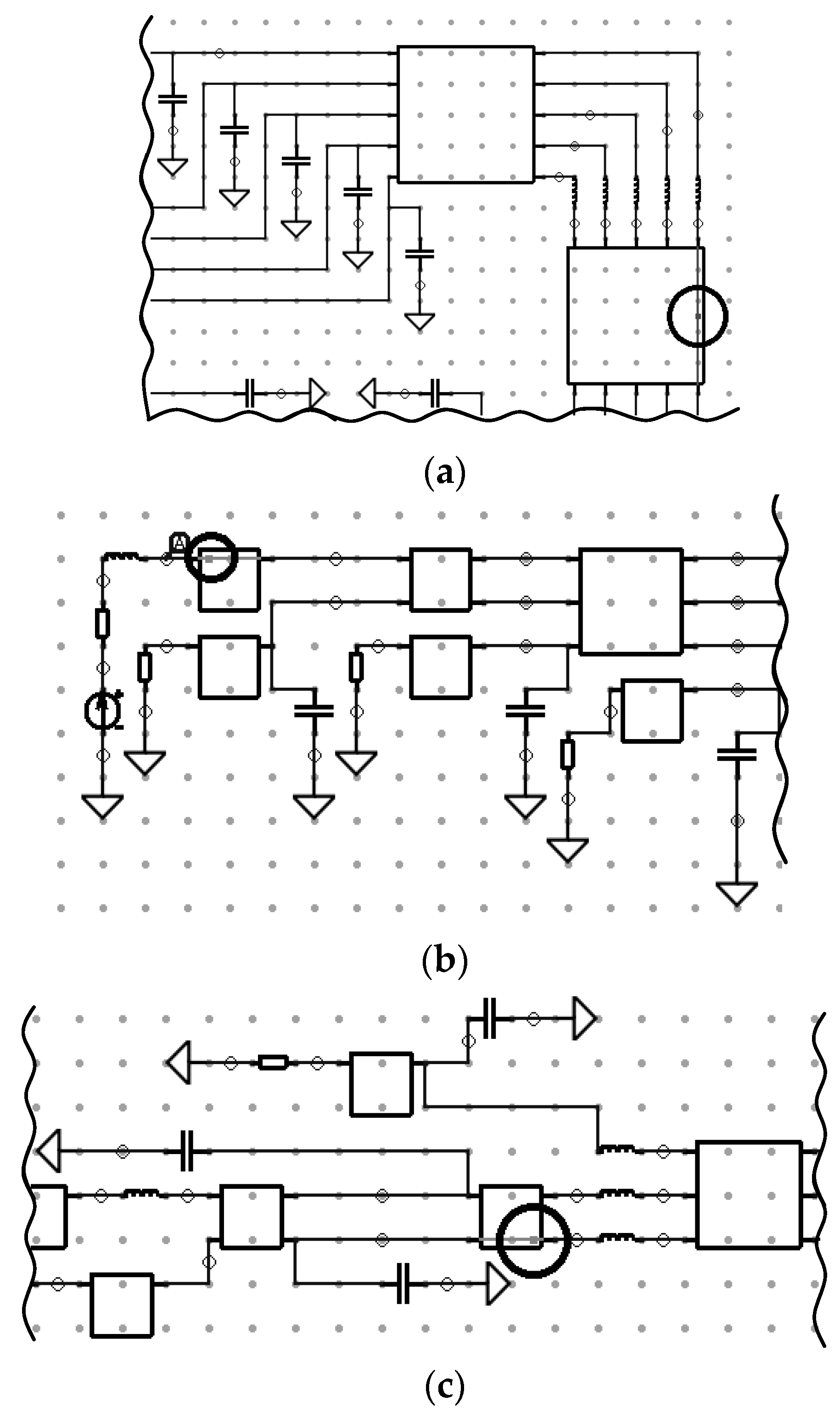
Let us consider the signal waveforms along the active conductor (Figure 17) and the locations of extreme points of these signals, which are shown by circles in Figure 18. We found that the signal maximum coincides with the signal waveform in the node under the excitation U1, and minimums under excitations U1 and U2. By this reason the waveforms of these signals and their locations are not shown in Figure 17 and Figure 18. Table 1 contains the values of the voltage peaks and the numbers of segments with their locations.
Let us consider the excitation (U1). The extreme points of the waveforms presented in Figure 17a and their location coincide with the waveforms at the conductor’s ends. Let us consider the U2 and U3 excitations which can be relegated to high-speed or interfering signals because their durations are shorter. Under the U2 excitation, voltage maximum is 0.59 V (Figure 17b) which is 18% higher than the steady-state level of 0.5 V. The maximum is localized in segment 10 (Table I) in one of the transmission line sections with five conductors that are located on another layer (Figure 18a). Under the U3 excitation, not only the voltage maximum of 0.552 V that exceeds the 0.5 V level by 10% is detected, but also a minimum of minus 0.18 V (Figure 17c) or minus 36% of 0.5 V, which is lower than the level of zero. Moreover, it is shown in Table 1 and Figure 18b,c that the extreme points are localized in absolutely different places.
Let us consider the results for the U3 excitation. Besides the appearance of peak values, it was found that there appeared multiple reflections and the signal amplitude at the output of the line decreased. It was 0.4 V in Figure 17c, which is 20% lower than the 0.5 V level. The investigation shows specific aspects of detecting and localizing extreme points of the ultrashort pulse with various durations. For example, the highest maximum value (about 0.6 V) is detected under the U2 excitation as we can see from Table 1. The extreme points are located in different transmission line sections and segments along these conductors (i.e., in different places of the PCB).

6.2. Influence of Ultrashort Pulse Duration on Localization of Crosstalk Extreme Points in PCB Bus

The investigation of the influence of ultrashort pulse duration on the localization of crosstalk extreme points in a PCB bus of a spacecraft ANS has been performed by [33]. This study used four generators and conductor 3 (central) was passive (Figure 19). In this figure, the arrows show the generators, and the conductors are numbered. The same durations of the ultrashort pulse (shown in Figure 16) were used as excitations. The simulation results for conductor 3 (central) are shown in Figure 20 and the segments with peak voltage values are pointed in Figure 21.
The voltage extreme points and its location segment numbers are shown in Table 2. Consider the excitation of the useful signal (U1). The signal waveforms calculated for conductor 3 are presented in Figure 20a, but their extremes and location are similar to the waveforms calculated at the ends of the conductor. Let us consider the excitations U2 and U3 which can be regarded as interference signals. These excitations have the shorter durations than the useful ones. Some voltage maximums are detected, but they are located in the diagram nodes. The voltage minimum calculated under the excitation U2 is minus 0.126 V (25.2% of 0.5 V). The location of this extreme point is in the segment 5. But the voltage minimum calculated under the excitation U3 is minus 0.199 V (39.8% of 0.5 V) and is located in segment 8.
This study unveils the specific details of detecting and localizing extreme points for an ultrashort pulse with different durations. The highest maximum value (0.145 V, 29% of 0.5 V) appears under the excitation U3 as it shown in Table 1 (the full duration of the pulse was 0.03 ns). The highest minimum value (minus 0.199 V, 39.8% of 0.5 V) is also under the excitation U3. Considering that the maximum acceptable crosstalk level in the ANS PCB bus should be less than 10% of signal amplitude in the active conductor, it follows that all detected extreme points (excluding those under the excitation U1) dissatisfy this condition.

6.3. Simulation of ESD Effects on PCB Bus

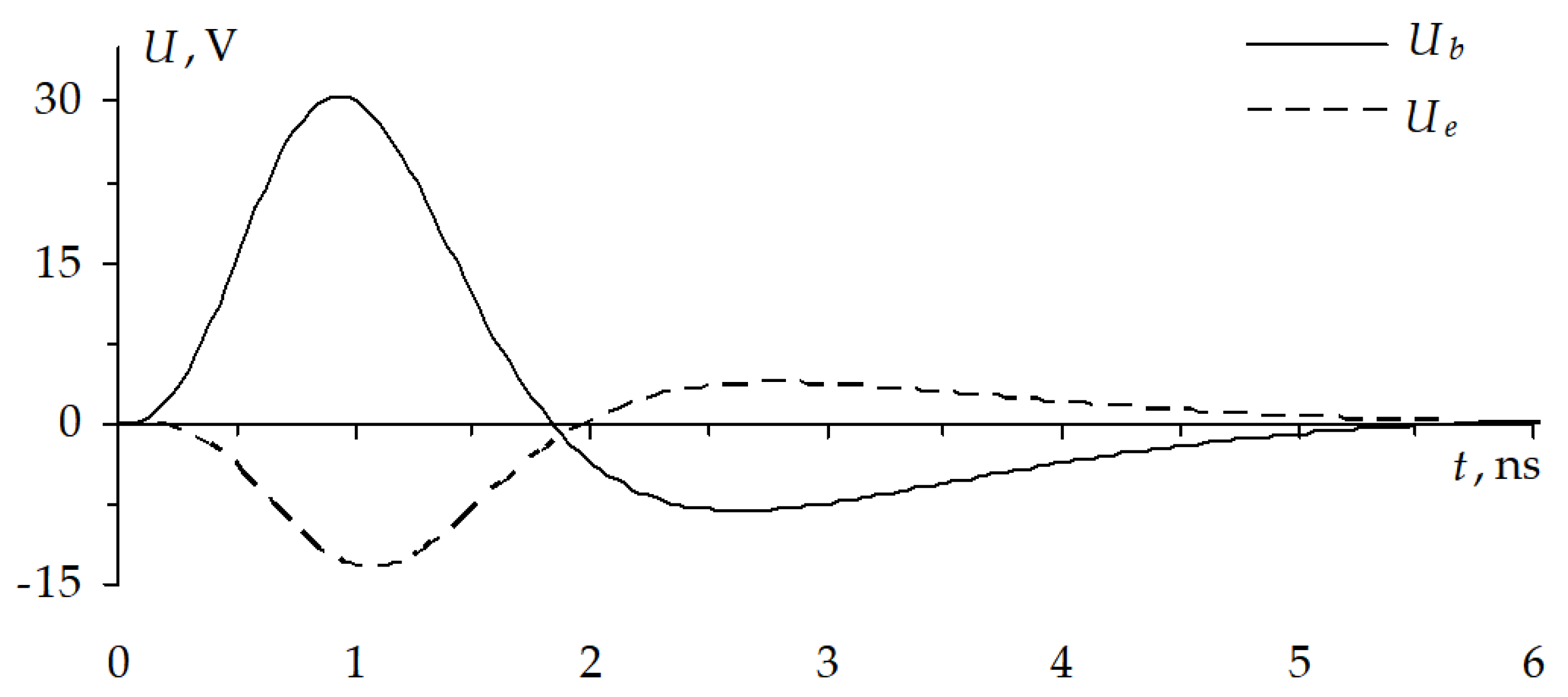
The simulation of ESD effects on a PCB bus of a spacecraft ANS have been described in [38]. The ESD, whose parameters and selection justification are described in [39], was chosen as excitation. The current waveform according to the IEC 61000-4-2 [40] standard was used. It was excited on each conductor in turns and the voltage waveforms were calculated along each conductor. In addition, the case was considered when all conductors, except the central one, were under the ESD excitation. The results of the last case are presented further. The simulation results for the central conductor when the four conductors were active and the central one was passive are presented in Figure 22.
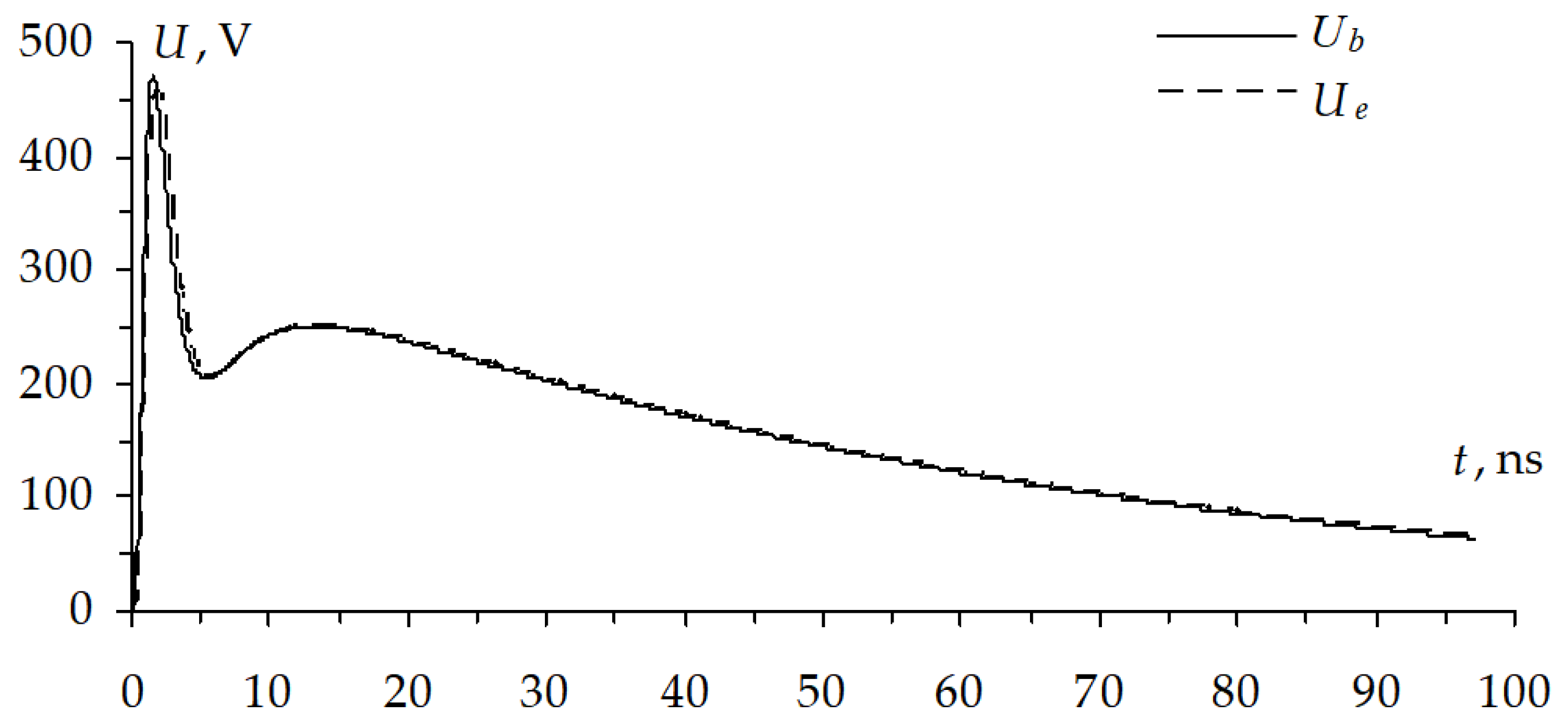
The waveforms calculated at the beginning of one of the active conductors are shown in Figure 23, (waveforms for others are almost the same).
Let us consider the signal waveforms in the active conductor 1. The voltage amplitude of 470 V, which is rather dangerous for integrated circuits (IC), is observed in this conductor (Figure 23). The extreme points coincide with the voltages at the input or the end of the conductor, and therefore they are not shown in the figures. Let us consider the signal waveforms in the passive conductor (Figure 22). The crosstalk amplitude is 32 V which is 6.8% of the signal level in the active conductors. The significant negative voltage (minus 14 V) is also observed.
This work demonstrates the importance of studying the ANS PCB bus under ESD excitation, and therefore the simulation of ESD excitation on several bus conductors at once has also been carried out. First of all, it showed that considerable peak voltages along the investigated bus conductors (higher than the voltages at the ends of the conductors) did not appear under the ESD excitation (in contrast to the ultrashort pulse [32,34,41]).
Another important finding was that the voltage amplitude in the active conductor can be near 0.5 kV and could disable an integrated circuit (IC). The crosstalk can also be dangerous because it can be deemed in many circuits as the useful signal (1–2 ns, 32 V) and become the reason for IC upset. Moreover, we should note that these results were obtained for the resistances of 50 Ohm while the high input impedance of a real IC can double these values. Such amplitudes can strongly influence the operation of radio-electronic equipment of critical significance.

7. Optimization by Genetic Algorithms

In the following investigations, we have used the optimization by genetic algorithms in various options.

7.1. Optimization of Ultrashort Pulse Duration by Criteria of Peak Voltage Maximization in PCB Bus

The simple binary-coded GA (a number of bits for each parameter is taken 16 as default in TALGAT software) was launched with the following parameters [34]: coefficient of mutation was 0.1 and coefficient of crossover was 0.5. The rise, flat top, and fall durations were separately optimized so the total duration range was from 1 ns to 10 ps (as shown in Figure 16), the number of chromosomes was three and five, and the number of populations was five, 25, 50, and 75. The sum of peak voltages from the ends of the PCB bus conductors 1, 3, and 5 was maximized (these points are considered as examples of the critical places where the bus conductors are connected to the other PCB components). The aim of the second part of the investigation was to define the rise, flat top, and fall duration values of the ultrashort pulse, at which the sum of voltages in the preset points will be maximal.
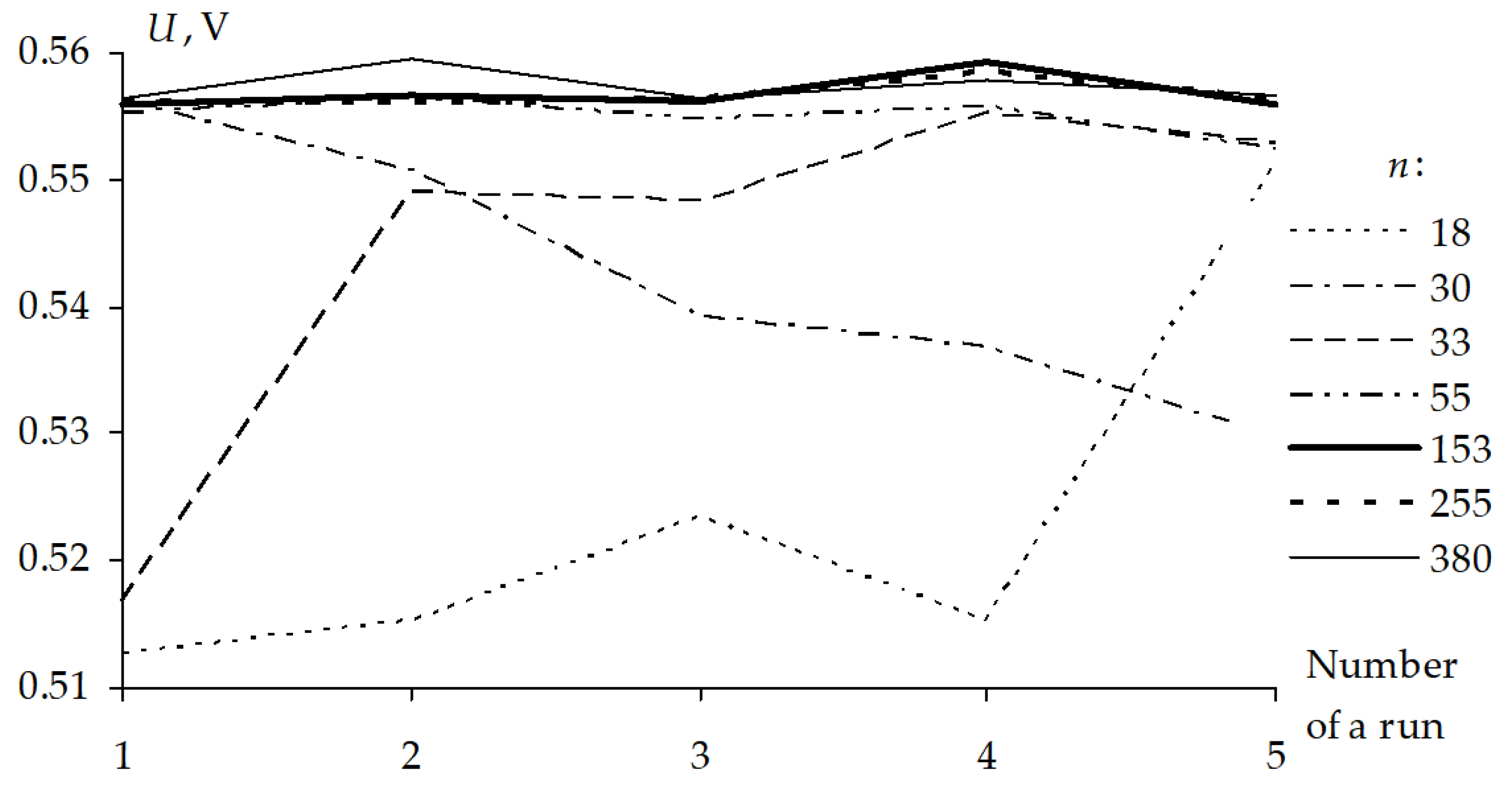
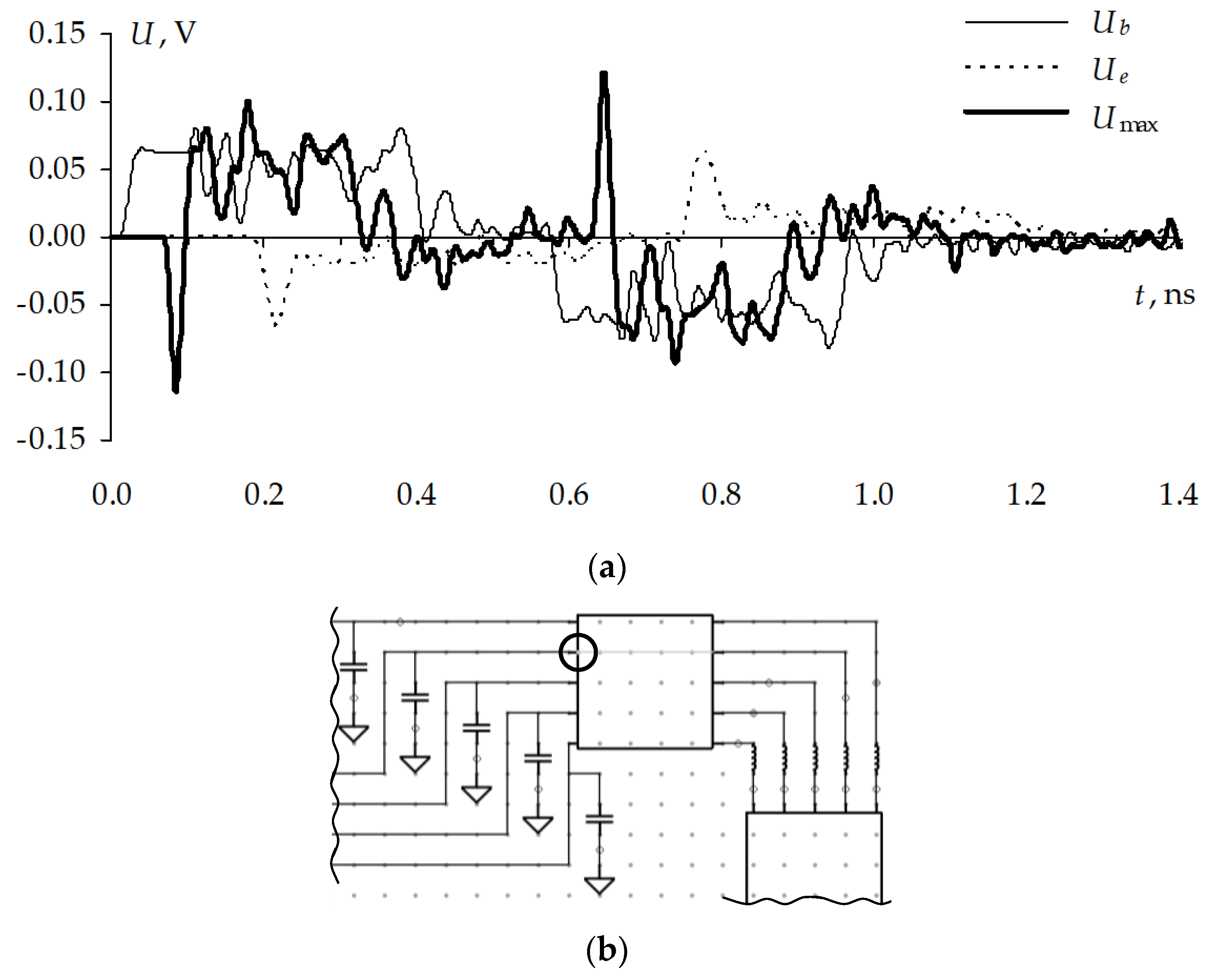
The results of the GA run, including the calculation of time, (t), for the rise, flat top and fall times of the ultrashort pulse are presented in Table 3 (the number of chromosomes is five). The GA was launched five times for each combination of the population number (NP). This is caused by the necessity to check the convergence of the fitness function results. The diagram of convergence of the Umax values with a different number (n) of fitness function (product of the number of chromosomes and the number of populations) calculations is shown in Figure 24. A total of 20 voltage waveforms were calculated in each segment along each conductor of each MCTL section from Figure 15 with the obtained results for the highest fitness function value (run 2 from Table 3, when the number of populations was 75), but only the waveforms at the beginning (Ub) and end (Ue) of the conductor and also the waveforms with the voltage maximum (Umax) values are presented. The results are presented only for one active and one passive conductor with the highest crosstalk amplitude.
The voltage waveforms calculated along the active conductor are presented in Figure 25a, and the location of the ultrashort pulse maximum is shown in Figure 25b. The voltage waveforms along the passive conductor are shown in Figure 26a, and the crosstalk maximum location is shown in Figure 26b. Let us consider the optimization results. With the maximal number of calculations, the fitness function value is 0.55459 V (Table 3) and the average (of five runs) calculation time is 5767.5 s. The fitness function results show a good convergence when the numbers of calculations are 255 and 380, the results differ only in the third decimal place. The voltage maximum in the active conductor is detected and localized with the optimized parameters (short rise and fall times, and maximal flat top duration) which are obtained at run 2 (the number of chromosomes is five and the number of populations is 75) from Table 3. The detected voltage maximum is 0.68 V (Figure 25a) which is 36% higher than the steady state level. The maximum is located in segment 6 (Figure 25b) in an MCTL section of another layer of the PCB.
Moreover, the crosstalk maximum is detected and localized in segment 1 in one of the five conductor transmission line sections. The crosstalk maximum is 0.12 V which is 24% of a steady-state level. The investigation shows the importance of the GA for optimization for detecting and localizing signal peak values or the sum of several signals under excitation of the ultrashort pulse with different durations.

7.2. Optimization of Ultrashort Pulse Duration by Criteria of Peak Voltage Maximization in PCB Bus

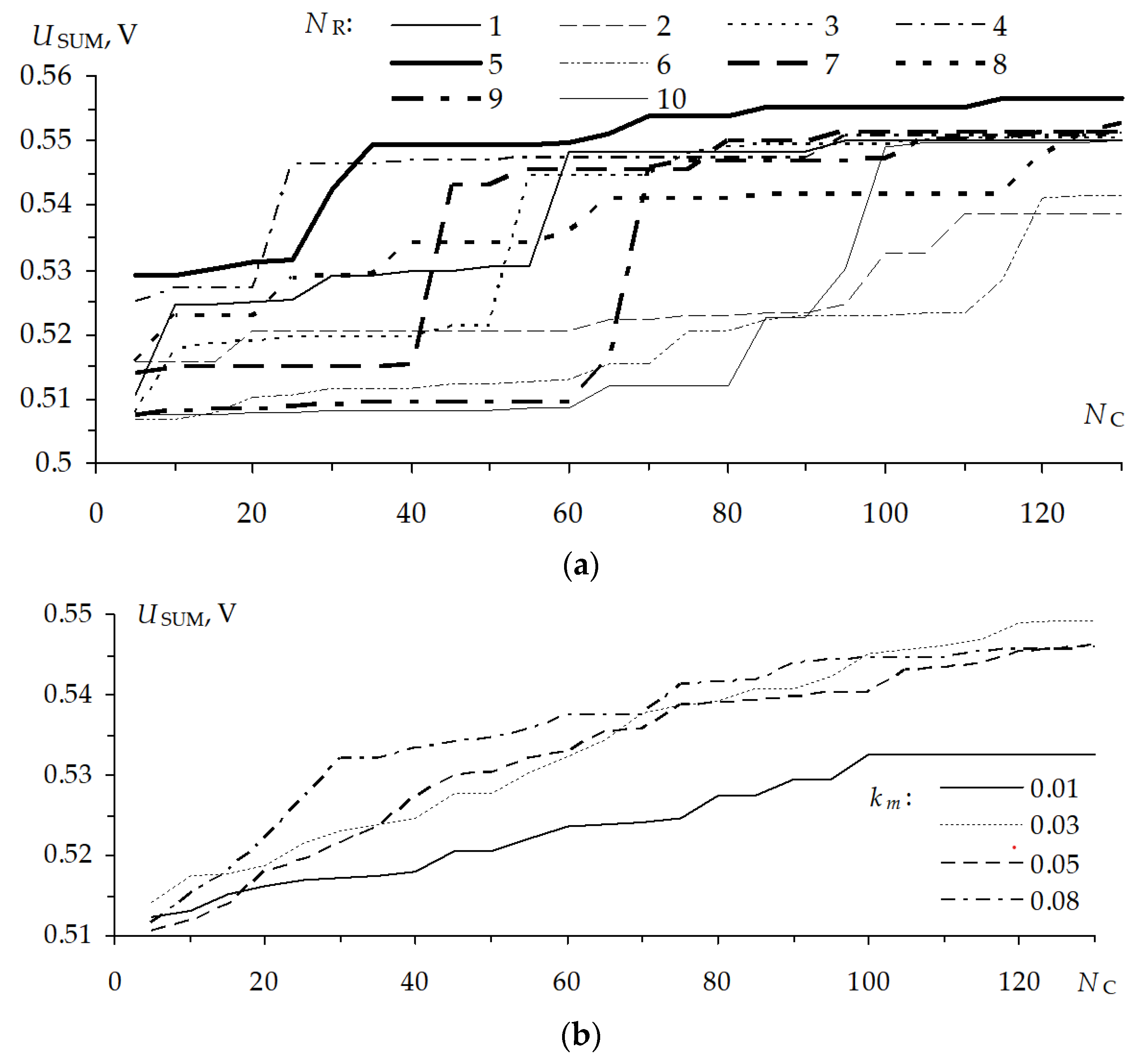
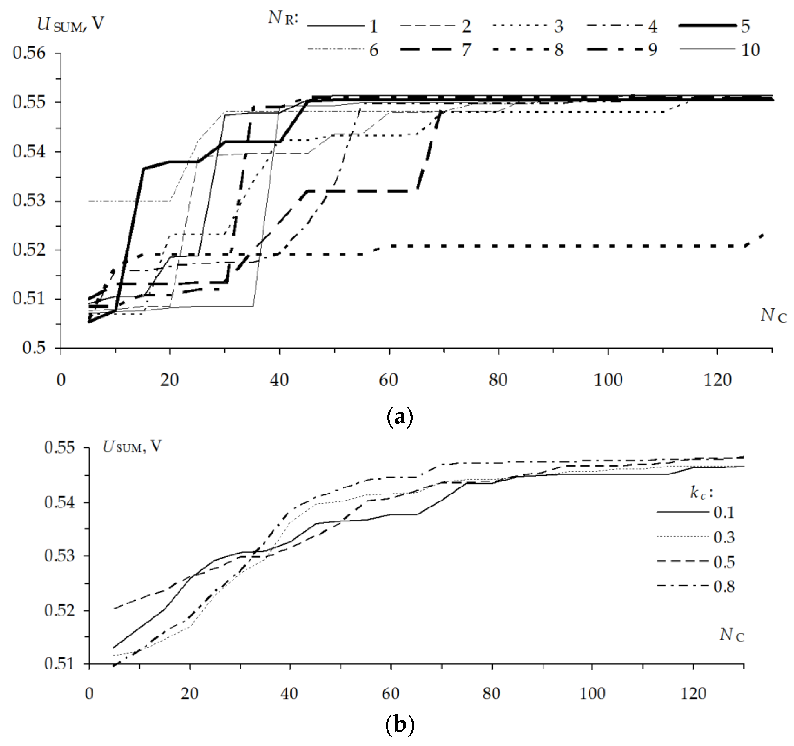
The investigation focused on the influence of crossover and mutation coefficients on the GA for optimization of the ultrashort pulse duration by criteria of peak voltage maximization in the PCB bus [35] and employed a simple binary-coded GA. The investigation consisted of two parts. In the first part, the mutation coefficient (km) ranged from 0.01 up to 0.08, and, in the second part, the crossover coefficient (kc) ranged from 0.1 up to 0.8. In the first part, kc = 0.5 and,, in the second part km = 0.1. Three parameters, tr, td, and tf, were optimized in the range from 1 ns down to 0.01 ns when the chromosome number was five and the number of populations was 26 (so the total GA calculation number was 130). The sum of peak voltages at the ends of the PCB bus conductors 1, 3, and 5 was maximized. The aim of the optimization was to define the rise, flat top, and fall duration values of the ultrashort pulse, at which the sum of voltages (USUM) in the preset points will be maximal. It is important to notice that it is necessary to choose a greater number of GA calculations to provide a more complete investigation. The simulation of excitation by several sources is also useful, but due to the fact that the work presents the preliminary stage of the investigation only, it was decided to choose a small number of calculations and one source only. The values of the sum of maximum voltages in the preset points for the first part of the investigation are presented in Table 4. The presented results are obtained with kc = 0.1 and different km for ten GA runs.
The convergence diagrams for the best fitness function results obtained by different runs are shown in Figure 27a, where NC is the calculation number and NR is the run number. The presented results are obtained when km = 0.03 because with such km the Umax in Table 4 is the highest. Convergence diagrams of the arithmetic average of ten runs with different km are shown in Figure 27b. The GA run results of the second part of the investigation (the sum of maximum voltages at I, II, and III points when km = 0.1 and kc is different) are presented in Table 4.
The convergence diagrams for the best fitness function results obtained at different runs are shown in Figure 28a. The presented results are obtained when kc table= 0.8 because with such kc the Umax in Table 3 is the highest. The convergence diagrams of the arithmetic average of ten runs with different kc are shown in Figure 28b. As regards the best fitness function result, all obtained values are similar and differ in the third decimal place. Additionally, the highest result (0.55704 V) is obtained with km = 0.03 (Table 4). Let us consider the results of the second part of the investigation. As regards the best fitness function result, the situation is the same as for the first part of the investigation, all obtained results are similar and differ in the third decimal place only. Meanwhile, the highest result is 0.55448 V (obtained with kc = 0.8).
The investigation shows the importance of the GA for optimization of the sum of several signals under excitation of the ultrashort pulse with different durations. For instance, as we can see from Table 4 and Table 5, when we change either mutation or crossover coefficients, the highest fitness function is near 0.55 V and 0.55132 V in Table 4, and 0.55173 V in Table 5. It is found that the mutation coefficient variation strongly influences the convergence of results. Indeed, changing the mutation coefficient results in convergence deceleration and the diagrams are observed to stand out. The crossover coefficient variation gives us the fastest convergence (with kc = 0.8 it is at the 70th calculation). However, these coefficient variations hardly influence the detected peak voltages of the ultrashort pulse and crosstalk. The obtained peak voltages have the same amplitudes.

7.3. Optimization of PCB Bus Loads by Criteria of Peak Voltage Minimization

The investigation involved a GA for optimization of the PCB bus loads by criteria of peak voltage minimization [41]. The GA with binary encoding was launched with the following parameters: the coefficient of mutation = 0.1 and the coefficient of crossover = 0.5. During the optimization ten variables (resistances) were chosen which changed in the range from 1 to 200Ω. The number of chromosomes was three, five, seven, and 10, and the number of populations was six, eight, 11, and 26. It was minimixed the maximum sum of the peak voltage values at preset points of the ANS PCB bus (outputs of the conductor 1, 2, and 3). Therefore, the aim of the optimization was to determine such resistance parameters, at which the sum of the highest voltages at points I, II, and III will be minimal.
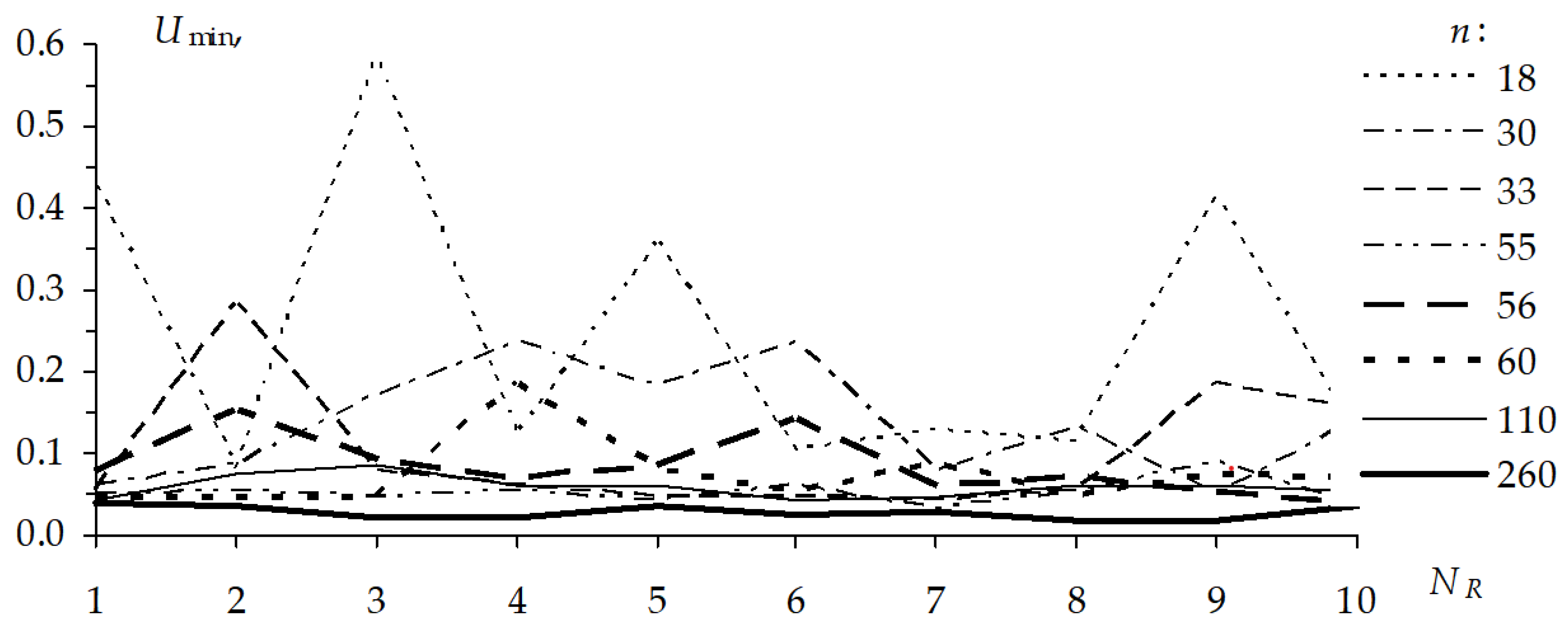
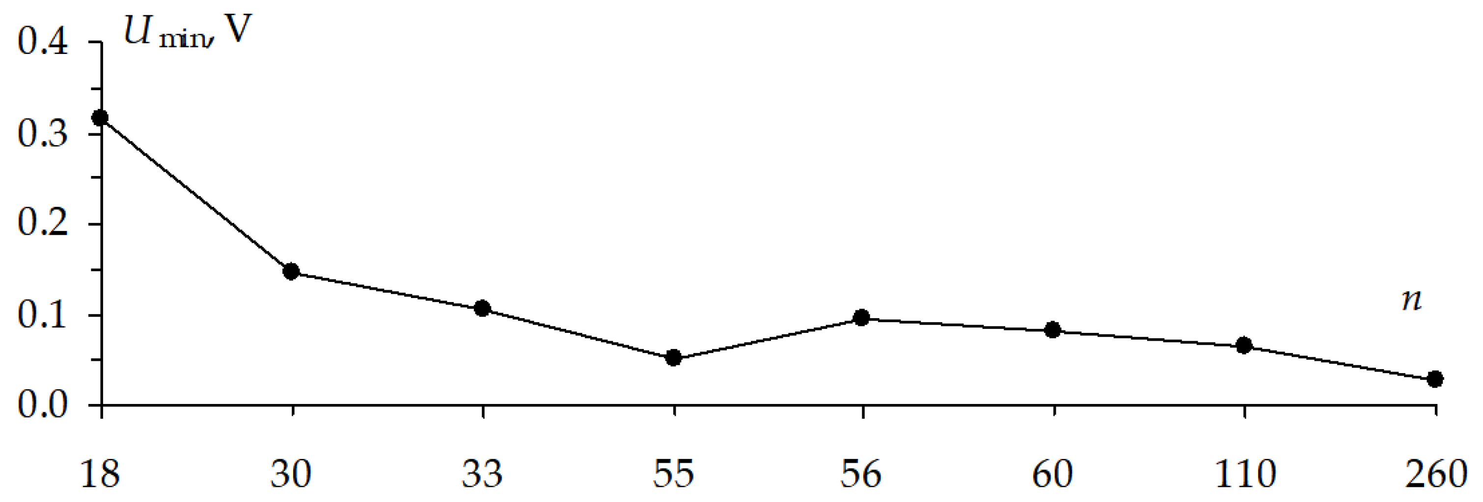
The GA optimization results (Umin, the minimum value of the sum of peak voltages at points I, II, and III) with different runs and the number of the fitness function calculations are presented in Table 6, where NR is a number of a run, and n is the number of fitness function calculations. The GA was launched ten times for each combination of the chromosome number and the population number. It was made in order to check the convergence of the fitness function results. The convergence diagram of the Umin values with a different n is shown in Figure 29. The dependences of the minimum voltage values on the n are shown in Figure 30.
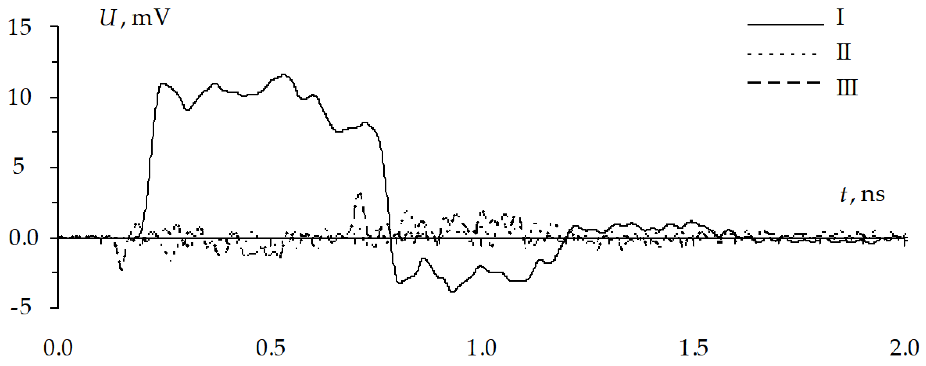
The resistance values, obtained for the best fitness function result (run 9 from Table 6 when n was 260), were used for calculating voltage waveforms. The waveform was calculated at the preset points with the use of these parameters (Figure 31). In addition, Figure 32 shows the voltage waveforms which are calculated in these points before the optimization.
Consider the results of the optimization from Table 6. The result of the fitness function becomes smaller with an increase in the number of calculations (it is also shown in Figure 30). It is observed that a good convergence in the fitness function results when the number of calculations is more than 110 (Figure 29). With the maximal number of calculations, the summarized peak voltage value is 16 mV (run 9 from Table 6) which is 30 times smaller than the signal amplitude (0.5 V) in the active conductor before using the optimization (Figure 32).
The significance of the optimization by means of GA to detect and localize the sum of several extreme points of a signal with a changing of load parameters is shown in this study. For example, the use of optimization helps to decrease the sum of extreme points by 30 times.

8. Use of Evolution Strategies

However, despite the popularity of GAs in various scientific spheres, other optimization methods are also used [42]. Therefore, it is useful to consider how the task of detecting and localizing the signal extreme points in an ANS PCB bus can be solved by an another method of optimization, for example, an evolution strategy (ES). The ESs have a parameter of initial solution (IS) in contrast to GAs, and it is useful to study the effect of the IS of ESs on the signal extreme point in a preset point of the ANS PCB bus when detecting the worst-case effects.
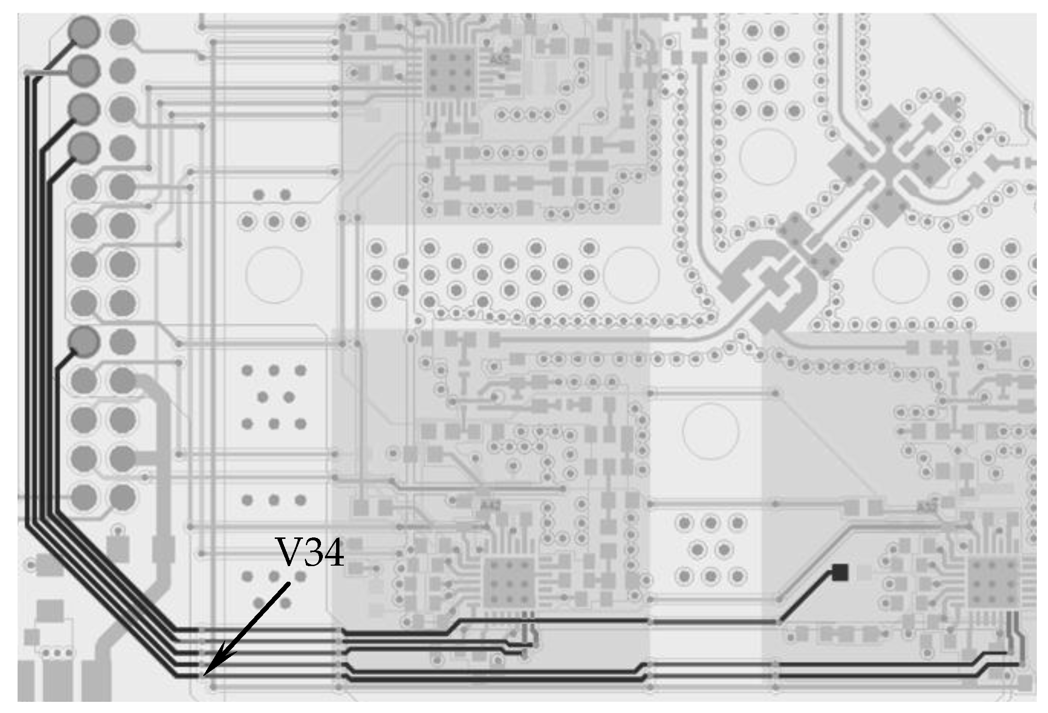
The goal of this study is to investigate the use of an ES and the IS influence when detecting the worst-case effects of the ultrashort pulse propagation in the PCB bus of a spacecraft ANS. The PCB fragment with the preset point is shown in Figure 33.
The ES algorithm in general view can be formulated as [43]:
(1)
The initialization of a population P μ = { a 1 , …, a μ } with the use of μ parent chromosomes.
(2)
The generation of λ offspring a ^ forming the offspring population P ^ λ = { a ^ 1 , …, a ^ λ } where each offspring a ^ is generated by the following steps:
(3)
Select (randomly) ρ parents from Pμ (if ρ = μ take all parental individuals instead).
(4)
Recombine the ρ selected parents to form a recombinant individual r.
(5)
Mutate the strategy parameter set s of the recombinant r.
(6)
Mutate the objective parameter set, y, of the recombinant, r, using the mutated strategy parameter set to control the statistical properties of the object parameter mutation.
(7)
The selection of a new parent population (using deterministic truncation selection) from either the offspring population P ^ λ (this is referred to as comma-selection, usually denoted as “(μ, λ) selection”), or the offspring P ^ λ and parent Pμ population (this is referred to as plus-selection, usually denoted as “(μ + λ) selection”).
(8)
Go to 2 until the termination criterion is fulfilled.
The barecmaes2.py module [43] was used with TALGAT software to perform optimization. The optimization was applied to the whole ultrashort pulse in order to get the highest extreme value of the voltage in the V34 node (shown in Figure 33). The sigma of the ES algorithm was 10 ps. The ES was launched ten times for each IS (3 ns, 300 ps, and 30 ps). The goal of the optimization was to get such duration values of the ultrashoprt pulse at which the extreme value of the voltage in the V34 node would be the highest.
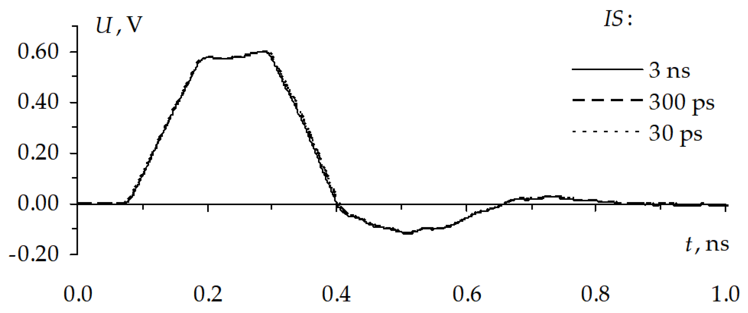
The results of the ES operation are the following: the peak voltages (Umax) in the preset point (for ten ES runs) and the best solutions with different ISs of the ES are shown in Table 7. (Cells with the highest Umax for each IS are colored in yellow.) The signal waveforms calculated with IS = 3, 0.3, 0.03 ns for the highest Umax are shown in Figure 34.
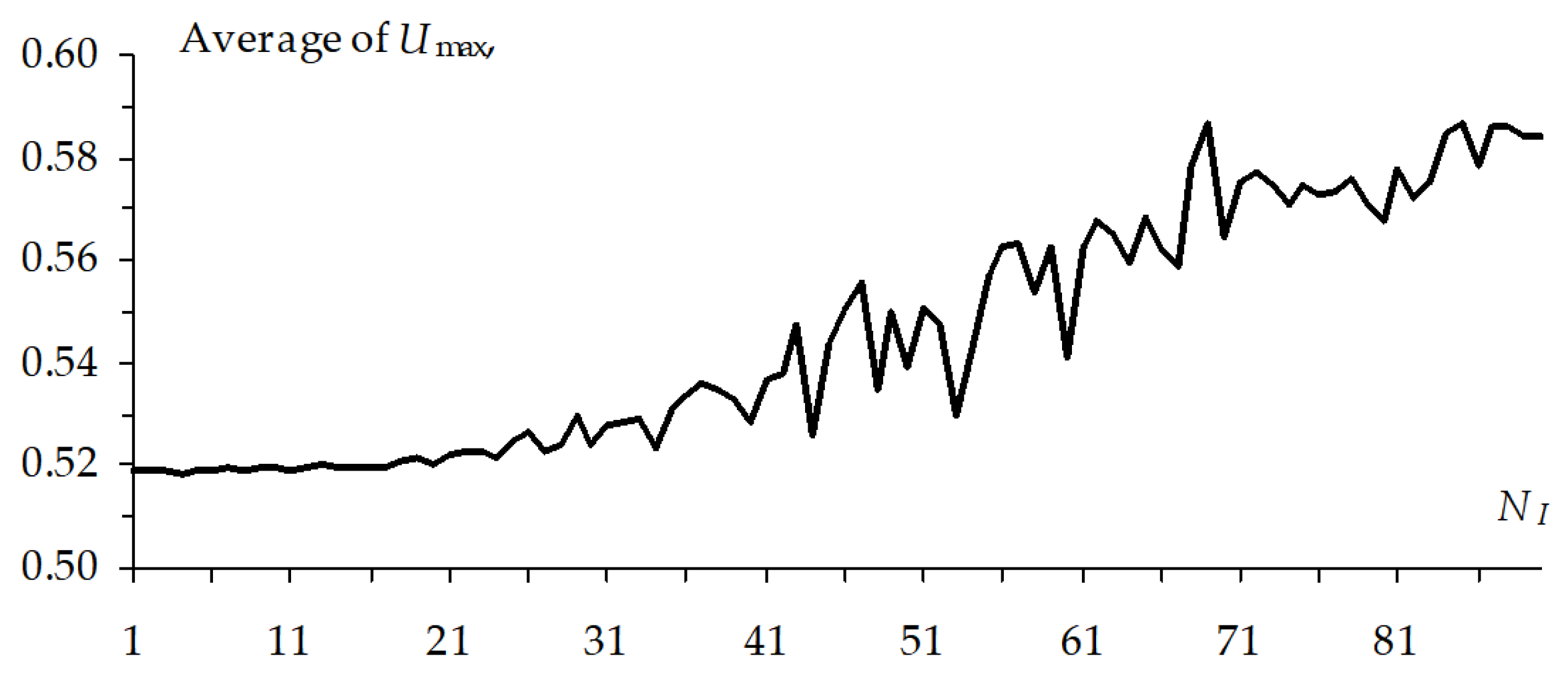
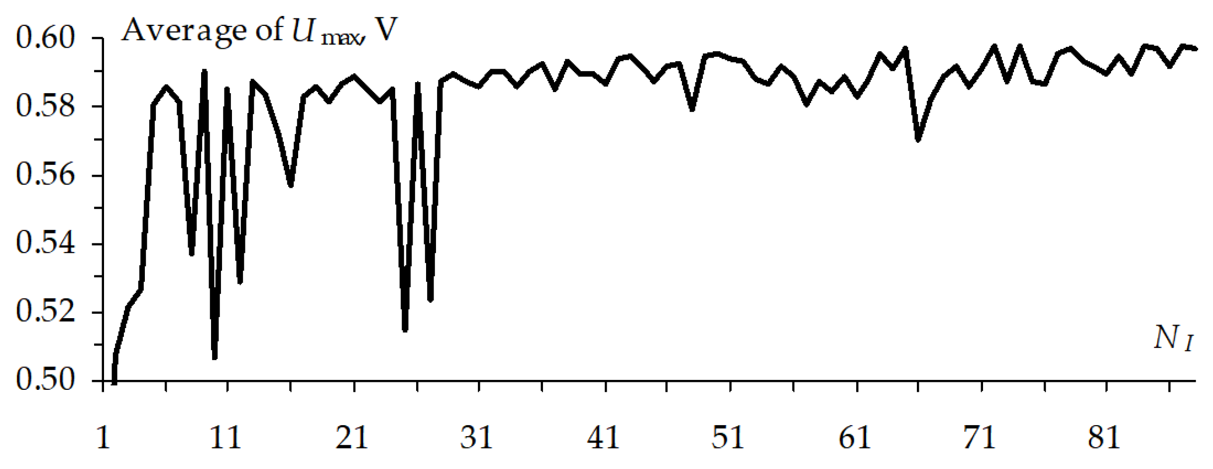
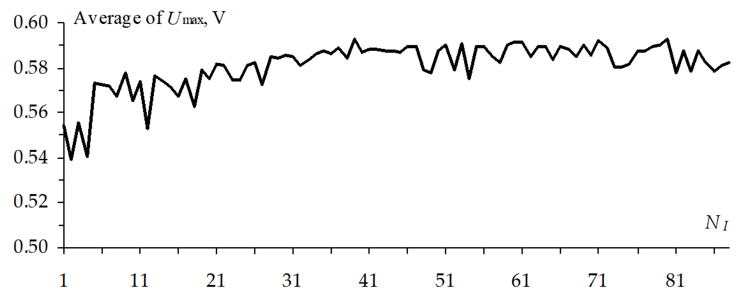
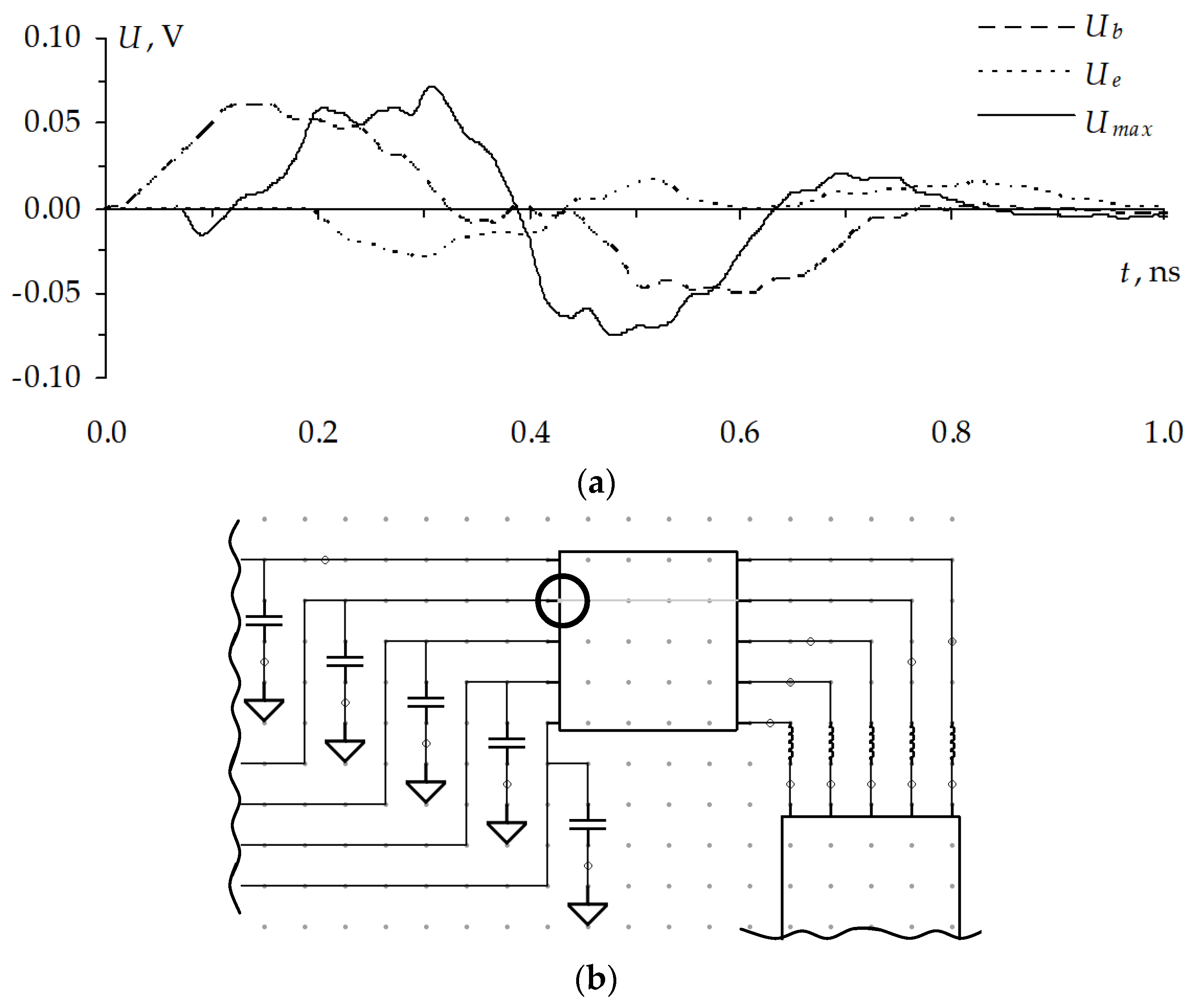
The Umax arithmetic averages (of 10 runs) for IS = 3, 0.3, 0.03 ns in their dependence on the ES iteration number (NI) are shown in Figure 35, Figure 36 and Figure 37, respectively. It is necessary to check the appearing of signal peaks along the whole conductor with the use of excitation parameters which have been obtained as a result of the optimization. The voltage waveforms along the active conductor are shown in Figure 38a, where the waveforms are the following: Ub, at the input; Ue, at the end; and Umax, with the highest peak voltage. The voltage maximum localization is shown in Figure 38b. The voltage waveforms calculated along the passive (nearest to active) conductor with the highest amplitude of the crosstalk and its maximum localization are presented in Figure 39.
Consider the results of the optimization presented in Table 7. They show that all Umax values are very similar and differ in the fourth decimal place. The same situation is observed with the best solutions obtained after each ES cycle – the differences are near 5 ps. The highest Umax is obtained in the first ES run for all ISs. The small differences in the obtained results hardly change the voltage waveforms calculated in the V34 node. As we can see from Figure 34, the signal waveforms coincide.
Consider the Umax arithmetic average for each IS. The strongest change of Umax is observed when IS = 300 ps, starting from 0.5 V (Figure 36). However, after 30th calculation, it becomes almost the highest and other changes are within the bounds of 30 mV. Before the 30th calculation, the Umax change has strong spikes, which are possibly caused by a strong mutation of an offspring. When IS = 3 ns (Figure 35), the Umax arithmetic average has a smooth rising character without strong spikes (in the range up to 30 mV) and starting at 0.52 V it reaches the maximum value in the 69th calculation, and when IS = 30 ps (Figure 37), the Umax changes the least of all and starting at 0.55 mV it reaches the maximum in the 39th calculation.
Consider the voltage waveforms with the localized maximums. The maximum is localized in segment 1 of the same MCTL section both in the active (Figure 38) and passive (Figure 39) conductors. The ultrashort pulse maximum in the active conductor is 598 mV, which is 20% higher than at the steady state level. The maximum in the passive conductor is 70 mV, which is 14% of the steady state level in the active conductor.
This investigation shows the importance of using ES for optimization for detecting and localizing signal extreme points under the excitation of the ultrashort pulse with various durations. The highest peak level of the active conductor (20% higher than at the steady state level) and the crosstalk of 14% of the steady state level are detected for 325 ps ultrashort pulse. It is also shown that if the IS changes towards the best solution, it does not influence the optimization result.
9. Conclusions

Thus, we have developed an approach which is implemented as a special program module in TALGAT software for simulating electromagnetic compatibility problems. Various investigations into detecting and localizing signal extreme points using the approach were made as follows: in a meander line with two turns (the voltage maximum exceeding the signal amplitude at the input by 1.14 times was detected); in a microstrip cross section (the voltage maximum twice as high as the signal amplitude at the input was detected); in a PCB bus of a spacecraft ANS (the voltage maximum exceeding the steady state level by 18% was detected); using GA for optimization (the voltage maximums exceeding the steady state level by 36% and 38% were detected); using ES for optimization (the voltage maximum exceeding the steady state level by 20% was detected); and also under the ESD excitation. Using the proposed approach, the simulation was carried out over 1000 times faster, while maintaining satisfying accuracy. The obtained results show that the use of GAs and ESs allows solving various complex problems. Furthermore, such an approach minimizes the consequences of intentional and unintentional EMI on REE and increases the quality of REE diagnostics. We assume that they will use the approach for analyzing the power supply bus of a spacecraft and other structures in future. Moreover, as it is known that REE diagnostics can be made by amplitude criteria based on the N-norms that C. Baum proposed in 1979 [44], it seems important to combine the proposed approach with these norms in order to improve REE diagnostics.

Author Contributions

Conceptualization, T.R.G.; investigation, R.R.G. and T.T.G.; writing—original draft preparation, R.R.G.; writing—review and editing, T.T.G. and T.G.G.; formal analysis, T.T.G.; supervision, T.G.G.

Funding

This research was funded by the Ministry of Science and Higher Education of the Russian Federation grant number 8.9562.2017/8.9 and the Russian Federation President grant MD-2652.2019.9.

Acknowledgments

Authors thank reviewers for valuable comments that have considerably improved the paper.

Conflicts of Interest

The authors declare no conflict of interest.
Nomenclature

xA coordinate along an MCTL section
V(x)The vector describing the voltage in x
I(x)The vector describing the current in x
SVThe matrix of modal voltages
SIThe matrix of modal voltages
E0, EDThe propagation matrices
γ N k The propagation constant
NkA number of conductors in the k-th MCTL section
lA length of an MCTL section
C1, C2The constant vectors describing the mode amounts
nTLSA parameter describing a number of x
nA number of MCTL sections
VThe vector describing the voltages calculated in each segment of each MCTL section along the whole conductor
WThe matrices describing the lumped memory elements of the network
HThe matrices describing the lumped memoryless elements of the network
DkThe selector matrix that maps the terminal currents of the k-th MCTL section
YkThe conductance matrix of the k-th MCTL section
EThe constant vector with the entries determined by the independent voltage and current sources
LThe matrix of electromagnetic induction
CThe matrix of electrostatic induction
RThe matrix of conductivities
GThe matrices of resistances
trlkA k-th MCTL section
UmaxA maximum voltage value (in the block diagrams)A waveform with the maximum voltage value (in the graphics)
UminA minimum voltage value (in the block diagrams)A waveform with the minimum voltage value (in the graphics)
UbA voltage waveform at the beginning of a conductor
UeA voltage waveform at the end of a conductor

References

  1. Paul, C. Analysis of Multiconductor Transmission Lines; Wiley: New York, NY, USA, 2007; p. 821. [Google Scholar]
  2. Cao, Y.S.; Wang, Y.; Jiang, L.; Ruehli, A.E.; Fan, J.; Drewniak, J.L. Quantifying EMI: A methodology for determining and quantifying radiation for practical design guidelines. IEEE Trans. Trans. Electromagn. Compat. 2017, 59, 1424–1431. [Google Scholar] [CrossRef]
  3. Paoletti, U. On the noise path determination with the noise source modulation technique. IEEE Trans. Electromagn. Compat. 2017, 59, 1400–1407. [Google Scholar] [CrossRef]
  4. Li, P.; Huang, D.; Ruan, J.; Niu, X. EM Measurements between MV switching sources and colocated sensitive circuit. IEEE Trans. Electromagn. Compat. 2015, 57, 513–521. [Google Scholar] [CrossRef]
  5. Mora, N.; Vega, F.; Lugrin, G.; Rachidi, F.; Rubinstein, M. Study and classification of potential IEMI sources. Syst. Des. Assess. Notes 2014, 41, 52. [Google Scholar]
  6. Gizatullin, Z.M.; Gizatullin, R.M. Investigation of the Immunity of Computer Equipment to the Power-Line Electromagnetic Interference. J. Commun. Technol. Electron. 2016, 5, 546–550. [Google Scholar] [CrossRef]
  7. Gaynutdinov, R.R.; Chermoshentsev, S.F. Study immunity to disturbance of electronic system aircraft by influences of intentional ultrashort electromagnetic pulses. In Proceedings of the 2016 International Conference on Actual Problems of Electron Devices Engineering (APEDE), Saratov, Russia, 22–23 September 2016; pp. 1–6. [Google Scholar] [CrossRef]
  8. Moser, K.; Andersen, A.; Dennison, J.R. Dependence of electrostatic field strength on voltage ramp rate for spacecraft materials. IEEE Trans. Plasma Sci. 2017, 45, 2036–2039. [Google Scholar] [CrossRef]
  9. Huang, L.; Gao, C.; Guo, F.; Sun, C. Lightning Indirect Effects on Helicopter: Numerical Simulation and Experiment Validation. IEEE Trans. Electromagn. Compat. 2017, 59, 1171–1179. [Google Scholar] [CrossRef]
  10. Cabello, M.R.; Fernandez, S.; Pous, M.; Pascual-Gil, E.; Angulo, L.D.; Lopez, P.; Riu, P.J.; Gutierrez, G.G.; Mateos, D.; Poyatos, D.; et al. SIVA UAV: A case study for the EMC analysis of composite air vehicles. IEEE Trans. Electromagn. Compat. 2017, 59, 1103–1113. [Google Scholar] [CrossRef]
  11. Wang, D.; Yang, S.; Wang, L.; Liu, W. Hardware-in-the-loop simulation for aircraft electric power system. In Proceedings of the 2016 International Conference on Electrical Systems for Aircraft, Railway, Ship Propulsion and Road Vehicles & International Transportation Electrification Conference (ESARS-ITEC), Toulouse, France, 2–4 November 2016; pp. 1–5. [Google Scholar] [CrossRef]
  12. Yuqing, L.; Tianshe, Y.; Jian, L.; Na, F.; Guan, W. A fault diagnosis method by multi sensor fusion for spacecraft control system sensors. In Proceedings of the 2016 IEEE International Conference on Mechatronics and Automation, Harbin, China, 7–10 August 2016; pp. 748–753. [Google Scholar] [CrossRef]
  13. Shiue, G.H.; Shiu, J.H.; Chiu, P.W. Analysis and design of crosstalk noise reduction for coupled striplines inserted guard trace with an open-stub on time-domain in high-speed digital circuits. IEEE Trans. Compon. Packag. Manuf. Technol. 2011, 1, 1573–1582. [Google Scholar] [CrossRef]
  14. Farhan, M.A.; Gad, E.; Nakhla, M.S.; Achar, R. New method for fast transient simulation of large linear circuits using high-order stable methods. IEEE Trans. Compon. Packag. Manuf. Technol. 2013, 3, 661–669. [Google Scholar] [CrossRef]
  15. Hao, H.; Xia, Y. Vibration-based damage detection of structures by genetic algorithm. J. Comput. Civ. Eng. 2002, 16, 222–229. [Google Scholar] [CrossRef]
  16. Cheng, X.; Ciuonzo, D.; Rossi, P.S. Multi-bit decentralized detection through fusing smart & dumb sensors based on rao test. IEEE Trans. Aerosp. Electron. Syst. 2019. [Google Scholar] [CrossRef]
  17. Moreno, L.; Armingol, J.M.; Garrido, S.; de la Escalera, A.; Salichs, M.A. A genetic algorithm for mobile robot localization using ultrasonic sensors. J. Intell. Robot. Syst. 2002, 34, 135–154. [Google Scholar] [CrossRef]
  18. Sardellitti, S.; Scutari, G.; Barbarossa, S. Joint optimization of radio and computational resources for multicell mobile-edge computing. IEEE Trans. Signal Inf. Process. Netw. 2015, 1, 89–103. [Google Scholar] [CrossRef]
  19. Pazos, S.; Hurtado, M.; Muravchik, C.H.; Nehorai, A. Projection matrix optimization for sparse signals in structured noise. IEEE Trans. Signal Process. 2015, 63, 3902–3913. [Google Scholar] [CrossRef]
  20. Rubio, J.; Iserte, A.P.; Palomar, D.P.; Goldsmith, A. Joint optimization of power and data transfer in multiuser MIMO systems. IEEE Trans. Signal Process. 2016, 65, 212–227. [Google Scholar] [CrossRef]
  21. Yin, F.; Zhao, Y.; Gunnarsson, F.; Gustafsson, F. Received-signal-strength threshold optimization using gaussian processes. IEEE Trans. Signal Process. 2017, 65, 2164–2177. [Google Scholar] [CrossRef]
  22. Denisova, L.A.; Meshcheryakov, V.A. Control system synthesis based on multicriteria optimization using genetic algorithm. In Proceedings of the 2017 Dynamics of Systems, Mechanisms and Machines (Dynamics), Omsk, Russia, 14–16 November 2016; pp. 1–5. [Google Scholar]
  23. Mohammed, H.J.; Abdulsalam, F.; Abdulla, A.S.; Ali, R.S.; Alhameed, R.A.A.; Noras, J.M.; Abdulraheem, Y.L.; Ali, A.; Rodriguez, J.; Abdalla, A.M. Evaluation of genetic algorithms, particle swarm optimisation, and firefly algorithms in antenna design. In Proceedings of the Synthesis, Modeling, Analysis and Simulation Methods and Applications to Circuit Design (SMACD), Lisbon, Portugal, 27–30 June 2016; pp. 1–4. [Google Scholar]
  24. Goudos, K.; Kalialakis, C.; Mittra, R. Evolutionary algorithms applied to antennas and propagation: A review of state of the art. Int. J. Antennas Propag. 2016, 2016, 1010459. [Google Scholar] [CrossRef]
  25. Cheng, Y.S.; Wu, R.B. Direct eye diagram optimization for arbitrary transmission lines using fir filter. IEEE Trans. Compon. Packag. Manuf. Technol. 2011, 1, 1250–1258. [Google Scholar] [CrossRef]
  26. Kwak, N.S.; Lee, J.; Jang, Y.H. Genetic-algorithm-based controlling of microcontact distributions to minimize electrical contact resistance. IEEE Trans. Compon. Packag. Manuf. Technol. 2012, 2, 1768–1776. [Google Scholar] [CrossRef]
  27. Zhang, M.S.; Tan, H.Z.; Mao, J.F. Signal-integrity optimization for complicated multiple-input multipleoutput networks based on data mining of s-parameters. IEEE Trans. Compon. Packag. Manuf. Technol. 2014, 4, 1184–1192. [Google Scholar] [CrossRef]
  28. Liu, H.J.; Jain, R.; Rajawat, K. Asynchronous decentralized dynamic optimization for power network voltage control. IEEE Trans. Signal Inf. Process. Netw. 2016, 3, 568–579. [Google Scholar] [CrossRef]
  29. Chung, C.; Lee, S.; Kwak, B.M.; Kim, G.; Kim, J. A delay line circuit design for crosstalk minimization using genetic algorithm. IEEE Trans. Comput. Aided Des. Integr. Circuits Syst. 2008, 27, 578–583. [Google Scholar] [CrossRef]
  30. Gazizov, R.R.; Zabolotsky, A.M.; Orlov, P.E. Signal maximum localization in multiconductor transmission lines of printed circuit boards using TALGAT system. Dokl. Tom. Gos. un-ta System upr. i Radioelectroniki 2015, 38, 147–150. (In Russian) [Google Scholar]
  31. Gazizov, R.R.; Zabolotsky, A.M.; Gazizov, T.T. Research on ultrashort pulse propagation in microstrip C-section with variated separation between coupled conductors. Dokl. Tom. Gos. un-ta System upr. i Radioelectroniki 2016, 19, 79–82. (In Russian) [Google Scholar]
  32. Gazizov, R.R.; Zabolotsky, A.M.; Gazizov, T.T.; Belousov, A.O. Influence of ultrashort pulse duration on its peak values localization in PCB of spacecraft autonomous navigation system. In Proceedings of the 18th International Conference of Young Specialists on Micro/Nanotechnologies and Electron Devices, Erlagol, Russia, 29 June–3 July 2017; pp. 69–74. [Google Scholar] [CrossRef]
  33. Gazizov, R.R.; Belousov, A.O.; Gazizov, T.T. Influence of ultrashort pulse duration on localization of crosstalk peak values in PCB of spacecraft autonomous navigation system. In Proceedings of the International Siberian Conference on Control and Communications (SIBCON 2017), Astana, Kazakhstan, 29–30 June 2017; pp. 1–6. [Google Scholar] [CrossRef]
  34. Gazizov, R.R.; Belousov, A.O.; Gazizov, T.T.; Gazizov, T.R. Optimization of ultrashort pulse duration with usage of genetic algorithms by criteria of peak voltage maximization in PCB bus. In Proceedings of the IEEE 2017 Siberian Symposium on Data Science and Engineering (SSDSE), Novosibirsk, Russia, 12–13 April 2017; pp. 1–5. [Google Scholar] [CrossRef]
  35. Gazizov, R.R.; Ryabov, R.S.; Gazizov, T.T. Influence of crossover and mutation coefficients on GA optimization of ultrashort pulse duration by criteria of peak voltage maximization in PCB bus. In Proceedings of the IEEE 2017 International Multi-Conference on Engineering, Computer and Information Sciences (SIBIRCON), Novosibirsk, Russia, 18–24 September 2017; pp. 415–420. [Google Scholar] [CrossRef]
  36. Zabolotsky, A.; Gazizov, T. Time Response of Multiconductor Transmission Lines; Tomsk State University: Tomsk, Russia, 2007; p. 152. [Google Scholar]
  37. Kuksenko, S.P.; Gazizov, T.R.; Zabolotsky, A.M.; Ahunov, R.R.; Surovtsev, R.S.; Salov, V.K.; Lezhnin, E.V. New developments for improved simulation of interconnects based on method of moments. Advances in Intelligent Systems Research. In Proceedings of the 2015 International Conference on Modeling, Simulation and Applied Mathematics, Phuket, Thailand, 23–24 August 2015; pp. 293–301. [Google Scholar] [CrossRef]
  38. Gazizov, R.R. Simulation of ESD effects on PCB bus of spacecraft autonomous navigation system. In Proceedings of the IEEE 2017 International Multi-Conference on Engineering, Computer and Information Sciences (SIBIRCON), Novosibirsk, Russia, 18–24 September 2017; pp. 501–505. [Google Scholar] [CrossRef]
  39. Gazizov, T.R.; Dolganov, E.S.; Zabolotsky, A.M. Modal filter as a device for electrostatic discharge protection of onboard computers and control units of space vehicles. Russ. Phys. J. 2012, 55, 282–287. [Google Scholar] [CrossRef]
  40. IEC 61000-4-2 (2003). Electromagnetic Compatibility (EMC) Part 4: Testing and Measurement Techniques—Section 2: Electrostatic Discharge Immunity Test; IEC: Geneva, Switzerland, 2003. [Google Scholar]
  41. Gazizov, R.R.; Kuharenko, M.N.; Gazizov, T.R. Optimization of PCB bus loads with usage of genetic algorithms by criteria of peak voltage minimization. In Proceedings of the 2017 Dynamics of Systems, Mechanisms and Machines (Dynamics), Omsk, Russia, 14–16 November 2017; pp. 1–5. [Google Scholar] [CrossRef]
  42. Beyer, H. Evolution strategies. Scholarpedia 2007, 2, 1965. [Google Scholar] [CrossRef]
  43. Hansen, N. Python: Module Barecmaes2. Lri.fr. 2017. Available online: https://www.lri.fr/~hansen/bare cmaes2.html (accessed on 17 November 2017).
  44. Baum, C. Norms and Eigenvector Norms. Math. Notes 1979, 63, 1–42. [Google Scholar]
Figure 1. Approach for signal extreme points detection and localization.
Symmetry 11 01209 g001
Figure 2. Block diagram of the visualization algorithm of signal propagation along the circuit.
Symmetry 11 01209 g002
Figure 3. Block diagram of the algorithm for defining the allowed ways of signal propagation along the circuit.
Symmetry 11 01209 g003
Figure 4. Test circuit diagram.
Symmetry 11 01209 g004
Figure 5. Display of each step of the algorithm before the complete processing of the first circuit component.
Symmetry 11 01209 g005
Figure 6. All allowed end nodes B for the test circuit diagram.
Symmetry 11 01209 g006
Figure 7. Signal localization example.
Symmetry 11 01209 g007
Figure 8. Block diagram of the algorithm for detecting and localizing signal extreme points.
Symmetry 11 01209 g008
Figure 9. The circuit diagram (a) and the cross section (b) of the meander line with two turns.
Symmetry 11 01209 g009
Figure 10. Comparison of the signal waveforms with the voltage maximum.
Symmetry 11 01209 g010
Figure 11. The circuit diagram (a) and the cross section (b) of the meander line with one turn.
Symmetry 11 01209 g011
Figure 12. Voltage waveforms with s = 400 mm (a) and 8 μm (b).
Symmetry 11 01209 g012
Figure 13. Comparison of the signal waveforms with the voltage maximum.
Symmetry 11 01209 g013
Figure 14. Investigated bus on printed circuit board (PCB) fragment.
Symmetry 11 01209 g014
Figure 15. Circuit diagram of the PCB bus in TALGAT software.
Symmetry 11 01209 g015
Figure 16. Excitation pulse waveforms with different durations.
Symmetry 11 01209 g016
Figure 17. Signal waveforms obtained under the excitations U1 (a), U2 (b), and U3 (c).
Symmetry 11 01209 g017
Figure 18. Location of maximums (a and b) for signals from Figure 17b,c, respectively, and also the location of minimum (c) for a signal from Figure 17c.
Symmetry 11 01209 g018
Figure 19. Diagram fragment with four generators.
Symmetry 11 01209 g019
Figure 20. Waveforms along conductor 3 under the excitations U1 (a), U2 (b), and U3 (c).
Symmetry 11 01209 g020
Figure 21. Maximum locations for signals from Figure 20b (a) and и Figure 20c (b).
Symmetry 11 01209 g021
Figure 22. Waveforms along conductor 3 with active conductors 1, 2, 4, and 5.
Symmetry 11 01209 g022
Figure 23. Waveforms along conductor 1 with active conductors 1, 2, 4, and 5.
Symmetry 11 01209 g023
Figure 24. Umax values for five GA runs with different n.
Symmetry 11 01209 g024
Figure 25. Voltage waveforms along the active conductor (a) and the voltage maximum location (b).
Symmetry 11 01209 g025
Figure 26. Voltage waveforms along the passive conductor (a) and the crosstalk maximum location (b).
Symmetry 11 01209 g026
Figure 27. Convergence diagrams of the fitness function values for each run with km = 0.03 (a) and the arithmetic average of runs with different km (b).
Symmetry 11 01209 g027
Figure 28. Convergence diagrams of the fitness function values for each run with kc = 0.8(a) and the arithmetic average of runs with different kc (b).
Symmetry 11 01209 g028
Figure 29. Umin values for ten runs with different n.
Symmetry 11 01209 g029
Figure 30. Dependences of the Umin on n.
Symmetry 11 01209 g030
Figure 31. Signal waveforms for the best fitness function result at I, II, and III points.
Symmetry 11 01209 g031
Figure 32. Signal waveforms at I, II, and III points before using the optimization.
Symmetry 11 01209 g032
Figure 33. Bus under investigation on the PCB fragment.
Symmetry 11 01209 g033
Figure 34. Voltage waveforms for the Umax with different ISs.
Symmetry 11 01209 g034
Figure 35. Dependence of the Umax arithmetic average on NI for IS = 3 ns.
Symmetry 11 01209 g035
Figure 36. Dependence of the Umax arithmetic average on NI for IS = 300 ps.
Symmetry 11 01209 g036
Figure 37. Dependence of the Umax arithmetic average on NI for IS = 30 ps.
Symmetry 11 01209 g037
Figure 38. (a) Voltage waveforms along the active conductor; (b) the voltage maximum location.
Symmetry 11 01209 g038
Figure 39. Voltage waveforms along the passive conductor (a) and the localization of its maximum (b).
Symmetry 11 01209 g039
Table 1. Voltage extreme points and their localization parameters.
ExcitationFigureUmaxUmin
Voltage, VSegment, FigureVoltage, VSegment, Figure
U117a0.5301−0.051
U217b0.59710 (18a)−0.1120
U317c0.5525 (18b)−0.183 (18c)
Table 2. Crosstalk extreme points and their localization parameters.
ExcitationFigureUmaxUmin
Voltage, VSegment, FigureVoltage, VSegment, Figure
U120a0.0311−0.0311
U220b0.1391−0.1265 (21a)
U320c0.2921−0.1998 (21b)
Table 3. Results of five genetic algorithm (GA) runs for five chromosomes.
NPNumber of a Runt, str, nstd, nstf, nsUmax, V
51441.4070.9890.01140.8000.551147
2452.4370.5000.01990.8790.545629
3486.6920.4470.03560.5820.534152
4486.5080.7070.02510.1270.531801
5510.5640.1110.05500.9540.524602
101983.8700.6630.01190.9250.550284
21045.060.4870.01000.7720.551331
31133.290.4290.01020.6520.549775
41204.640.8940.01110.9230.550668
51280.820.9510.01840.7190.547373
5013679.800.91600.01080.8740.551185
23689.230.39800.01140.9380.551207
33686.370.73000.01030.7610.551353
43649.920.01350.01040.8200.553568
53673.960.65800.01030.7890.551315
7515951.780.74020.011230.9310.551358
25707.050.01230.012140.5490.554590
35479.930.62610.010450.7850.551505
45818.870.01080.014320.6580.552927
55880.290.80170.010310.8700.551700
Table 4. Values of Usum and V with different km for ten GA runs.
Runkm
0.010.030.050.08
10.508190.551590.551080.54131
20.516070.551220.551960.55146
30.549130.557040.550050.54974
40.550940.550810.551000.55503
50.507990.552840.550430.55127
60.531530.549200.553170.55092
70.526850.550920.550790.54232
80.539830.552710.552720.55108
90.540090.551100.551280.54909
100.543090.551320.551200.55041
Table 5. Usum and V values with different kc for ten GA runs.
Runkc
0.10.30.50.8
10.554440.552140.551660.55072
20.530830.550130.551770.55128
30.551690.548600.550270.55167
40.550410.549960.550920.52187
50.552790.549880.551210.55254
60.551020.551650.551800.55118
70.551500.551820.547660.55448
80.551200.550600.550400.55024
90.551910.550520.551220.55142
100.550580.551160.551730.55012
Table 6. Umin and mV for different Nr and n.
NRkc
183033555660110260
142861535077454441
28287283521544776535
3584170784794468423
41202345952721875922
5356180464486826235
61052364759143524426
713077443160884728
8115132525471515918
9413491878854766016
101221441543738725435
Table 7. Umax Values for 10 runs of evolution strategies (ES) with different initial solutions (ISs).
ES RunIS, ns
30.30.03
14286153
28287283
358417078
412023459
535618046
610523647
71307744
811513252
941349187
10122144154
The best solution325.53ps330.06ps325.59ps