1. Introduction
During the last five decades, a number of regular papers, review articles and chapters in books, concerning the synthesis and properties of metal 1,2-dithiolene (M 1,2-DT) complexes and selenium analogues, with M = Ni, Pd, Pt, Au, Cu,
etc., have been published (see for example [
1,
2,
3,
4,
5,
6,
7,
8,
9,
10,
11,
12,
13,
14,
15,
16,
17,
18,
19,
20,
21,
22,
23,
24,
25,
26,
27,
28,
29,
30,
31,
32,
33,
34,
35,
36,
37,
38,
39,
40,
41,
42,
43,
44,
45,
46,
47,
48,
49,
50,
51,
52,
53,
54,
55,
56,
57,
58,
59,
60,
61,
62,
63,
64,
65,
66,
67,
68,
69,
70,
71,
72,
73,
74,
75,
76,
77,
78,
79,
80,
81,
82,
83,
84,
85,
86,
87,
88,
89,
90,
91,
92,
93,
94,
95,
96,
97,
98,
99,
100,
101,
102,
103,
104,
105,
106,
107,
108,
109,
110,
111,
112,
113,
114]). The (neutral) complexes are characterized as homoleptic with the general formula (
Figure 1) or heteroleptic such as M(diimine)(dithiolate). The homoleptic are divided in symmetrical with R
1 = R
2 = R
3 = R
4 (R-family, not cyclic), with R
1, R
2 = R
3, R
4 (RR-family, cyclic), with R
1 = R
2 = R
3 = R
4 = SR (SR-family, not cyclic), with R
1, R
2 = R
3, R
4 = S–R–S (SRS-family, cyclic), with R
1, R
2 = R
3, R
4 = N(R)–C(=S)–N(R') (NNR-family, cyclic),
etc., as well as unsymmetrical with R
1 = R
2 ≠ R
3 = R
4(R-family, not cyclic), with R
1, R
2 = RR ≠ R
3, R
4 = R'R' (R'R'-family, cyclic), with R
1, R
2 = S–R–S ≠ R
3, R
4 = S–R'–S (SR'S-family, cyclic),
etc. Some of the simple ligands and their abbreviations are tabulated in
Table 1. Some ligands with complicated edge groups are referred by numbers and tabulated in
Table 2 (see also [
10,
97]). The additional groups to the metal dithiolene core could have donor ability (e.g., OMe, NMe
2) or acceptor ability (e.g., CN, CF
3). The donor (push) or acceptor (pull) ability of the additional groups, plays an important role in the behavior concerning optical, conducting and superconducting properties of these materials. For example, the complexes [M(mnt)
2] [
5] and [M(dmit)
2] [
6] (see also [
8,
11,
12,
20]), of which the molecular formulas are shown in
Figure 2, are based on the ligands with acceptor groups and give cation deficient salts. Since the observation of semiconducting behavior in (Li)
x[Pt(mnt)
2] [
5] and (Bu
4N)
x[Ni(dmit)
2] (1 >
x > 0) ([
6] and references therein), a number of similar complexes based on Ni, Pt, Pd, Cu and Au have been prepared and studied.
Figure 1.
General molecular formula of neutral M 1,2-DT complexes.
Figure 1.
General molecular formula of neutral M 1,2-DT complexes.
Figure 2.
Molecular formulas of Ni(mnt)2 and Ni(dmit)2.
Figure 2.
Molecular formulas of Ni(mnt)2 and Ni(dmit)2.
Table 1.
Simple 1,2-dithiolene ligands and their abbreviations.
Table 2.
Some 1,2-dithiolene ligands referred by numbers.
On the other hand, the complexes [Ni(dddt)
2] [
5] and [Ni(edo)
2] [
14], of which the molecular formulas are shown in
Figure 3, are based on ligands with donor ability and give cationic salts, which are conducting materials [
13,
14,
15,
21].
Figure 3.
Molecular formulas of Ni(dddt)2 and Ni(edo)2.
Figure 3.
Molecular formulas of Ni(dddt)2 and Ni(edo)2.
The M 1,2-DT complexes exhibit some similarities to the so called TTF compounds of the general formula (
Figure 4) and selenium analogues, in which the central metal atom (M) of M 1,2-DTs is replaced by the C=C group (see for example [
12,
16,
21,
85]). Generally, the TTFs such as ET (
Figure 5), exhibit weak semiconducting behaviour with energy gap of 2–3 eV, while M 1,2-DTs are better semiconductors with HOMO/LUMO energy gap smaller than 1.5 eV. Some cationic salts of TTFs exhibit similar behavior to that of M 1,2-DT cationic salts. For example [Ni(dddt)
2]
2X are isostructural and exhibit metallic behavior as (ET)
2X.
Figure 4.
General molecular formula of TTF compounds.
Figure 4.
General molecular formula of TTF compounds.
Figure 5.
Molecular formula of ET.
Figure 5.
Molecular formula of ET.
In recent years, a number of symmetrical M 1,2-DT complexes based on extended TTF-dithiolato ligands, such as [Ni(dt)
2] [
22,
23] and some unsymmetrical such as [Ni(dt)(dmit)] [
48,
49] (
Figure 6) and selenium analogues have been prepared and studied. A number of extended TTF-dithiolate ligands are tabulated in
Table 3. Dithiolene ligands could be coordinated as 1,2-enedithiolate dianions (as in
Table 1,
Table 2 and
Table 3), neutral dithioketones or mixed valence thioketones—radical thiolate monoanions—and have been regarded both as innocent and non-innocent ligands [
6,
7,
8,
9,
10,
49,
68]. These single component (neutral) complexes exhibit semiconducting or metallic behaviour. Review articles, concerning neutral complexes with N coordinated groups [
97] or with ligands of
Table 2 [
102] and articles concerning unsymmetrical complexes (of the type push-pull) [
95], have been reported recently.
Figure 6.
Molecular formulas of Ni(dt)2 and Ni(dt)(dmit).
Figure 6.
Molecular formulas of Ni(dt)2 and Ni(dt)(dmit).
Table 3.
Extended TTF 1,2-dithiolene ligands and their abbreviations.
This paper is an overview of the published work concerning the preparation, properties and possible applications of semiconducting neutral (single component) complexes based on Ni, Pt, Pd, Cu, Au and on some ligands of
Table 1,
Table 2 and
Table 3. Mainly, the work published since 2005 is considered [
1,
2,
3,
4,
5,
6,
7,
8,
9,
10,
11,
12,
13,
14,
15,
16,
17,
18,
19,
20,
21,
22,
23,
24,
25,
26,
27,
28,
29,
30,
31,
32,
33,
34,
35,
36,
37,
38,
39,
40,
41,
42,
43,
44,
45,
46,
47,
48,
49,
50,
51,
52,
53,
54,
55,
56,
57,
58,
59,
60,
61,
62,
63,
64,
65,
66,
67,
68,
69,
70,
71,
72,
73,
74,
75,
76,
77,
78,
79,
80,
81,
82,
83,
84,
85,
86,
87,
88,
89,
90,
91,
92,
93,
94,
95,
96,
97,
98,
99,
100,
101,
102,
103,
104,
105,
106,
107,
108,
109,
110,
111,
112,
113,
114]. The results, obtained from unsymmetrical complexes in comparison to the corresponding symmetrical ones in the solid state, are mainly discussed. They are compared to those obtained from the corresponding TTFs and similar single component materials. More information concerning the ligands of
Table 1 can be found in [
6,
7,
8,
9,
10,
11,
12,
13,
14,
15,
16,
20,
21,
24,
26,
27,
28,
30,
31,
34,
36,
48,
49,
50,
53,
61,
62,
63,
64,
72,
77,
79,
88,
89,
92,
94,
100,
101,
102,
103,
104]. More information concerning the ligands of
Table 2 can be found in the corresponding references for L1 [
34], L2 [
34,
98], L3 [
33,
95,
102], L4 [
56,
73,
102], L5 [
97], L6 [
61], L7 [
75], L8 [
58,
60], L9 [
56,
60,
79,
84,
101,
110,
111], L10 [
38,
62,
65,
79,
101,
102,
110], L11 [
109,
113], L12 [
93,
102], L13 [
114], L15 [
33,
102,
114], L16 [
57,
102], L17 [
102], and L18 [
93,
102]. More information concerning the ligands of
Table 3 can be found in the references [
22,
23,
30,
45,
46,
48,
49,
90]. Some related papers are given in references [
115,
116,
117,
118,
119,
120,
121,
122,
123,
124,
125,
126,
127,
128,
129,
130,
131,
132,
133,
134,
135,
136,
137,
138,
139]. They concern properties of TTFs [
117,
130,
131,
132,
133], structural [
115,
123], and electronic [
118,
119,
120,
121] properties of solids, electrochemical aspects [
122], saturable absorbers [
121] and field effect transistors [
116,
124,
125,
126,
127,
128,
129,
134,
135,
136,
137,
138].
3. Structural Properties
In the most neutral M 1,2-DTs, the ligand forms a strictly square-planar arrangement, with all S–M–S bond angles very close to 90°, but with variation in the value of intermolecular S–S contacts. The neutral complexes may exist as planar monomers or form dimers with either metal-metal bonds or metal-sulfur (selenium) bonds. Most of M 1,2-DTs were found to be crystallized in centrosymmetric space group and, up to now, only three complexes have been found to be crystallized in non centrosymmetric space group (see [
7,
10,
15,
17,
20,
63,
64,
69,
94,
97]). The data from selected M 1,2-DTs are described here, starting from crystals with weak intermolecular interactions.
The symmetrical complex α-[Ni(dpedt)
2], for example is crystallized in the centrosymmetric space group P2
1/n, where Ni–S = 2.10, C–S = 1.71, C–C = 1.37 Å, S–Ni–S = 89.8, Ni–S–C = 107.3, S–C–C = 118° [
3,
79]. The symmetrical complex [Au(dpedt)
2] is crystallized in the tricliric space group P1 and is isostructural with β-[Ni(dpedt)
2], but not isostructural with α-[Ni(dpedt)
2], [Pt(dpedt)
2] and [Pd(dpedt)
2] [
2,
3,
7,
9].
Figure 9 shows the packing diagram of [Au(dpedt)
2] [
79]. In the molecules the Au–S, C–S and the olefinic C–C bond lengths are
ca. 2.29, 1.73, 1.37 Å, respectively. The bond lengths M–S for the corresponding complexes of several metals (M) increase in the order Au–S > Pd–S > Pt–S > Ni–S. In the cell of [Au(dpedt)
2] the molecules are stacked along the
b-axis. Both interstacking and intrastacking S–S intermolecular distances are
ca. 4.5 Å,
i.e., much larger than the sum of van der Waal’s radii (3.7 Å), while in (Bu
4N)[M(dmit)
2] these distances are 3.59–3.72 Å (see [
20] and references therein). This means that the complex has an almost 3D structure, with weak S–S interactions. The long axis of the needle shaped crystals is almost parallel to the
a-axis. In the samples they have not been found in other habits. Some complexes of the type [Ni(L9)
2] [
56], [Ni(L6)
2] [
61], and similar compounds of Au with ligands containing long chain groups [
89,
110] are isostructural with [Au(dpedt)
2] [
79]. In [Au(bdt)
2], isostructural with α-[Ni(dpedt)
2], the S–S contacts are 3.60–3.66 Å [
29].
Figure 9.
Packing diagram of a crystal of [Au(dpedt)
2]. Reproduced from [
79] with permission from Elsevier, and photograph of a crystal.
Figure 9.
Packing diagram of a crystal of [Au(dpedt)
2]. Reproduced from [
79] with permission from Elsevier, and photograph of a crystal.
In the structure of symmetrical [Ni(dddt)
2] [
13,
14], as in [Ni(dmit)
2] [
69], two molecules (A, B) of the complex form independent uniform stacks along the
b-axis. As in the crystal of neutral ET (
i.e., BEDT-TTF), there exists a dimer structure. Within the stacks of [Ni(dddt)
2] the Ni–Ni is 4.67 Å. There is no short intermolecular S–S contact (<3.70 Å) within the stack, and between molecules of adjacent stacks (see [
13,
14] and references therein). In the structure of the symmetrical [Ni(edo)
2] (
Figure 10) the molecules are planar, as in the case of [Ni(dddt)
2], while in the corresponding TTFs (
i.e., BO and ET) are non-planar. The unit cell of [Ni(edo)
2] contains two molecules, each of which is repeated uniformly along the c-axis. The Ni–S bond lengths in [Ni(edo)
2] are slightly larger than that in [Ni(dddt)
2] (2.12 Å).
Figure 10.
Crystal structure of [Ni(edo)
2]. Reproduced from [
14] with permission of the Royal Society of Chemistry.
Figure 10.
Crystal structure of [Ni(edo)
2]. Reproduced from [
14] with permission of the Royal Society of Chemistry.
The neutral [Ni(dmit)
2], studied years ago (see [
20,
69] and references therein), which is crystallized in plate-like crystals of monoclinic space group P2
1/a, show that the molecules stack along the [010] direction, making an angle with the normal to the molecule main plane of 48°. Within the stack, the Ni–Ni spacing is 5.302 Å and the plane to plane distance 3.562 Å. In contrast to that observed in the structure of (Bu
4N)[Ni(dmit)
2], (see [
20,
69] and references therein), in the structure of [Ni(dmit)
2] there are short S–S contacts between adjacent stacks involving the thioacetone sulfur atom (
ca. 3.58 Å) [
69]. The complex [Ni(etoddt)
2] (
Figure 11) [
100] crystallizes in the triclinic space group Pl, and as in the case of [Au(dpedt)
2] [
79] there are no S–S contacts smaller than the sum of the van der Waals radii.
Figure 11.
Schematic presentation of the structure of [Ni(etoddt)2].
Figure 11.
Schematic presentation of the structure of [Ni(etoddt)2].
The unsymmetrical complexes [Ni(pddt)(dmio)], [Ni(tmedt)(dddt)], and [Ni(tmedt)(dmit)] are isostructural and crystallized in the monoclinic space group P2
1/c [
36,
64].
Figure 12 shows a perspective view of the [Ni(pddt)(dmio)] structure and a photography of the crystal. In a layer almost parallel to the
ab-plane there are S–S intermolecular contacts of 3.49 and 3.66 Å. In the other directions the distances are larger. In [Ni(tmedt)(dddt)] and [Ni(tmedt)(dmit)] these contacts are 3.59 and 3.70–3.73 Å, respectively. The intermolecular contacts form a quasi-two-dimensional (q-2D) network. It was found that the largest surface of the crystal is parallel to the crystallographic
ab-plane.
Figure 12.
Perspective view of the [Ni(pddt)(dmio)], reproduced from [
36] with permission of the Verlag der Zeitschrift für Naturforschung, and photograph of crystal [
77].
Figure 12.
Perspective view of the [Ni(pddt)(dmio)], reproduced from [
36] with permission of the Verlag der Zeitschrift für Naturforschung, and photograph of crystal [
77].
The complex [Ni(dmeds)(dmit)] crystallizes in the triclinic space group P1.
Figure 13 shows that the partial labeled plot of complex showing the intermolecular contacts [
50]. The structure consists of centrosymmetric dimers [
7] with the inversion center sitting on the center of the Ni
2Se
2 core. The closest Ni–S and Ni–Se bond lengths in the coordination sphere are
ca. 2.2 and 2.3 Å respectively, while the longer Ni–Se bond (2.56 Å) is responsible for the formation of the dimers. The closest intramolecular Ni–Ni distance is
ca. 3.06 Å. It was found that the largest surface of the rectangular crystals is almost parallel to the crystallographic
ab-plane. There are S–S and S–Se intermolecular contacts of 3.594 and 3.560 Å, respectively, slightly smaller than the sums of van der Waals radii (3.70 and 3.82 Å, respectively), which give rise to the formation of layers almost parallel to the
ab-plane. In other directions the distances are larger. This indicates a
quasi two dimensional behavior of the material.
Figure 13.
Partial labeled plot of [Ni(dmeds)(dmit)], reproduced from [
50] with permission of the Verlag der Zeitschrift für Naturforschung, and photograph of crystal [
77].
Figure 13.
Partial labeled plot of [Ni(dmeds)(dmit)], reproduced from [
50] with permission of the Verlag der Zeitschrift für Naturforschung, and photograph of crystal [
77].
The unsymmetrical complexes [Pd(dpedt)(dddt)], [Ni(dpedt)(dddt)] and [Ni(dpedt)(pddt)] are isostructural and are crystallized in the orthorhobic non-centrosymmetric space group Pbc2
1 [
63,
64,
94].
Figure 14 shows the stacking of [Pd(dpedt)(dddt)] molecules in a column along the
c-axis. However, there is no pseudocentro-symmetrical arrangement of molecules [
20]. It was found that the needle axis of the crystal is the
c-axis. The shortest S–S distance in [Pd(dpedt)(dddt)] is 3.714 Å. The intermolecular contacts form a q-1D network. In [Ni(dpedt)(dddt)] [
64] and [Ni(dpedt)(pddt)] [
94] these distances are 3.764 and 3.738 Å, respectively, which are a little larger than the sums of van der Waals radii (3.70 Å).
In some cases of unsymmetrical M 1,2-DTs, where one of the ligands has a push character (dithione) and the other a pull character (dithiolate), the C–S and C–C distances in the two ligands are different [
31,
80,
95]. For example, in [Ni(Pr
2timdt)(dmit)], the C–S and C–C distances for the ligand Pr
2timdt are 1.69 and 1.38 Å, while for the ligand dmit the distances are 1.74 and 1.29 Å, respectively. In [Ni(tmedt)(dddt)] the push/pull character is weak and the corresponding values for tmedt are 1.68 and 1.37 Å, while for dddt are 1.71 and 1.38 Å [
64,
95]. Similar results as in [Ni(tmedt)(dddt)] have been obtained from non centrosymmetric complexes [Pd(dpedt)(dddt)] [
63], [Ni(dpedt)(dddt)] [
64] and [Ni(dpedt)(pddt)] [
94].
Figure 14.
Crystal structure of [Pd(dpedt)(dddt)]. Reproduced from [
63] with permission of the Verlag der Zeitschrift für Naturforschung, and photograph of crystal [
77].
Figure 14.
Crystal structure of [Pd(dpedt)(dddt)]. Reproduced from [
63] with permission of the Verlag der Zeitschrift für Naturforschung, and photograph of crystal [
77].
In [Ni(dt)(dmit)] and similar complexes with one extended TTF dithiolate ligand there are no crystallographic data. The IR vibrational spectra of [Ni(dt)(dmit)] indicate a dithioglyoxal structure (large HC–CH bond) in the dt ligand of this complex, rather than an olefinic structure (short HC–CH bonds) as in the edt ligand of [Ni(edt)
2] [
49], and consequently, a push/pull behaviour in [Ni(dt)(dmit)] and similar compounds [
48,
89]. It is suggested that the molecular structure has a resonance form similar to that of the push/pull complexes [
95].
In the structure of [Ni(edo)(dmit)], the almost planar molecules are repeated in band to tail fashion along the
c-axis. The average bond lengths of Ni–S, C–S, and C–C are 2.15, 1.70 and 1.39 Å, respectively. In the structure of [Ni(edo)(mnt)], the molecules are arranged alternately along the
c-axis. The average bond lengths of Ni–S, C–S, and C–C are 2.15, 1.62 and 1.32 Å, respectively. In the crystal structure of Cu(dmdt)
2, the molecules are not planar [
25]. The ligands have an arrangement similar to that of κ-phase TTFs based organic conductors and superconductors [
12].
The complex [Ni(tmdt)
2], which is based on the extended TTF dithiolate ligand, tmdt, crystallizes into a very simple and compact structure, the triclinic space group Pĩ. The molecules are planar and form a close packed structure. The S–S contacts are 3.44–3.75 Å. The structural features suggest that the complex is a three-dimensional (3D) anisotropic solid [
46]. The complexes [Au(tmdt)
2] and [Pt(tmdt)
2] [
90] are isostructural with [Ni(tmdt)
2] [
45,
46].
Briefly, the examples of structures given herein and those described elsewhere (see [
9,
10,
11,
12,
13,
14,
15,
16,
17,
18,
19,
20,
21,
22,
23,
24,
25,
26,
27,
28,
29,
30,
31,
32,
33,
34,
35,
36,
37,
38,
39,
40,
41,
42,
43,
44,
45,
46,
47,
48,
49,
50,
51,
52,
53,
54,
55,
56,
57,
58,
59,
60,
61,
62,
63,
64,
65,
66,
67,
68,
69,
70,
71,
72,
73,
74,
75,
76,
77,
78,
79,
80,
81,
82,
83,
84,
85,
86,
87,
88,
89,
90,
91,
92,
93,
94,
95,
96,
97,
98,
99,
100,
101,
102,
103,
104,
105,
106,
107,
108,
109,
110,
111,
112,
113,
114] and references therein) show the existence of a variety of three and low dimensional networks formed from short or large M–S, S–S,
etc. contacts. The nature of the individual molecules plays an important role in the unique intermolecular interactions. From the crystallographic data and the transfer integrals the electronic band structure could be calculated [
18,
20,
51]. Consequently, it is expected that there is also a wide variety in behavior, concerning electronic (see [
7,
18]) and other (see [
2,
3,
4,
6,
7,
8,
9,
10,
11,
12,
13,
14,
15,
17,
19,
20,
21,
22,
23,
24,
25,
26,
27,
28,
29,
30,
31,
32,
33,
34,
35,
36,
37,
38,
39,
40,
41,
42,
43,
44,
45,
46,
47,
48,
49,
50,
51,
52,
53,
54,
55,
56,
57,
58,
59,
60,
61,
62,
63,
64,
65,
66,
67,
68,
69,
70,
71,
72,
73,
74,
75,
76,
77,
78,
79,
80,
81,
82,
83,
84,
85,
86,
87,
88,
89,
90,
91,
92,
93,
94,
95,
96,
97,
98,
99,
100,
101,
102,
103,
104,
105,
106,
107,
108,
109,
110,
111,
112,
113,
114,
15,
17,
19]) properties of M 1,2-DTs, in the solid state.
4. Optical Properties
The optical properties of M 1,2-DTs in the form of single crystals, polycrystalline pellets, thin film (or deposits), suspensions, composites and solutions have been reported in a number of papers. It was observed, years ago, that the optical absorption (OA) spectra of solutions of monoanionic M 1,2-DTs (M = Ni, Pd, Pt), which are paramagnetic compounds, exhibit strong bands, which span the range 700 to
ca 1900 nm, depending on the nature of the metal, the ligand and the solvent (see for examples [
10,
18,
34,
63,
70]). The bands have been interpretated as the HOMO-LUMO transitions or as ligand-to-ligand (LL) charge transfer (CT) transitions [
34,
95]. These bands and the bands of the isoelectronic neutral Au 1,2-DTs have an unsymmetrical shape. After a Gaussian decovolution it has been found that the bands are dominated by two transitions: one intense at low frequency is assigned to 1b
1u→2b
2g (
x-polarized) and one medium to 1a
1u→2b
2g (
y-polarized), as well as some weaker ones [
18,
34]. The experimental values of transitions,
i.e., the band position and intensity of OA bands, have been found to be in reasonable agreement with the theoretically calculated ones [
18,
34]. The splitting of the low frequency band is more discreet in the OA (and reflectance) spectra of the complexes in the solid state (see for example [
29] and refs. [
9,
10,
11] cited therein).
Figure 15 shows the polarized reflectance spectra of (Bu
4N)[Ni(dmit)
2] with the wavevector of the light parallel (R
║) and perpendicular (R
┴) to the needle axis of the crystal, as well as the OA spectra of the material in CS
2 solution and a suspension in CCl
4. The reflectance spectra show anisotropic behavior due to the low dimensional structure of the material [
20,
120]. In parallel polarization the band is split into two sub-bands at 1100 and 1350 nm. The reflectance spectrum of a polycrystalline pellet shows the same bands, while the spectra of a suspension of the material in CCl
4 and that of the solution in CS
2 show narrow bands at
ca. 1204 nm, with an unsymmetrical shape.
Figure 15.
Polarized reflectance spectra of (Bu
4N)[Ni(dmit)
2], optical absorption (OA) spectrum of a suspension of material in CCl
4 (solid line) and of solution in CS
2 (dashed line) [
77].
Figure 15.
Polarized reflectance spectra of (Bu
4N)[Ni(dmit)
2], optical absorption (OA) spectrum of a suspension of material in CCl
4 (solid line) and of solution in CS
2 (dashed line) [
77].
Different results have been obtained from cation deficient complexes. The reflectance spectra of polycrystalline pellets of (Bu
4N)
x[Ni(dmit)
2] and (Bu
4N)
x[Pt(dmit)
2], obtained after oxidation of monoanionic salts with iodine or bromine [
6,
12,
47], are shown in
Figure 16. In these cation-deficient complexes (which behave as mixed-valence complexes) with
x = 0.25 and
x = 0.2, respectively, the low frequency band-position, -intensity, and -shape depend on the
x-value. When
x→0, the (neutral) complex exhibits a narrow band, blue shifted from that of monoanionic (
x = 1), while for intermediate values of x, the complex exhibits a new band at lower frequencies. The reflectance spectra of
Figure 16 seem to be the superposition of those of a mixture of cation-deficient and neutral complexes. Strong OA bands of cation deficient complexes (Bu
4N)
0.06[Au(eddt)
2], (Bu
4N)
0.4[Pt(eddt)
2] and (Bu
4N)
x[Au(dmit)
2] occur at
ca. 860 nm [
40], close to that of (Bu
4N)
0.2[Pt(dmit)
2].
Figure 16.
Reflectance spectra of polycrystalline pellets of (Bu
4N)
x[Ni(dmit)
2] (
a); (Bu
4N)
x[Pt(dmit)
2] (
b). Reproduced from [
54] with permission from Elsevier.
Figure 16.
Reflectance spectra of polycrystalline pellets of (Bu
4N)
x[Ni(dmit)
2] (
a); (Bu
4N)
x[Pt(dmit)
2] (
b). Reproduced from [
54] with permission from Elsevier.
The OA spectra of neutral complexes exhibit strong bands, the position of which depends strongly on the nature of the metal, the ligand the solvent, etc. The OA band positions (and intensities) of unsymmetrical complexes (AB) in solutions occur in between those of the corresponding symmetrical complexes (AA, BB). The characteristic OA wavelength (maximum or onset) is given by the equation:
![Crystals 02 00762 i112]()
(1)
Figure 17 shows the experimentally observed spectra of [Ni(edt)
2], [Ni(edt)(dddt)] and [Ni(dddt)
2] solutions in MeOH [
27]. The observed OA band of the unsymmetrical [Ni(edt)(dddt)] occurs at 864 nm while, the calculated from those of symmetrical and Equation 1 was found at 867 nm.
The OA band position of neutral [Ni(dmit)
2] in solution has been calculated from the positions of the corresponding bands of some symmetrical Ni(L)
2 and unsymmetrical [Ni(L)(dmit)] complexes using Equation 1. It has been found to be
ca. 1070 nm in CS
2 and 1043 nm in CH
3CN. The calculated value for [Ni(dmio)
2] is 932 nm in CS
2. The OA spectra of some Au-based complexes and the OA band position of Pd-based complexes in CS
2 are shown in
Figure 18. It can be seen that the Au-materials exhibit wide transparent spectral regions,
i.e., from
ca. 500 nm to
ca. 1500 nm. It was found that the spectra of [Au(tmedt)(dddt)] and [Au(tmedt)
2] in CS
2 exhibit OA bands at
ca. 1732 and 1500 nm, respectively. Generally, the OA bands of neutral Au 1,2-DTs occur at lower frequencies, even, than those of monoanionic salts of Ni, Pd and Pt, which are isoelectronic (see
Figure 17 and
Figure 18 for examples) [
63,
70]. The OA and reflectance bands of single crystals of [Au(bdt)
2] occur close to 2000 nm [
29].
Figure 17.
UV-vis/near IR absorption spectra of [Ni(dddt)
2] (
a); [Ni(edt)
2] (
b) and [Ni(dddt)(edt)] (
c) in MeOH. Reproduced from [
27] by permission of the Verlag der Zeitschrift für Naturforschung.
Figure 17.
UV-vis/near IR absorption spectra of [Ni(dddt)
2] (
a); [Ni(edt)
2] (
b) and [Ni(dddt)(edt)] (
c) in MeOH. Reproduced from [
27] by permission of the Verlag der Zeitschrift für Naturforschung.
Figure 18.
OA spectra of [Au(dpedt)
2] (
a), [Au(dpedt)(dddt)] (
b) and [Au(dddt)
2] (
c): arrows indicate the OA band positions of [Pd(dpedt)
2] (
d) [Pd(dpedt)(dddt)] (
e) and [Pd(dddt)
2] (
f) in CS
2 [
63,
70].
Figure 18.
OA spectra of [Au(dpedt)
2] (
a), [Au(dpedt)(dddt)] (
b) and [Au(dddt)
2] (
c): arrows indicate the OA band positions of [Pd(dpedt)
2] (
d) [Pd(dpedt)(dddt)] (
e) and [Pd(dddt)
2] (
f) in CS
2 [
63,
70].
The OA spectra of unsymmetrical M 1,2-DTs with a push-pull behavior, such as M(Bz
2pipdt)(mnt) [
95,
106], exhibit broad bands at
ca. 751 (660sh), 651 (560sh) and 685 nm in DMF for M = Ni, Pd, and Pt, respectively, with low to medium molar absorption coefficient and negative solvatochromism [
106]. The OA spectra occur between the spectra of the corresponding symmetrical (if they exist), but do not obey Equation 1. Similar results have been obtained from [Pd(Me
2Pipdt)(dmit)] [
88] solutions in DMSO. In solution four peaks are present, and that at 737 nm may be tentatively assigned to the HOMO-LUMO transition. This band shows negative solvochromism and occurs at higher energy, when compared to the one in the corresponding Ni compound (910 and 965 nm respectively, in CHCl
3).
The position, intensity and shape of the bands in the solid state (single crystals, polycrystalline pellets, thin deposits,
etc.) depend on the structural feature of the complex. If the S–S contacts, for example, are weak as in [Au(dpedt)
2], the position of the OA band of a thin film occurs close to that of the solutions, while, if the S–S contacts are strong as in the [Au(dddt)
2] and [Au(bdt)
2] [
29], the OA bands occur at lower frequencies.
As in the OA spectra of charge transfer (CT) and mixed valence (MV) compounds (see [
117,
120]), the OA onsets or the
Eg values of single component species (i), including small particles of M 1,2-DTs could be obtained from the following Equation 2,
![Crystals 02 00762 i113]()
(2)
where Δ
E is the HOMO/LUMO gap, (
t2)
i and (
t1)
i the corresponding intermolecular transfer integrals. These integrals could be obtained from band structure calculations based on crystallographic data.
Figure 19 shows the schematic presentation of bands and gap (
Eg)
i formation from a one dimensional array of neutral molecules with HOMO/LUMO (H, L) gap of Δ
E, where (
t1)
i and (
t2)
i are the corresponding transfer integrals, for any species (i) concerning bulk (large t) and small particles (small t). If the structure results from dimers, the energy gap is lower than the corresponding levels of dimers [
7,
21,
51].
Figure 20 shows the OA spectra of thin deposits of [Au(dpedt)
2], [Au(dpedt)(dddt)] and [Au(tmedt)
2] obtained by rubbing the complexes on quartz plates. Because of the weak intermolecular interactions in the solid state [
63,
79], the bands occur almost at the same positions as those of the solutions, but are broader, and the fine structure is not clear. The same OA spectra have been obtained from suspensions of the complex in CCl
4 or toluene and from composites of the complex in a polymethylmethacrylate matrix. However, the spectra of films, obtained by a spin-coating technique, showed a fine structure [
79], which could be attributed to several molecular transitions [
34]. However, in the cases of [Ni(etdt)
2] [
77], [Ni(dt)(dmit)] [
49], [Ni(dmdt)(dmio)] [
48] and [Ni(dmstfdt)(dmio)] [
48] the differences between the spectra of deposits and those of solutions are larger, because of the stronger intermolecular interactions in the solid state.
Figure 21 shows the OA spectra of [Ni(etdt)
2] thin deposits before (a) and after (b) rubbing as well as the spectrum of a solution in CS
2 (c), for comparison.
Figure 22 shows the spectra of thin deposits of [Ni(dmdt)(dmio)] and [Ni(dmstfdt)(dmio)]. It can be seen again that after extensive rubbing, the bands occur close to those of the solutions, which indicates weak interactions [
134].
Figure 19.
Schematic presentation of the bands and gap (
Eg)
i formed from the HOMO/LUMO levels [
7,
12,
21,
51].
Figure 19.
Schematic presentation of the bands and gap (
Eg)
i formed from the HOMO/LUMO levels [
7,
12,
21,
51].
Figure 20.
OA spectra of thin deposits of [Au(dpedt)
2] (
a) [Au(dpedt)(dddt)] (
b) and [Au(tmedt)
2] (
c) obtained by rubbing the materials on quartz plates [
77,
79].
Figure 20.
OA spectra of thin deposits of [Au(dpedt)
2] (
a) [Au(dpedt)(dddt)] (
b) and [Au(tmedt)
2] (
c) obtained by rubbing the materials on quartz plates [
77,
79].
Figure 21.
OA spectra of thin deposits of [Ni(etdt)
2] before (
a) and after (
b) rubbing on a quartz plate and the OA band of a solution in CS
2, for comparison (
c) [
77].
Figure 21.
OA spectra of thin deposits of [Ni(etdt)
2] before (
a) and after (
b) rubbing on a quartz plate and the OA band of a solution in CS
2, for comparison (
c) [
77].
Figure 22.
Panel
I. OA spectra of thin deposits of [Ni(dmdt)(dmio)] before (
a) and after (
b) rubbing on a quartz plate. The arrow indicates the OA band-position of a solution in CS
2. Panel
II. same as panel 1, except for [Ni(dmstfdt)(dmio)]. Reproduced from [
48] by permission of the Verlag der Zeitschrift für Naturforschung.
The spectral behavior of [Ni(etdt)
2], [Ni(dmdt)(dmio)], [Ni(dmstfdt)(dmio)], as well as that of [Au(bdt)
2] [
29], reminds us of similar effects observed in the CT complexes such as KTCNQ [
117] and mixed valence complexes of the type X–M–X (where X = Cl, Br, I; M = Pt, Pd, Ni) [
118].
The OA spectra of suspensions of neutral M 1,2-DTs occur close to those of the corresponding solutions and obey Equation 1. As an example, the spectra of suspensions of [Ni(dmit)
2], [Ni(dpedt)
2] and [Ni(dpedt)(dmit)] in CCl
4 are given in
Figure 23. The neutral [Ni(dmit)
2], has been prepared in single crystal form [
69] and could be obtained in suspension form by injection of (Bu
4N)
x[Ni(dmit)
2] solution in CS
2 into CCl
4 containing I
2, under vigorous stirring [
6,
12]. The calculated OA band position of [Ni(dmit)
2] from the corresponding band positions of [Ni(dpedt)
2] and [Ni(dpedt)(dmit)] is 1047 nm, while the observed experimental value is 1017 nm ([
50,
54] and work in progress). This is close to the calculated (above) for the spectrum of [Ni(dmit)
2] in CH
3CN-solution.
Figure 23.
OA spectra of suspensions of [Ni(dpedt)
2] (
a), [Ni(dpedt)(dmit)] (
b) and [Ni(dmit)
2] (
c) in CCl
4 [
77].
Figure 23.
OA spectra of suspensions of [Ni(dpedt)
2] (
a), [Ni(dpedt)(dmit)] (
b) and [Ni(dmit)
2] (
c) in CCl
4 [
77].
A large difference in the band positions and deviation from Equation 1 was observed in the spectra of extended-TTF dithiolato ligands [
45,
46]. For example, the OA spectra of solutions of [Ni(dmdt)
2] and [Ni(dmdt)(dmit)] in CS
2 show bands at 985 and 1037 nm, respectively. The OA band position of [Ni(dmdt)
2] calculated from Equation 1, occurs at 1089 nm. However, in the solid state, because of the strong interactions in [Ni(dmdt)
2] [
32,
45,
46,
134], the low frequency band occurs at
ca. 4545 nm [
46]. In other words, the OA-band positions and shapes of M 1,2-DTs, such as [Ni(etdt)
2] and [Ni(ptdt)
2], with strong intermolecular interactions vary from sample to sample in the solid state (
Figure 20,
Figure 21 and
Figure 22 and
Table 4). The reflectance spectrum of [Pd(Me
2pipdt)(dmit)], except for the main peak at
ca. 737 nm, shows an additional peak which could be attributed to an intermolecular transition involving the dmit moieties interacting through short S–S intermolecular contacts [
88].
Table 4.
Optical absorption (OA) band position (nm) and OA onsets (eV), of a number of selected M 1,2-DTs.
Table 4.
Optical absorption (OA) band position (nm) and OA onsets (eV), of a number of selected M 1,2-DTs.
| Complex | Solvent | Thin deposit | Eoptonset |
|---|
| CS2 | CH2Cl2 | (a) | (b) | (c) | |
|---|
| [Ni(edo)2] | | 853 | | | | (1.34) |
| [Ni(dpedt)2] | 875 | | | | | (1.18) |
| [Ni(dmedt)2] | 788 | | | | | (1.36) |
| [Ni(ddt)2] | 1033 | | | | | (1.1) |
| [Ni(didt)2] | 1007 | | | | | (0.85) |
| [Ni(dmvdt)2] | 1167 | | | | | (1.0) |
| [Ni(dddt)2] | 1033 | | | 1119 | | 0.62 (1.0) |
| [Ni(tmdt)2] | 1005 | | 4545 | | | 0.25 (1.0) |
| [Ni(dmdt)2] | 978 | | 4545 | | | 0.25 (1.0) |
| [Ni(etdt)2] | 1020 | | 1410 | 1116 | | 0.68 (1.25) |
| [Ni(ptdt)2] | 1027 | 1000 | 2127 | | | 0.55 (1.0) |
| [Pd(dpedt)2] | 905 | | | | | (1.18) |
| [Pd(dddt)2] | 1055 | | | | | (1.0) |
| [Pd(dt)2] | | | 1289 | | | (0.20) |
| [Pt(dpedt)2] | 918 | | | | | (1.37) |
| [Pt(dddt)2] | 987 | | | | | (1.15) |
| [Au(dpedt)2] | 1485 | | 1441 | | | 0.82 (0.82) |
| [Au(dddt)2] | 1960 | | | | | (0.55) |
| [Au(tmedt)2] | 1500 | | 1510 | | | 0.8 (0.08) |
| [Ni(edt)(dddt)] | 894 | 870 | 954 | 893 | | 1.02 (1.2) |
| [Ni(edt)(dmio)] | 830 | 810 | | 803 | | 1 (1.15) |
| [Ni(edt)(dmit)] | 906 | 875 | | | | (1.15) |
| [Ni(dmedt)(dmio)] | 866 | 840 | | | | (0.95) |
| [Ni(dmedt)(dmit)] | 933 | 901 | | 870 | | 1.02 (1.15) |
| [Ni(dpedt)(pddt)] | 947 | | | 981 | | 1.0 (1.08) |
| [Au(dpedt)(dddt)] | 1670 | | 1580 | | | 0.6 (0.63) |
| [Pt(dpedt)(dddt)] | 906 | | | 1037 | | 1.12 (1.2) |
| [Ni(dmeds)(dmit)] | 950 | | 914 | | | 1.03 (1.13) |
| [Ni(dpedt)(dsit)] | 1005 | | | | | (1.0) |
| [Ni(tmedt)(dmio)] | 838 | 800 | | | | |
| [Ni(tmedt)(dmit)] | 945 | | 1035 | 965 | 1120 | 0.79 (1.2) |
| [Ni(tmedt)(dddt)] | 936 | 922 | 1020 | 1020 | 1058 | 0.89 (1.2) |
| [Ni(pddt)(dmio)] | 978 | | 921 | 935 | | 0.8 (1.2) |
| [Ni(pddt)(dmit)] | 1035 | 1003 | 950 | 933 | | 0.78 (1.0) |
| [Ni(dddt)(dmio)] | 978 | | | | | (1.0) |
| [Ni(dddt)(dmit)] | 1040 | | | | | (1.12) |
| [Ni(mdddt)(dmit)] | 1039 | | | | | |
| [Ni(dpedt)(dmio)] | 906 | 884 | 897 | | | 0.99 (1.25) |
| [Ni(dpedt)(dmit)] | 974 | 945 | 1007 | 940 | 1050 | 0.92 (1.1) |
| [Pd(dpedt)(dmit)] | 1000 | | | 1022 | | 0.88 (1.10) |
| [Pd(dmedt)(dmio)] | 955 | 925 | | | | (1.15) |
| [Pd(dmedt)(dmit)] | 1067 | | | | | (1.07) |
| [Pd(dpedt)(dddt)] | 980 | | | 1038 | | 1.10 (1.12) |
| [Ni(dpedt)(dddt)] | 955 | 933 | 1059 | 1058 | 1025 | 0.83 (1.06) |
| [Ni(dcdt)(dmit)] | 1040 | 1004 | 999 | 1003 | 1025 | 0.74 (1.0) |
| [Ni(dt)(dmio)] | 978 | | 1245 | 1175 | | 0.72 (1.05) |
| [Ni(dt)(dmit)] | 1039 | | 1245 | 1170 | | 0.73 (1.03) |
| [Ni(dmdt)(dmio)] | 977 | | 1270 | 1130 | | 0.70 (1.0) |
| [Ni(dmdt)(dmit)] | 1037 | | 1260 | 1170 | | 0.72 (1.0) |
| [Ni(tmdt)(dmio)] | 978 | | 1250 | 1000 | | 0.82 (1.2) |
| [Ni(tmdt)(dmit)] | 1046 | | 1360 | | | 0.72 (1.0) |
| Ni(dmstfdt)(dmio)] | 988 | | 1312 | 1012 | | 0.83 (1.2) |
| [Ni(etdt)(dmio)] | 982 | | 1250 | | | 0.82 (1.06) |
| [Ni(etdt)(dmit)] | 1035 | 1015 | 1300 | 1150 | | 0.72 (1.0) |
| [Ni(pddt)(dmio)] | 978 | | 1238 | 1170 | | 0.73 (1.13) |
| [Ni(pddt)(dmit)] | 1041 | | 1260 | | | 0.71 (1.0) |
Table 4 gives the OA band positions and onsets in a number of selected M 1,2-DTs in solutions (CS
2, CH
2Cl
2) and in the solid state, which give information on the LUMO-HOMO gap and the energy gap of material in the solid state (E
opg = E
oponset), respectively. One can see that this last parameter varies from 0.62 to
ca. 1 eV. The values of OA onsets were obtained from the OA spectra of thin deposits. This means that the corresponding values from bulk materials (
i.e., single crystals) should be smaller. On the other hand, the values obtained from very thin deposits (and suspensions) will be larger and close to those of solutions. In these cases the OA band positions of unsymmetrical and corresponding symmetrical obey Equation 1. In the push-pull complexes the
Eg-value is
ca. 1.5 eV (830 nm), while in complexes with extended-TTF dithiolato ligands this is small (<< 0.6 eV).
The spectra of
Figure 18,
Figure 20,
Figure 21 and
Figure 22 show that the complexes have significant absorption maximum near the telecommunication laser wavelengths (
i.e., 1300 and 1550 nm). This is a requirement, which dyes have to meet to be usable as optical filters, saturable absorbers, Q-switches and mode-lockers (see for example [
10,
24,
31,
76,
121]). Because of the wide transparent range, the band position, shape and intensity as well as the stability in air, illumination of solutions of complexes with high power lasers exhibit some other significant non-linear optical (NLO) properties [
20,
35,
48,
58,
63,
64,
67,
80,
94,
95,
99,
100,
103,
106,
111]. For example, using solutions of symmetrical or unsymmetrical M 1,2-DTs the second hyperpolarizability γ has been observed to be as large as 10
−27 esu [
35]. Also, from solutions of unsymmetrical complexes of the type push-pull, a large value in the (negative) second polarizability (β) has been observed [
106]. However, for similar observations concerning second harmonic generation from solid materials there is no information. Although, there are known complexes with noncentrosymmetrical structures [
63,
64,
94], in these structures the molecules do not have a pseudo-centrosymmetric arrangement [
20].
5. Chemical and Electrochemical Properties
The chemical and electrochemical reactivities, mainly of homoleptic M 1,2-DTs, reported before 2004, have been summarized in [
8,
19,
24]. For results concerning new ligands and structures see [
17,
18,
19,
20,
21,
22,
23,
24,
25,
26,
27,
28,
29,
30,
31,
32,
33,
34,
35,
36,
37,
38,
39,
40,
41,
42,
43,
44,
45,
46,
47,
48,
49,
50,
51,
52,
53,
54,
55,
56,
57,
58,
59,
60,
61,
62,
63,
64,
65,
66,
67,
68,
69,
70,
71,
72,
73,
74,
75,
76,
77,
78,
79,
80,
81,
82,
83,
84,
85,
86,
87,
88,
89,
90,
91,
92,
93,
94,
95,
96,
97,
98,
99,
100,
101,
102,
103,
104,
105,
106,
107,
108,
109,
110,
111,
112,
113,
114]. Also, for a wide range of electrochemical aspects of molecular solids see [
122]. Examples, concerning chemical reactivity, are ligand exchange reactions as well as ligand addition and substitution reactions. Methods of preparations of neutral and unsymmetrical complexes, based on these kinds of reactions, have been already described in section 2. The selection of reactions as well as the selection of oxidizing, or reducing agents for the preparation of stable (in air) complexes are related to the electrochemical (redox properties) of the materials. The cyclic voltametry (CV) measurements of M 1,2-DTs provide useful electrochemical parameters. These are the half wave redox potentials, defined as E
1/2(i) = [Eox(i) + Ered(i)]/2, where Eox(i) and Ered(i) are the oxidation and reduction potentials of several redox couples (i = 2−/1−, 1−/0,
etc.), respectively. These parameters play an important role in the formation, stability and other properties of M 1,2-DTs and their salts.
Figure 24 shows a schematic presentation of a voltammogram of a M 1,2-DT and that of a donor molecule, e.g., of a TTF compound, for comparison. One can see that there are some common features at their positive potentials, which lead to the formation of cationic salts in both cases [
16,
21]. The couple E
1/2(0/
x+) (0 <
x ≤ 1) is rare [
79,
95]. Instead of which, an irreversible wave E(0/
x+) is observed However, in the negative potentials there are considerable differences: the couples concerning 1−/0 (or 2−/1−) states are absent or rare in the voltammograms of donor molecules [
12,
16]. These couples are observed in the voltammograms of acceptors, e.g., of TCNQ (0.17, −0.37 V
vs. SCE), and TCNQ(CN)
2 (1.31, 0.51 V
vs. SCE) [
122,
123,
124].
Figure 24.
Schematic presentation of a voltammogram of a M 1,2-DT (
a) and a voltammogram of a TTF derivative, for comparison (
b) [
16,
79].
Figure 24.
Schematic presentation of a voltammogram of a M 1,2-DT (
a) and a voltammogram of a TTF derivative, for comparison (
b) [
16,
79].
In the literature, it can be found that there are a wide variety of redox values obtained from M 1,2-DTs under different conditions and electrochemical techniques. To help compare studies employing different reference electrode-couples, the redox potential values are converted
versus a common reference electrode, the saturated calomel electrode (SCE), which is approximately equivalent to the Ag/AgCl electrode, according to the following relationship [
19]: Ag/AgCl (in satur. KCl solution) = SCE (in satur. KCl solution) + 0.045 = Fc/Fc
+ (in 0.2 M LiClO
4/MeCN) + 0.352 = Ag/Ag
+ + 0.604 = NHE − 0.196 (V).
The conversion factors depend on the solvent and the supporting electrolyte [
19,
42,
77].
Table 5,
Table 6,
Table 7 and
Table 8 give the E
1/2(2−/1−), E
1/2(1−/0) and E(0/
x+) (in V
versus Ag/AgCl) as well as other electrochemical and OA data observed at room temperature from a number of selected M 1,2-DTs and selenium analogues. The difference E(0/
x+) − E
1/2(1−/0) ≈ E
onsetox − E
onsetrd = ΔE is a measure of the electronic energy gap of the materials in solutions or suspensions [
45,
46,
63,
64,
77,
79]. One can see that the results from electrochemical measurements (of solutions, E
gelc) are in agreement with the optical absorption E
onsetopt of solutions in CS
2, while there is a large deviation from the data in the solid state (OA
max and E
onsetopt of deposits or pellets), as well as from the electrical measurements (E
gel) (see below). This is a consequence of the variety of intermolecular interactions arising from the S–S contacts, in the solid state. Namely, the difference is larger in cases of complexes with strong S–S interactions (
Table 8). From these data, the HOMO and LUMO energy levels could be calculated via the following equations (see [
47,
48,
49,
50,
63,
64,
79] and references therein).
![Crystals 02 00762 i114]()
(3)
![Crystals 02 00762 i115]()
(4)
Table 5.
Redox potentials (V) and (solid state) OA
max (eV) of complexes * [
14,
64,
77].
Table 5.
Redox potentials (V) and (solid state) OAmax (eV) of complexes * [14,64,77].
| Complex | E1/2 (2−/1−) | E1/2 (1−/0) | E (0/x+) | OAmax |
|---|
| [Ni(dmedt)2] | −1.070 | −0.229 | 1.079 | 1.28 |
| [Ni(tmedt)2] | −0.910 | −0.140 | 1.050 | 1.24 |
| [Ni(tmedt)(dddt)] | −0.827 | −0.099 | 0.964 | 1.21 |
| [Ni(dpedt)2] | −0.864 | −0.063 | 1.012 | 1.38 |
| [Ni(dddt)2] | −0.744 | −0.058 | 0.875 | 1.04 |
| [Ni(dpedt)(dddt)] | −0.794 | −0.039 | 0.988 | 1.17 |
| (−0.804) | (−0.060) | (0.943) |
| [Ni(dmedt)(dmit)] | (−0.651) | (+0.039) | (1.207) | 1.31 |
| [Ni(tmedt)(dmit)] | −0.571 | +0.064 | 1.197 | 1.28 |
| [Ni(dpedt)(dmit)] | −0.559 | +0.167 | 1.187 | 1.21 |
| (−0.544) | (+0.102) | (1.173) |
| [Ni(dpedt)(dmio)] | −0.532 | +0.170 | 1.185 | 1.38 |
| [Ni(dddt)(dmit)] | (−0.488) | (+0.210) | (1.105) | 1.02 |
| [Ni(dmit)2] | −0.232 | +0.268 | 1.335 | 0.92 |
| [Ni(dmio)2] | −0.200 | +0.297 | 1.358 | |
| [Ni(edo)2] | −0.75 | −0.26 | 0.71 | |
| [Ni(mnt)2] | −0.10 | −0.81 | | |
| [Ni(Pr2pipdt)(dmit)] | −1.165 | −0.593 | 0.590 | |
| [Ni(Me2pipdt)(mnt] | −0.963 | −0.527 | 0.908 | |
| [Ni(Pr2tipdt)(mnt)] | −0.307 | 0.354 | 1.160 | |
Table 6.
Electrochemical * and (solid state) OA ** data of selected complexes [
64,
77].
Table 6.
Electrochemical * and (solid state) OA ** data of selected complexes [64,77].
| Complex | Eonsetrd (V) | Eonsetox (V) | Eonsetop (eV) | ELUMO (eV) | EHOMO (eV) |
|---|
| [Ni(dmedt)2] | −0.145 | 0.958 | 1.18 [1.10] | −4.25 | −5.36 |
| [Ni(tmedt)2] | −0.135 | 0.905 | 0.90 [1.03] | −4.26 | −5.30 |
| [Ni(tmedt)(dddt)] | −0.042 | 0.837 | 0.88 [0.88] | −4.36 | −5.24 |
| [Ni(dpedt)2] | 0.000 | 0.860 | 0.95 [0.86] | −4.40 | −5.26 |
| [Ni(dddt)2] | +0.052 | 0.770 | 0.76 [0.72] | −4.45 | −5.17 |
| [Ni(dpedt)(dddt)] | +0.100 | 0.833 | 0.82 [0.73] | −4.50 | −5.23 |
| [Ni(dmedt)(dmit)] | (+0.122) | (1.024) | 0.91 [0.90] | (−4.52) | (−5.42) |
| [Ni(tmedt)(dmit)] | +0.142 | 0.997 | 0.95 [0.86] | −4.54 | −5.39 |
| [Ni(dddt)(dmit)] | (+0.221) | (0.930) | 0.80 [0.71] | (−4.62) | (−5.33) |
| [Ni(dpedt)(dmit)] | +0.270 | 1.020 | 0.85 [0.75] | −4.67 | −5.42 |
| [Ni(dpedt)(dmio)] | +0.280 | 1.017 | 0.92 [0.74] | −4.68 | −5.42 |
| [Ni(dmit)2] | +0.390 | 1.090 | 1.0 [0.70] | −4.79 | −5.48 |
| [Ni(dmio)2] | +0.450 | 1.130 | 1.1 [0.68] | −4.85 | −5.53 |
Table 7.
Calculated E
LUMO and E
HOMO values and the corresponding electrochemical and optical absorption data [
63,
79].
Table 7.
Calculated ELUMO and EHOMO values and the corresponding electrochemical and optical absorption data [63,79].
| Complex | E1/2(1−/0) | Eonsetrd | Eonsetox | Eonsetopt | ELUMO * | EHOMO * |
|---|
| (V) | (V) | (V) | (eV) | (eV) | (eV) |
|---|
| [Ni(dpedt)(pddt)] | +0.036 | +0.155 | +0.884 | 0.88 | −4.55 | −5.28 [−5.43] |
| [Ni(dpedt)(dddt)] | −0.039 | +0.100 | +0.833 | 0.82 | −4.51 | −5.23 [−5.33] |
| [Pd(dpedt)(dddt)] | +0.030 | +0.161 | +0.797 | 0.92 | −4.56 | −5.20 [−5.48] |
| [Pt(dpedt)(dddt)] | +0.055 | +0.070 | +0.900 | 0.95 | −4.47 | −5.30 [−5.42] |
| [Ni(dpedt)(dmit)] | +0.167 | +0.270 | +1.020 | 0.85 | −4.67 | −5.42 [−5.52] |
| [Pd(dpedt)(dmit)] | +0.230 | +0.250 | +0.920 | 0.96 | −4.65 | −5.32 [−5.41] |
| [Au(dpedt)(dddt)] | +0.300 | +0.350 | 0.850 | 0.65 | −4.75 | −5.25 [−5.40] |
| [Au(dpedt)2] | +0.315 | +0.403 | 0.852 | 0.61 | −4.83 | −5.22 [−5.44] |
Table 8.
Electrochemical, optical and electrical data for selected M 1,2–DTs [
48,
49,
50,
77].
Table 8.
Electrochemical, optical and electrical data for selected M 1,2–DTs [48,49,50,77].
| Complex | E1/2(1−/0) | E(0/x+) | Egelc | OAmax | Eonsetopt | Egel |
|---|
| [Ni(dmdt)2] | −0.14 | 0.74 | 0.88 | 4545 | 0.25 [1.0] | 0 |
| [Ni(tmdt)2] | −0.12 | 0.80 | 0.92 | 4545 | 0.25 [1.0] | 0 |
| [Ni(dt)2] | 0.01 | | | | | 0.070 |
| [Pd(dt)2] | | | | 1289 | 0.2 [1.0] | |
| [Ni(ptdt)2] | −0.04 | 1.39 | 1.35 | 2127 | 0.55 [1.0] | 0.060 |
| [Ni(etdt)2] | −0.05 | | | 1417 | 0.50 [1.1] | |
| [Ni(dmdt)(dmio)] | (0.08) | | | 1270 | 0.60 [1.0] | |
| [Ni(dmdt)(dmit)] | | | | | 0.72 [1.0] | |
| [Ni(dmstfdt)(dmio)] | | | | 1212 | 0.83 [1.2] | |
| [Ni(dt)(dmit)] | (0.14) | | | 1245 | 0.73 [1.03] | |
| [Ni(pddt)(dmio)] | | | | | 0.80 [1.2] | 0.26, 0.36 |
| [Ni(dmeds)(dmit)] | | | | | 1.03 [1.13] | 0.38, 0.36 |
These are applied when the E
onsetox and E
onsetrd are given
versus Ag/AgCl as reference electrode. If one of the E
onset is observed by CV, this value and the difference E
onsetox − E
onsetrd ≈ E
onsetop obtained from the OA spectra of solutions, suspensions or very thin films could be used for the calculation of HOMO and LUMO energy values. However, HOMO energy values could be estimated from ultraviolet photoelectron spectra and the LUMO energy values from the inverse photoelectron spectra, in the solid state [
125]. The electrochemical parameters of unsymmetrical M 1,2-DTs (AB) occur in between those of the corresponding symmetrical (AA, BB) as in the case of the OA parameters. If the couples are reversible, the redox values obey the following equation as in the case of TTFs [
16].
![Crystals 02 00762 i116]()
(5)
The calculated values of several unsymmetrical complexes are given in
Table 5,
Table 6,
Table 7 and
Table 8 in comparison to the observed ones. It can be seen that the values of LUMO and HOMO levels vary from
ca. 4.25 to 4.85 and from
ca. 5.17 to 5.68 eV, respectively. It has been demonstrated that these compounds are stable in air (H
2O + O
2), because the LUMO value is larger than 4 eV (see [
47] and references therein). This finding is almost equivalent with the suggestion that the species (such as neutral M 1,2-DTs) with E
1/2 < 0.00 V (
vs. SCE) are susceptible to air oxidation in solution (H
2O + O
2), while species with E
1/2 > 0.00 V are stable in air. A number of neutral M 1,2-DTs were prepared by oxidation of the corresponding anionic complexes. In these reactions and others similarly involving oxidation, proper selection of the oxidizing agent is crucial. However, the knowledge of the redox values of the species could be a guide to the synthesis of new compounds [
14,
15,
48,
49,
50,
64,
77]. For example, if the species has E
1/2 < 0.2 V the oxidation can be obtained with I
2, otherwise, a stronger oxidant should be used [
19]. Also, if a monoanionic M 1,2-DT has two reversible redox processes between the dianions and neutral complexes at
ca. −0.7 and 0 V (
vs. Ag/AgCl) as in [Ni(dddt)
2] further oxidation is associated with the formation of partially oxidized compounds {M 1,2DT]
x+. If these values are −0.23 and 0.26 V, as in [Ni(dmit)
2], the oxidation gives cation deficient salts such as [Ni(dmit)
2]
x−. In the cases of complexes with extended TTF dithioleto ligands these values are
ca. −0.4 and 0 V, respectively, the oxidation gives neutral complexes. In other words, the knowledge of redox values is a guide for fabrication of several stable (in air) electronic and optoelectronic devices (see below).
6. Electrical Properties
As in other cases of organic and inorganic materials, one may classify M 1,2-DTs as metals with room temperature conductivity σ
ΡΤ≥ 10
2 Scm
−1, semiconductors with 10
2 ≥ σ
RΤ ≥ 10
−10 Scm
−1, and insulators with σ
ΡΤ ≤ 10
−10 Scm
−1 [
20,
21,
22,
23,
24,
25,
26,
27,
51]. Monoanionic M 1,2-DTs are weak semiconductors or insulators; cationic are metallic or semiconducting materials, while cation deficient and neutral could be semiconducting or metallic. Some cation deficient complexes are superconducting materials [
20,
21,
22,
23,
24,
25,
26,
27]. From the neutral (
i.e., single component) M 1,2-DTs, some symmetrical, usually with extended TTF-dithiolato ligands, were found to be metallic without the need to form charge transfer salts ([
22,
26,
35] and references therein). It has been considered that, unlike conventional organic conductors (
i.e., those based on TTFs) consisting of π-conduction layers and insulating anionic layers, the single compound molecular conductors (
i.e., M 1,2-DTs) tend to have 3D stable metallic bands [
43]. Here, the results obtained mainly from neutral symmetrical and unsymmetrical complexes, based on some ligands of
Table 1,
Table 2 and
Table 3, with semiconducting behavior, as well as those obtained from some anionic complexes for comparison are primarily discussed. The electrical characteristics of some neutral complexes are tabulated in
Table 9 with the corresponding structural and optical ones, for comparison. In the cases of monoanionic complexes, such as (Bu
4N)[Ni(dmit)
2] and (Bu
4N)[Ni(dddt)
2], the conductivity at room temperature has values 10
−8 and 5 × 10
−5 S/cm, respectively. However in cation deficient compounds of the type (Bu
4N)
x[Ni(dmit)
2] the room temperature conductivity varies from 10
−3 to 10 S/cm as
x increases from 0.25 to 0.29 (see [
20] and ref. 102 cited therein).
Figure 25 shows the resistivity
versus the temperature and
versus the inverse temperature for a polycrystalline pellet of (Bu
4N)
0.25[Ni(dmit)
2] (see [
9] and ref. 20 cited therein, [
54] and ref. 6 cited therein, [
69] and ref. 26 cited therein).
Table 9.
Structural, optical and electrical characteristics of some neutral M 1,2-DTs [
15,
23,
29,
36,
43,
45,
46,
57,
77,
90].
Table 9.
Structural, optical and electrical characteristics of some neutral M 1,2-DTs [15,23,29,36,43,45,46,57,77,90].
| Complex | Space Group | S–S (Å) | OAmax (nm, CS2) | OAmax (nm, Sol. St) | σRΤ (Scm−1) | Ea(meV) |
|---|
| α-[Ni(dpedt)2] | P21/n | | 875 | | | |
| β-[Ni(dpedt)2] | Pī | | 875 | | | |
| [Ni(dddt)2] | P21/a | <3.70 | 1033 | >1119 | | |
| [Ni(dmit)2] | >> | <3.70, 3.58 | 1030 | 1017 | Sem. 3.5 × 10⁻³ | |
| [Ni(etoddt)2] | Pī | <3.70 | | | | |
| [Ni(tmedt)(dddt)] | P21/c | 3.59 | 936 | 1030 | | |
| [Ni(tmedt)(dmit)] | >> | 3.70–3.73 | 945 | 1037 | | |
| [Ni(pddt)(dmio)] | >> | 3.49, 3.56 | 978 | 935 | Sem. 2.5 × 10⁻⁵, 1 × 10⁻⁹ | 130, 180 |
| [Ni(dmeds)(dmit)] | Pī | 3.59 | 950 | 920 | Sem. 1.5 × 10⁻⁵, 2.5 × 10⁻⁸ | 190, 180 |
| [Ni(dpedt)(dddt)] | Pbc21 | 3.76 | 955 | 1059 | | |
| [Ni(dpedt)(pddt)] | >> | 3.746 | 947 | 981 | | |
| [Au(dpedt)2] | Pī | 4.5 | 1480 | 1480 | | |
| [Au(dddt)2] | P21/n | 3.59–3.67 | 1960 | | Sem. 1 × 10⁻⁴ | |
| [Au(bdt)2] | >> | 3.60–3.66 | | 2062 | Sem. 0.11 | |
| [Ni(dmdt)2] | Pī | | 978 | 4595 | 300–400 Met > 230 K | |
| [Pd(dmdt)2] | | | | | Sem. 150 | |
| [Ni(tmdt)2] | Pī | 3.44–3.75 | 1005 | 4595 | 300–400 Met > 0.6 K | |
| [Co(dmdt)2] | | | | | Sem. 0.05 | 85 |
| [Co(tmdt)2] | | | | | Sem. 1.5 | 24 |
| [Cu(dmdt)2] | | <3.7 | | | Sem. 3.0 | 40 |
| [Cu(tmdt)2] | | | | | Sem. 5.1 | 63 |
| [Au(dmdt)2] | | | | | Sem. 12 | 9 (300–50 K) |
| [Au(tmdt)2] | Pī | 3.43–3.64 | | | Sem. 15 | 20 (300–50 K) |
| [ Ni(dt)2] | | | | | Sem. 16 | 35 |
| [Pd(dt)2] | P21/m | <3.7 | | 1282 | Sem. 0.3 | 94 |
| [Co(dt)2] | | | | | Met. 19 | |
| [Ni(etdt)2] | | | | | Sem. 10−4 | |
| [Ni(eodt)2] | | | | | 8 Met > 120K | |
| [Ni(chdt)2] | | | | | Sem. 2.0 | 38 |
| [Ni(hfdt)2] | | | | | Sem. 1.4 × 10⁻⁴ | 22 |
| [Au(hfdt)2] | | | | | Sem. 3.2 × 10⁻⁴ | 220 |
| [Ni(ptdt)2] | C2/m | 3.37 | | 2127 | Sem. 7 | 30 |
| [Pt(tmdt)2] | | | | | 350 Met > 4 K | |
| [Ni(tmstsdt)2] | | | | | 100 Met > 100 K | |
| [Ni(dtdt)2] | | | | | 2.5–200 | |
| [Au(dtdt)2] | | | | | 8 | |
| [Ni(a-tdt)2] | | | | | 2.5–24 | |
| [Au(a-tdt)2] | | | | | 5 | |
| [Au(ptdt)2] | | 3.26 | | | 2 | |
Figure 25.
Resistivity
versus the temperature (
a,
c,
d,
e,
f) and
versus the inverse temperature (
b) for polycrystalline pellets of (Bu
4N)
0.25[Ni(dmit)
2] (
a,
b) [
77], [Ni(chdt)
2] (
c), [Ni(eodt)
2] (
d) and [Ni(tmdt)
2] (
e) as well as in a single crystal of [Ni(tmdt)
2] (
f). Panel c and d was reproduced from [
22] and panel e and f from [
23] with permissions of the American Chemical Society.
From the slopes of the plots the activation energy (Ea) and/or the energy gap (Eg), values could be
![Crystals 02 00762 i117]()
(6)
calculated via the Arrhenius equation where ρ
o is a temperature independent constant,
k is the Boltzman constant and
Ea =
Eg/2. For the cation deficient compound (Bu
4N)
0.25[Ni(dmit)
2] the activation energy at low temperatures was found, via this equation, to be 84 meV [
77]. Cation deficient complexes based on dmit with several cations, metals and compositions (x) were found to be semiconductors, conductors and superconductors (see [
20,
69]). Some neutral M 1,2-DTs and TTFs exhibit similar behavior (see [
15,
21,
77]). Single crystals of the neutral [Ni(dmit)
2] exhibit semiconducting behavior with σ
RΤ = 3.5 × 10
−3 S/cm [
69].
Figure 25 shows ρ
vs. T of polycrystalline pellets of [Ni(chdt)
2] and [Ni(eodt)
2] [
22] as well as, ρ
vs. T of a polycrystalline pellet and a single crystal of [Ni(tmdt)
2] [
23]. The change in behavior (from metallic to semiconducting) is due to the decreasing intermolecular contacts as was observed in the optical absorption spectra (
Figure 21 and
Figure 22).
Figure 26 shows the plots of ρ
vs. 1/T, obtained from a single crystal of [Ni(pddt)(dmio)] [
36] of which the crystal structure has already been discussed above. It was found that the room temperature conductivity is σ
RΤ(||) = 2.5 × 10
−5 Scm
−1 and σ
RΤ (
┴) = 1 × 10
−9 Scm
−1. This means that there is anisotropy of 2.5 × 10
4. From Equation 6, one can find
Ea(||) =0.13, and
Ea(
┴) = 0.18 eV [
35].
Figure 26.
Plots of resistivity
versus the inverse temperature for a single crystal of Ni(pddt)(dmio) with current approximately parallel (||) and perpendicular (
┴) to the
ab-plane. Reproduced from [
36] by permission of the Verlag der Zeitschrift für Naturforschung.
Figure 26.
Plots of resistivity
versus the inverse temperature for a single crystal of Ni(pddt)(dmio) with current approximately parallel (||) and perpendicular (
┴) to the
ab-plane. Reproduced from [
36] by permission of the Verlag der Zeitschrift für Naturforschung.
Figure 27 shows the resistivity
versus the inverse temperature for a single crystal of [Ni(dmeds)(dmit)] with currents approximately parallel (a) and perpendicular (b) to the
ab plane [
50]. In this case σ
RT(||) = 1.5 × 10
−5 Scm
-1, σ
RT(⊥) = 2.5 × 10
−8 Scm
−1, σ
RT(||)/σ
RT(
┴) = 6 × 10
2,
Ea(||) = 0.19, and
Ea(
┴) = 0.18 eV [
50], for the current parallel (||) and perpendicular (
┴) to the
ab-plane. It has been found that after a series of heating/cooling cycles the resistivity decreases [
50].
Figure 27.
Plots of resistivity
versus the inverse temperature for a single crystal of [Ni(dmeds)(dmit)] with current approximately parallel (||) and perpendicular (
┴) to the
ab-plane, before (I) and after (II) applying a number of heating/cooling cycles. Reproduced from [
36] by permission of the Verlag der Zeitschrift für Naturforschung.
Conductivity measurements on compressed pellets of [Ni(dmeds)(dmit)], [Ni(dmedt)(dmit)] and [Ni(dpedt)(dsit)] gave σ
RT(pellet) = 1 × 10
−6, 1.2 × 10
−7, and 1 × 10
−7–5 × 10
−6 Scm
−1, respectively. The E
g(pellet) values were found to be 0.45, 0.50–0.80 and 0.46 eV, respectively. The σ
RT values of [Ni(dpedt)(dmit)] and [Ni(dcdt)(dmit)] were found to be very small (<10
−9 Scm
−1) [
35,
50,
58]. Measurements on a single crystal of [Au(bdt)
2] showed, σ
RT(||) = 0.11 Scm
−1 and
Ea(||) = 0.3 eV [
29]. From structural, optical and electrical data from single crystals or polycrystalline samples, reported above and/or summarized in
Table 4 and
Table 9, it can be expected that the energy gap values of each sample (or crystallographic directions) obey Equation 2. This means that, as the interactions increase, the E
g decreases, the optical absorptions bands are red shifted and the material, because of Equation 6, becomes more conducting (see also [
32,
134]). Calculations of
t1 and
t2 from crystallographic data are needed for a comparison with the experimental data. The conductivity measurements on some M 1,2-DTs after illumination with visible-near IR light exhibit a broad band close to that of the OA band [
24,
59,
62]. These materials can be used as photodetectors [
24,
59,
62].
Recently, the results of electrical measurements on M 1,2-DTs under the conditions of field effect transistor (FET) have been reported [
37,
39,
47,
56,
57,
65,
93,
113]. These results are discussed here and compared with those obtained from donors (e.g., TTFs) or acceptors (e.g., TCNQ) [
51,
66,
126]. Mainly, electrical circuits like those shown in
Figure 8 suitable for measurements on thin deposits or single crystals of M 1,2-DTs have been used. The observed currents are due to the semiconductor-insulator interface which is a thin (2-dimensional) layer in the semiconductor size, the channel of the semiconductor; the rest of the material is inert and does not contribute drastically to this kind of current. As an example, the process of measurement on [Ni(dpedt)(dmit)] thin film is described [
47]. Si wafers of (p-type) as a gate electrode, with 200 nm SiO
2 layer at the gate electrode, gold source and drain electrodes were defined in a two terminal bottom contact configuration (
Figure 8a), with channel width (
W) of 10 mm and length (
L) of 10 µm. A 10 nm titanium was used as an adhesion interlayer for the gold on SiO
2. The SiO
2 was treated with the primar hexamethyldisilazane prior to semiconductor deposition, in order to passivate its surface. Films of [Ni(dpedt)(dmit)] were then drop cast on top from a solution in CH
2Cl
2. Under appropriate biasing conditions strong hole and electron accumulation has been observed. In particular, for negative drain (
VD) and gate (
VG) voltages, accumulation of holes is evident, while for positive
VD and
VG, electron accumulation has been observed.
Figure 28a shows the output current-voltage characteristics and
Figure 28b shows the transfer characteristics at various drain voltages on a channel of [Ni(dpedt)(dmit)] [
47]. From the curves and the Equations 7 and 8, the hole and electron field effect mobilities (µ
h, µ
e) have been calculated.
![Crystals 02 00762 i118]()
(7)
![Crystals 02 00762 i119]()
(8)
Where Ci is the capacitance per unit area of the insulator layer (given by Ci = εεο/d, with d the thickness of the layer, ε is the dielectric constant of the insulator and εο the permittivity in vacuum).
From the calculations the maximum hole and electron mobilities have been found to be 1 × 10⁻⁴ and 3 × 10⁻⁴ cm2/Vs, respectively. The on-off current ratio was calculated from the data of the transfer characteristics and Equation 9 assuming that the semiconductor film of thickness t has a uniform (bulk) conductivity, σ, and uniform mobility, μ, the ratio is of the order 102–103.
![Crystals 02 00762 i120]()
(9)
Figure 28.
Output current-voltage characteristics (
a) and transfer characteristics at various drain voltages (
b) obtained from an ambipolar channel based on [Ni(dpedt)(dmit)]. Reproduced with permission from [
47] by permission of the American Institute of Physics.
Figure 28.
Output current-voltage characteristics (
a) and transfer characteristics at various drain voltages (
b) obtained from an ambipolar channel based on [Ni(dpedt)(dmit)]. Reproduced with permission from [
47] by permission of the American Institute of Physics.
Measurements on (NO)
x[Ni(dmit)
2] (1 >
x ≥ 0) films showed that the behaviour is of n-type in any
x value [
25]. When
x = 1 (monoanionic) the mobility (μ
e) is small 2.4 × 10
−5, as in most cases of M 1,2-DTs. However after doping [
25] (oxidation) with iodine, the material became cation deficient (1 >
x > 0) or neutral (
x = 0) as was discussed above for (Bu
4N)
x[Ni(dmit)
2] (see [
6]). In this last case (1 >
x > 0) the mobility in a FET device found a much larger μ
e = 0.18 cm
2/Vs [
25]. The results of measurements from the reported M 1,2-DTs are summarized in
Table 10. Similar measurements have been made also on single crystals of M 1,2-DTs with electrical circuit connections as those of
Figure 8b (see [
77,
79,
105,
135,
136,
137,
138,
139] and references therein]).
Figure 29 shows a photograph of a single crystal of [Ni(tmedt)(dddt] with S-D electrodes of TTF-TCNQ (
L =
W = 100 μm), perylene film as insulator, and Au-paste as gate electrodes [
105].
Table 10.
LUMO, HOMO values (eV), mobilities (cm2/Vs), Ion/Ioff and σRΤ (S/cm).
Table 10.
LUMO, HOMO values (eV), mobilities (cm2/Vs), Ion/Ioff and σRΤ (S/cm).
| Complex | L | H | μe | µh | Ion/Ioff | σRΤ | Ref. |
|---|
| [Ni(L11a)2] | 0.83 (H-L) | ca. 10−6 | ca. 10−7 | | 5 × 10⁻¹¹ | [113] |
| [Ni(L11b)2] | 0.87 (H-L) | ca. 10−2 | ca. 10−7 | | | [113] |
| [Ni(L11b)2] | | ca. 10−8 | ca. 10−8 | | 5 × 10⁻¹¹ (p) | [93] |
| [Ni(L12a)2] | | | | | | 2.5 × 10⁻⁵ (c) | [93] |
| [Ni(L9a)2] | 4.4–4.6 (L) | | 2.0 × 10⁻⁵ (v) | 3 × 10⁻⁶ (air) | (Al) | 102 (air), (v) | | [56] |
| [Ni(L9b)2] | 4.4–4.6 (L) | | 1.3 × 10⁻⁵ (v) | | (Al) | 2 × 10² (v) | | [56] |
| [Ni(L9b)2] | 4.4–4.6 (L) | | 1.3 × 10⁻⁴ (v) | | (TTF-TCNQ) | 2 × 10² (v) | | [56] |
| [Ni(L9c)2] | 4.4–4.6 (L) | | 6.8 × 10⁻⁵ (v) | | (TTF-TCNQ) | 104 (v) | | [56] |
| [Ni(L9d)2] | 4.4–4.6 (L) | | 5.0 × 10⁻⁵ (v) | 9 × 10⁻⁵ (air) | (TTF-TCNQ) | 30 (v), 20 (air) | | [56] |
| [Ni(L9e)2] | 4.4–4.6 (L) | | 6.4 × 10⁻⁶ (v) | 6.6 × 10⁻⁵ (air) | (TTF-TCNQ) | 10 (v), 16 (air) | | [56] |
| [Ni(L15c)2] | 4.1 | 5.6 | 1.3 × 10⁻³ (2.8) | | | | [57] |
| [Ni(L8d)2] | 4.1 | 5.8 | 2.5 × 10⁻³ | | | | [57] |
| [Ni(L8a)2] | 4.1 | 5.8 | 4.5 × 10⁻⁵ | | | | [57] |
| [Ni(dpedt)2] | 4.36 | | 3 × 10⁻⁶ - 2 × 10⁻⁵ (v) | | 102 (v) | | [39] |
| [Ni(L10a)2] | 4.3 | 5.2 | 2.5 × 10⁻⁴ | 2 × 10⁻⁵ | | | [37,38] |
| [Ni(dpedt)(dmit)] | 4.43 | 5.28 | 3 × 10⁻⁴ | 1 × 10⁻⁴ | 103 | 10−9 (p) | [47] |
| [Ni(tmedt)(dddt)] | 4.36 | 5.24 | 0.02–0.045 (c) | 0.02 (c) | 1.4 (c) | | [77,79] |
| [Ni(dpedt)(dddt)] | 4.50 | 5.23 | 1 × 10⁻⁴, 3 × 10⁻⁴ (c) | 3 × 10⁻⁴ (c) | 4 (c) | | [77,79] |
| (NO)[Ni(dmit)2] | | | 2–4 × 10⁻⁵ | | | | [25] |
| (NO)x[Ni(dmit)2] | | | 0.18 | | | | [25] |
Figure 29.
Photograph of a single crystal of [Ni(tmedt)(dddt)] (No. 1) and electrodes [
105].
Figure 29.
Photograph of a single crystal of [Ni(tmedt)(dddt)] (No. 1) and electrodes [
105].
Figure 30 shows the obtained characteristics. In this case, the material (No. 1) behaves as an n-type semiconductor with a mobility of 0.02 cm
2/Vs and
Ion/
Ioff of 1.4. On recrystallization of compounds the mobility values were increased.
Figure 31 shows the obtained characteristics from a single crystal (No. 2) of recrystallized [Ni(tmedt)(dddt)] and from a single crystal of [Ni(dpedt)(dddt)]. It can be seen that, when TTF-TCNQ electrodes are used (work function = 4.6 eV) [
135] the complex [Ni(tmedt)(dddt)] exhibits n-type behaviour with a mobility μ
e = 0.045 cm
2/Vs, while using Au electrodes (work function = 4.7 eV) the complex exhibits ambipolar behaviour with μ
e = μ
h = 0.02 cm
2/Vs, because of the decreasing hole barrier (see below). Also the crystal of [Ni(dpedt)(dddt)] with TTF-TCNQ electrodes exhibits ambipolar behaviour (
Figure 31) with mobility values μ
e = 1 × 10
−4 and μ
h = 3 × 10
−4 cm
2/Vs; and
Ion/
Ioff of 4. These low values of I
on/I
off are attributed to small band gap values or to mid gap levels [
65] of materials, in the solid state.The results on a single crystal are summarized in
Table 10. However, experiments performed on crystals in other directions,
i.e., perpedicular to the needle axes of the crystals are needed. The results on single crystals of Ni 1,2-DTs are similar to those reported for organic single crystals with p-type behaviour [
23,
24], as well as with n-type behaviour [
135,
139].
Figure 30.
Output current-voltage (
a) and transfer (
b) characteristics obtained from a single crystal of [Ni(tmedt)(dddt)] (No. 1) [
77,
105].
Figure 30.
Output current-voltage (
a) and transfer (
b) characteristics obtained from a single crystal of [Ni(tmedt)(dddt)] (No. 1) [
77,
105].
Figure 31.
Transfer characteristics for a single crystal of (No. 2) [Ni(tmedt)(dddt)] (
a) and for a single crystal of [Ni(dpedt)(dddt)] (
b) [
77,
105].
Figure 31.
Transfer characteristics for a single crystal of (No. 2) [Ni(tmedt)(dddt)] (
a) and for a single crystal of [Ni(dpedt)(dddt)] (
b) [
77,
105].
From the data of Τable 10 and the data obtained from other materials, e.g., TTFs [
51,
66,
126,
135,
136,
137,
138], it can be said that a number of factors concerning the semiconductor component (e.g., S–S contacts, homic resistance) and factors concerning other components of FETs (e.g., electrodes, insulator) influence the value of mobility and I
on/I
off of systems. The data obtained from [Ni(L15c)
2] (μ
e = 2.8 cm
2/Vs) [
57], NO
x[Ni(dmit)
2] (μ
e = 0.18 cm
2/Vs) [
25] and [Ni(tmedt)(dddt)] (μ
e = μ
h = 0.02 cm
2/Vs) are close to those of porous Si. However, to obtain the optimum values of mobility and I
on/I
off, more experiments are needed, from M 1,2-DTs with several ligands, which could contribute positively or negatively to the interference barrier or to the LUMO or HOMO levels,
etc., in accordance with the diagram of
Figure 32. It shows the characteristic energy levels of several components in a FET device,
i.e., the work function values of metal electrodes (Sm, Ca, Mg, Al, Cu and Au), e.g., Φ
Au = 4.7 eV (O, C-contaminated) and Φ
Au = 5.4 eV (clean) [
125]; the electron affinity (LUMO) and ionization energy (HOMO) values of a donor (:TTF) molecule and an acceptor (:M 1,2-DT) molecule and the resulting, electron injection and hole injection barriers (Φ
e, Φ
h) of the system considering several values of the interface dipole (Δ).
These kind of diagrams could be useful guides for selection of appropriate components in order to obtain an optimum value of the mobility in FET circuits.
Figure 32.
Energy level diagrams of metals (M), organic semiconductors (O), and metal semiconductor interfaces: work function of metals (Φ
Sm … Φ
Au); electron affinity (EA) of organic donor (O
1) or acceptor (O
2) and ionization energy (IE); interface potential barrier (Δ);
Ev = vacuum level, Φ
e = electron injection barrier; Φ
h = hole injection barrier [
7,
51,
66,
107,
127,
128,
129].
In each case of metal-semiconductor and semiconductor-insulator combinations, in order to obtain high performance FETs, alignment of LUMO and/or HOMO levels with the work function of the metal (electrode) is necessary. For example, in the case of a TTF derivative (which is a donor molecule) with a HOMO-LUMO gap of
ca. 2.65 eV (
Figure 32a) the HOMO level (4.85 eV below the vacuum level) could be in alignment with the work function of an Au electrode (which at ambient conditions is contaminated with O and C) and has a value
ca. 4.7 eV (
Figure 32b) [
125]. In other words, in Au-TTF couple the hole barrier injection is small (Φ
h = 0.15 eV) and holes can be injected from the HOMO level of the semiconductor to the Au electrode (p-type channel). For these kinds of compounds (donors) the electron injection barrier is large (Φ
e = 2.5 eV) and injection of electrons from the Fermi level is not possible with Au electrodes. It could be possible with Sm electrodes (Φ
e = 0.5 eV), but this system is not stable in air [
47]. On the other hand, in TCNQ and other acceptor molecules entrapped with dicyanomethylene groups, the LUMO level occurs close to 4.3–4.4 eV and the HOMO level at 5.48–5.56 eV below the vacuum level, with a gap ≥1.1 eV on Au exhibit hole mobility μ
h = 0.014 cm
2/Vs [
126]. However, in the case of M 1,2-DTs the HOMO-LUMO gap is smaller (
ca. 0.7 eV) and the work function of Au could be aligned with both HOMO and LUMO levels (
Figure 32c–e). The Φ
h and Φ
e are small and holes (p-type channel) or electrons (n-type channel) or both of them (ambipolar) could be injected. In some cases, the alignment is controlled by changing the material-semiconductor interface barrier (Δ), which leads to the change of Φ
h and Φ
e of FET [
127,
128,
129].
It has been demonstrated that self-assembled monolayers (SAMs), e.g., alkanethiols and perfluorinated alkanethiols have opposite dipoles and could be used to, respectively, decrease and increase the work function of metals (
i.e., shift the vacuum energy levels as in
Figure 32c,d). This method (of SAMs) could be applied in the case of clean Au, Mo and other electrodes in which the work function is close to 5.0 eV [
125]. Also, the additional edge groups in the ligands of M 1,2-DTs play more or less a role similar to that of SAMs. Moreover, during recent years, measurements under condition of FET have been performed on CT complexes of the type TTF-TCNQ [
66,
135,
136]. However, according to our knowledge, there is no information for similar measurements on CT of the type TTF-M 1,2-DTs [
15]. However, it is expected there is an alignment of the energy gap levels of these kinds of CT complexes with the work function of Au and other metals, as is illustrated in
Figure 33. One can see that both Φ
e and Φ
h values could be different from those of the corresponding M 1,2-DTs. Of course, for dimerized M 1,2-DTs the diagrams are different.
Figure 33.
Energy level diagram for a possible alignment of Au with the electronic levels of CT of the type TTF-M 1,2-DT [
7,
51,
66,
107,
127,
128,
129].
Figure 33.
Energy level diagram for a possible alignment of Au with the electronic levels of CT of the type TTF-M 1,2-DT [
7,
51,
66,
107,
127,
128,
129].
Although, the mobility observed up to now from FETs based on M 1,2-DTs is small in comparison to that of FETs on porous silicon (μ
h = 1 cm
2/Vs), it has been demonstrated that the ambipolar semiconductors [Ni(dpedt)(dmit)] and [Ni(L10a)
2] (with μ
e = μ
h ≈ 10
−3 cm
2/Vs) could be used for fabrication inverters, which are the main components of complementary-like circuits [
37,
47].
Figure 34 shows the quasi static transfer curves obtained by integrating two FETs based on [Ni(dpedt)(dmit)] (inset of
Figure 33), for
VIN and
VDD being positively biased. Similar curves have been obtained for
VIN and
VDD being negatively biased.
Figure 34.
Transfer curves of an ambipolar-like inverter made from two identical FETs of [Ni(dpedt)(dmit)] at ambient conditions for
VIN and
VDD being positively biased
VDD = 15–60 V [
47,
77].
Figure 34.
Transfer curves of an ambipolar-like inverter made from two identical FETs of [Ni(dpedt)(dmit)] at ambient conditions for
VIN and
VDD being positively biased
VDD = 15–60 V [
47,
77].


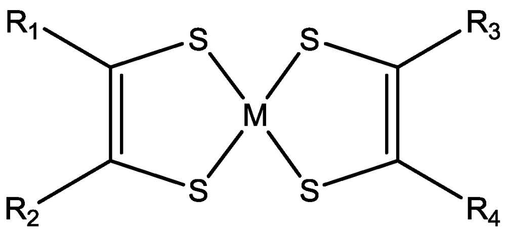


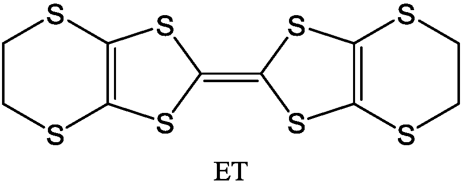
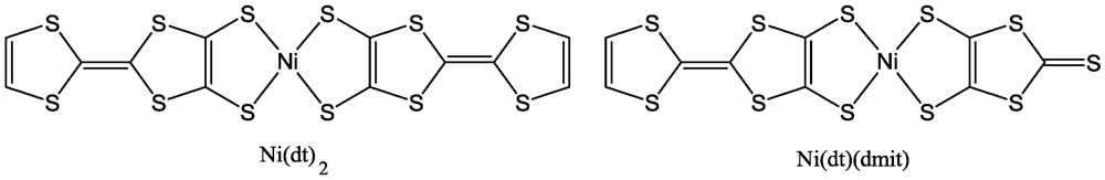


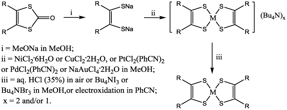
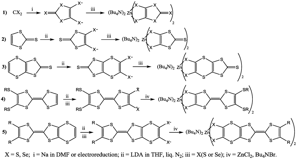
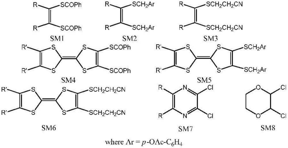

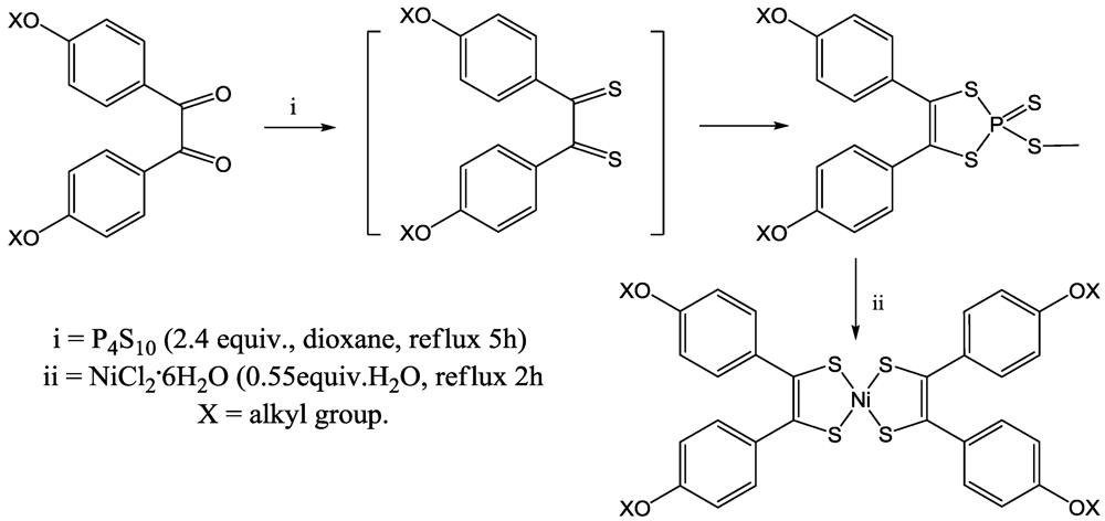

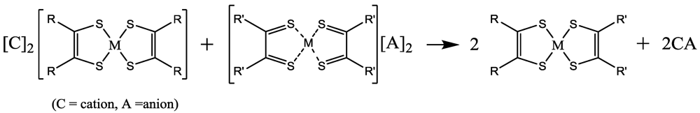
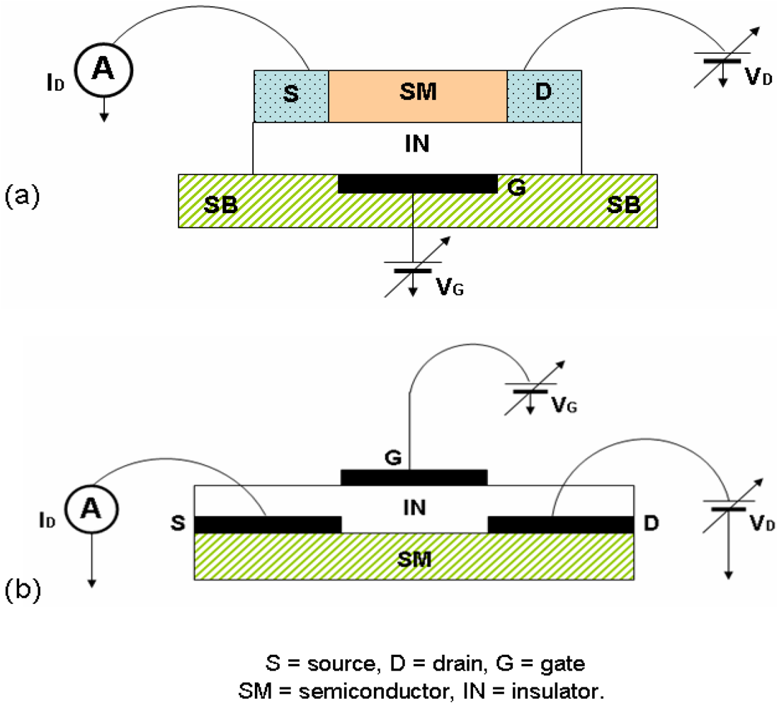
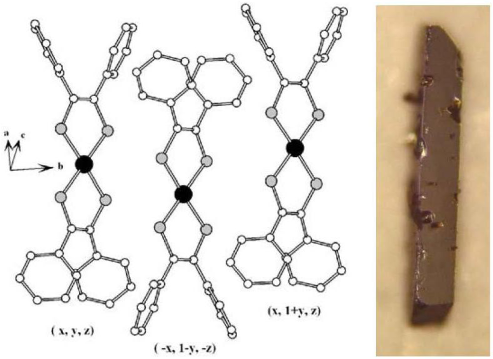
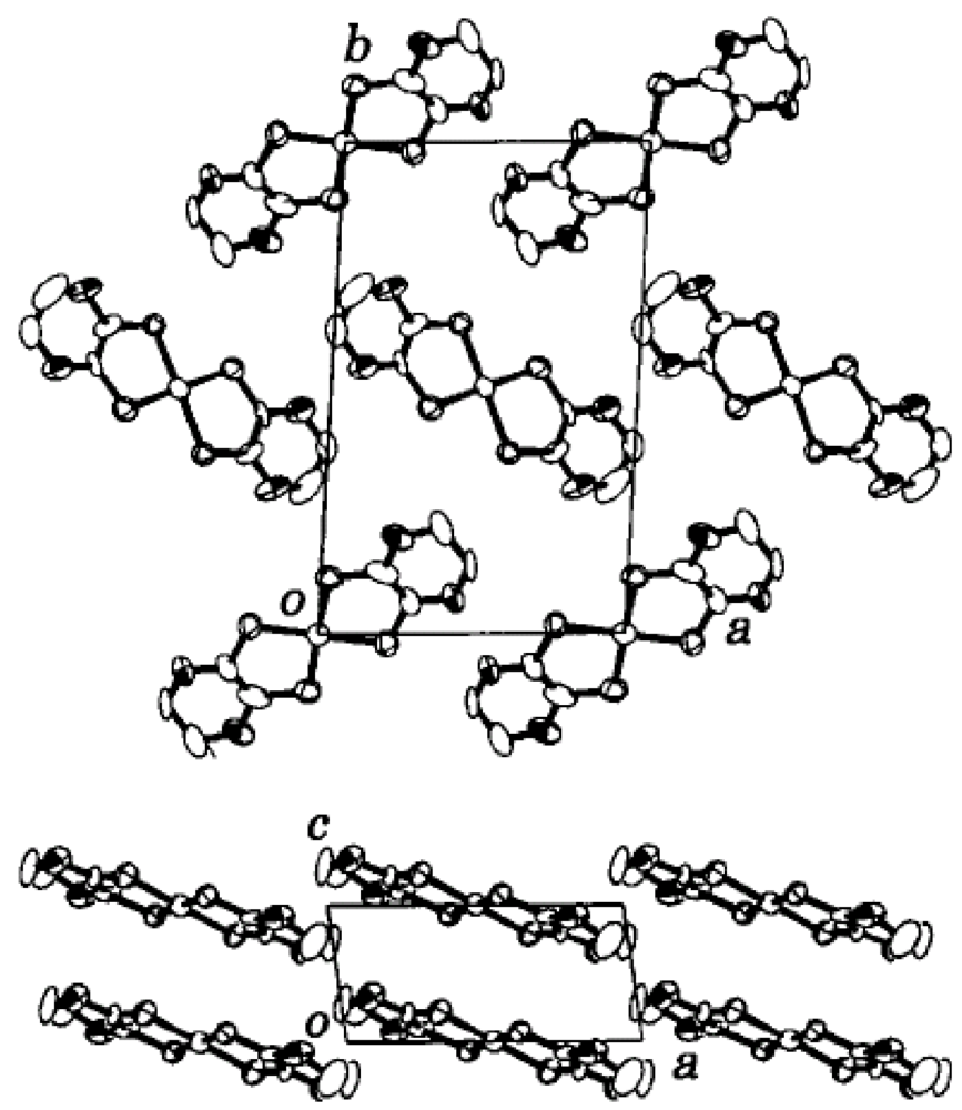

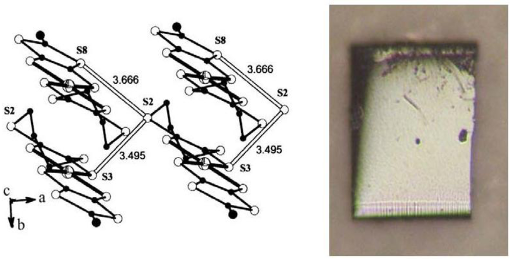
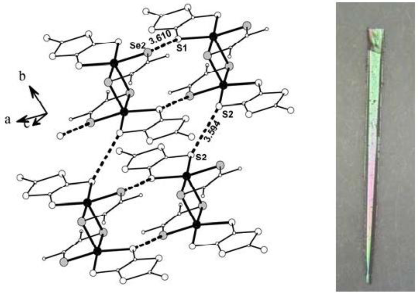
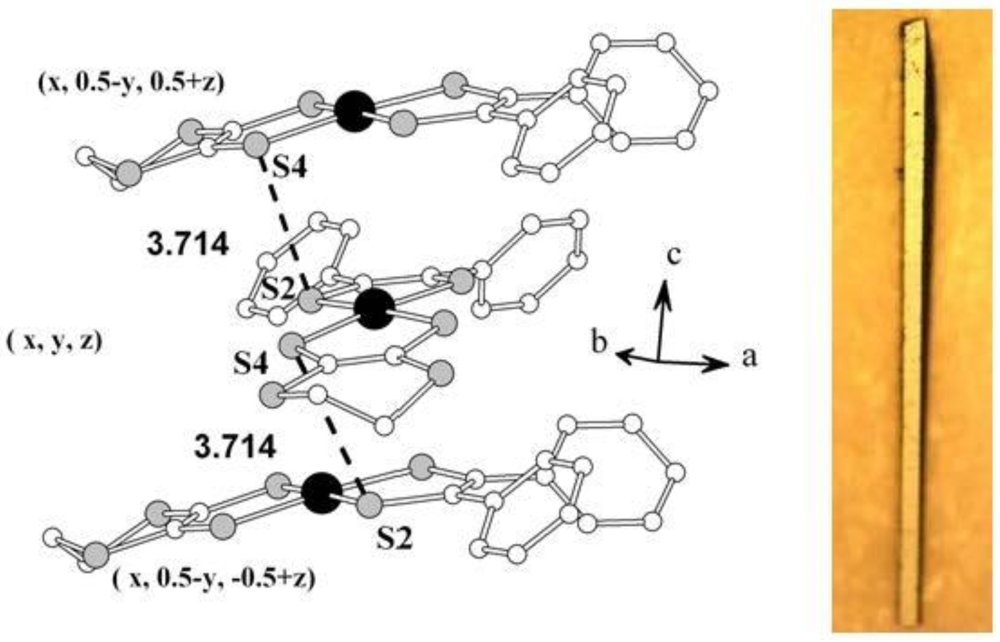
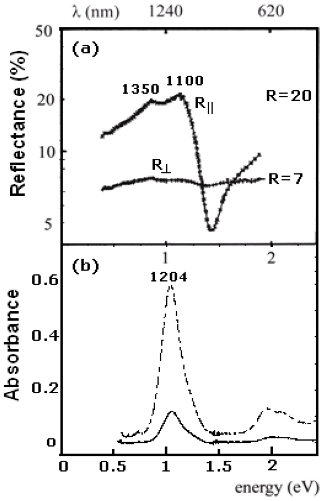
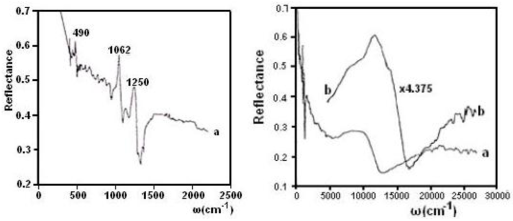
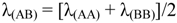 (1)
(1) 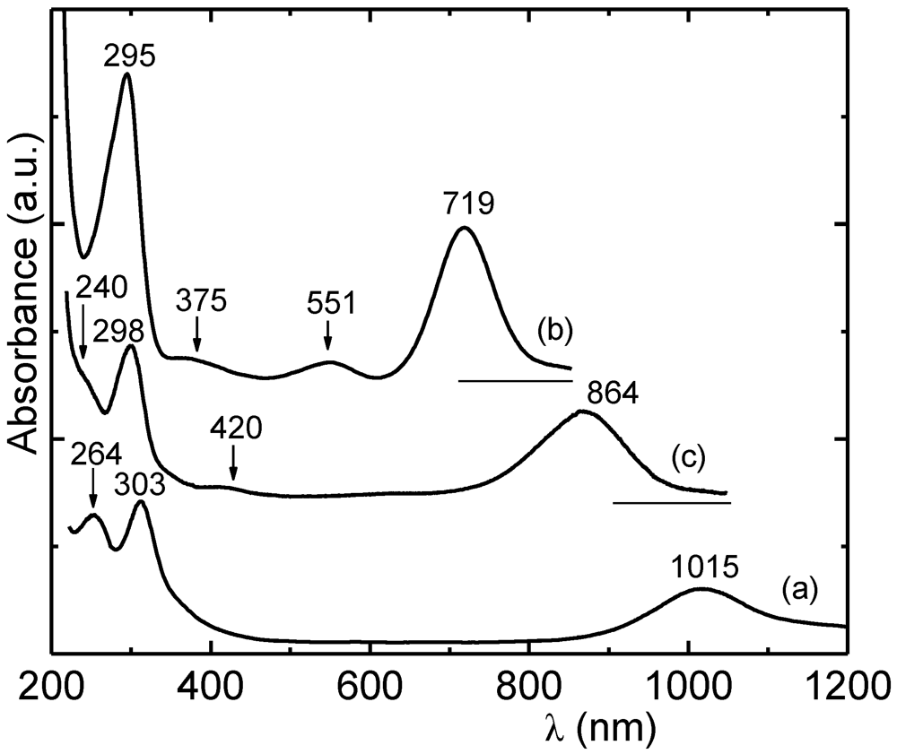

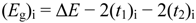 (2)
(2) 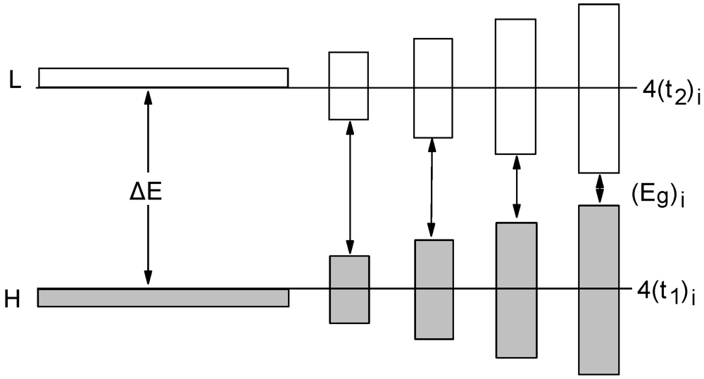


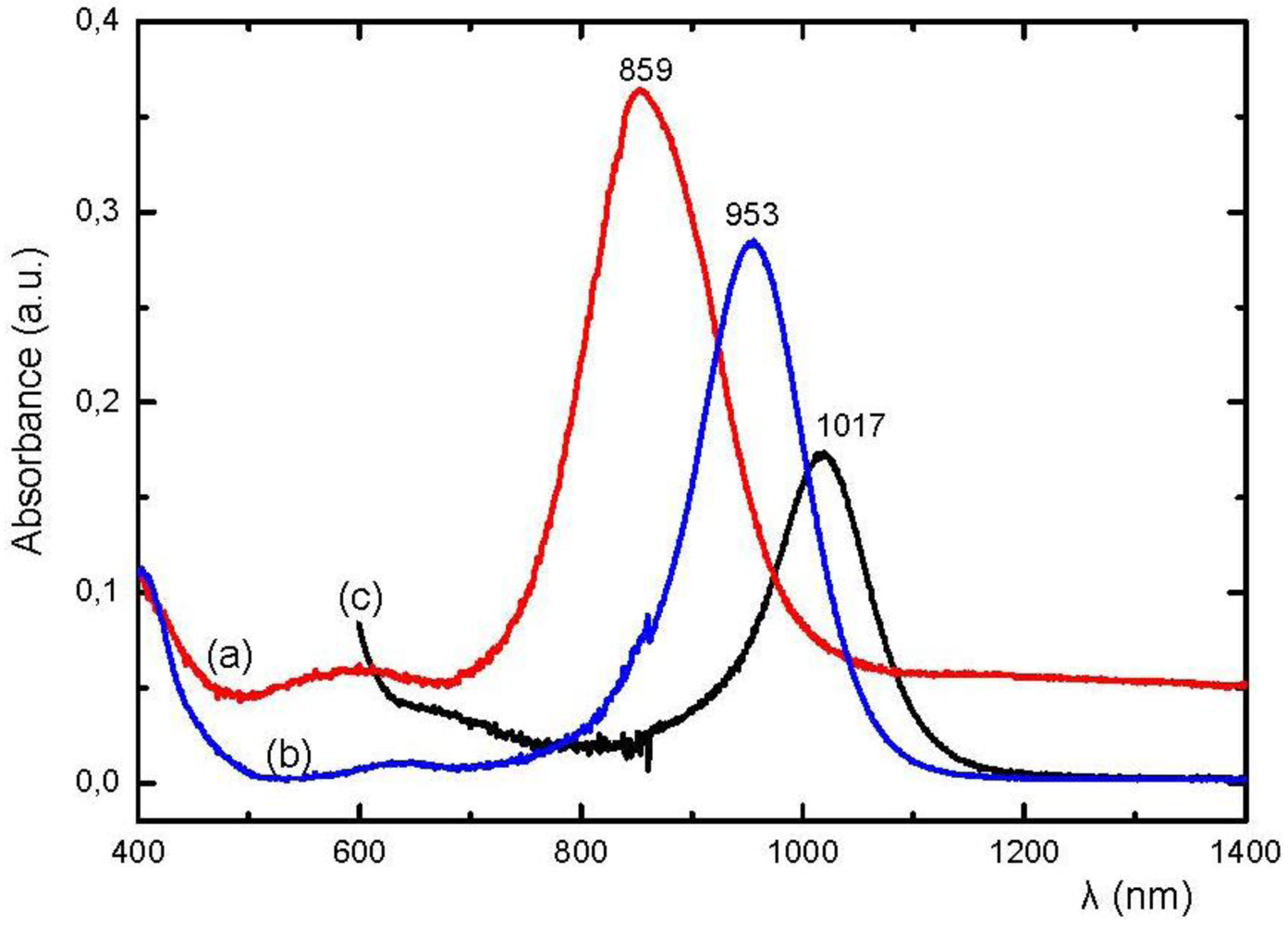
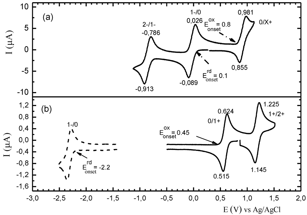
 (3)
(3) (4)
(4)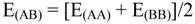 (5)
(5)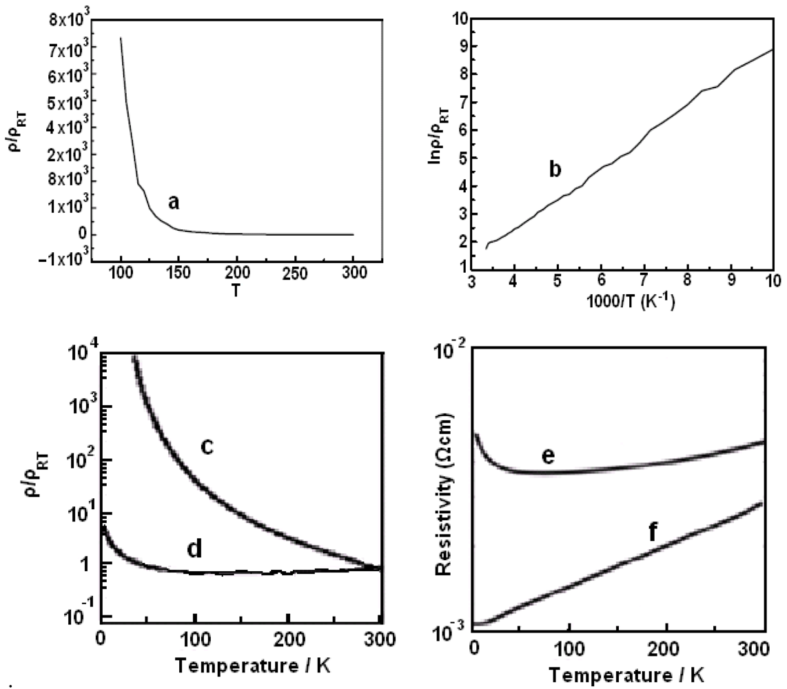
 (6)
(6)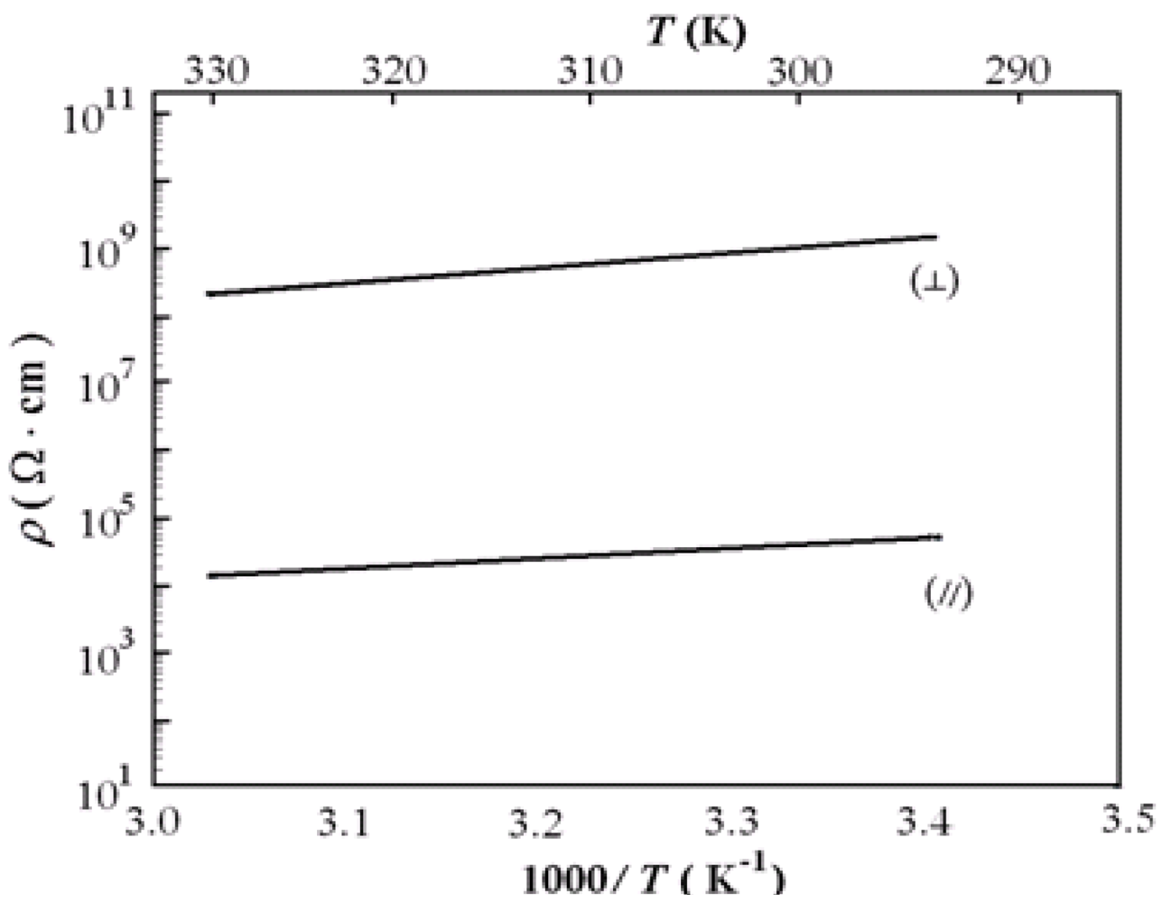
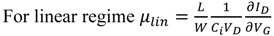 (7)
(7) (8)
(8)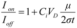 (9)
(9)
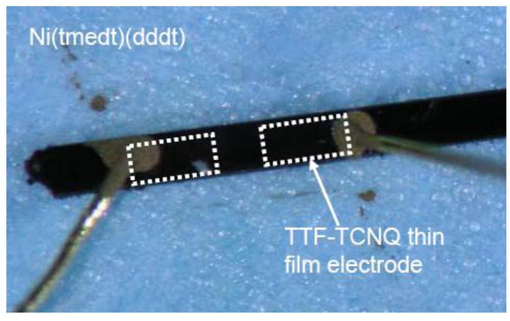
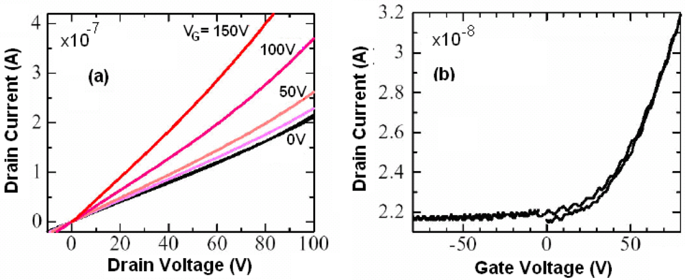

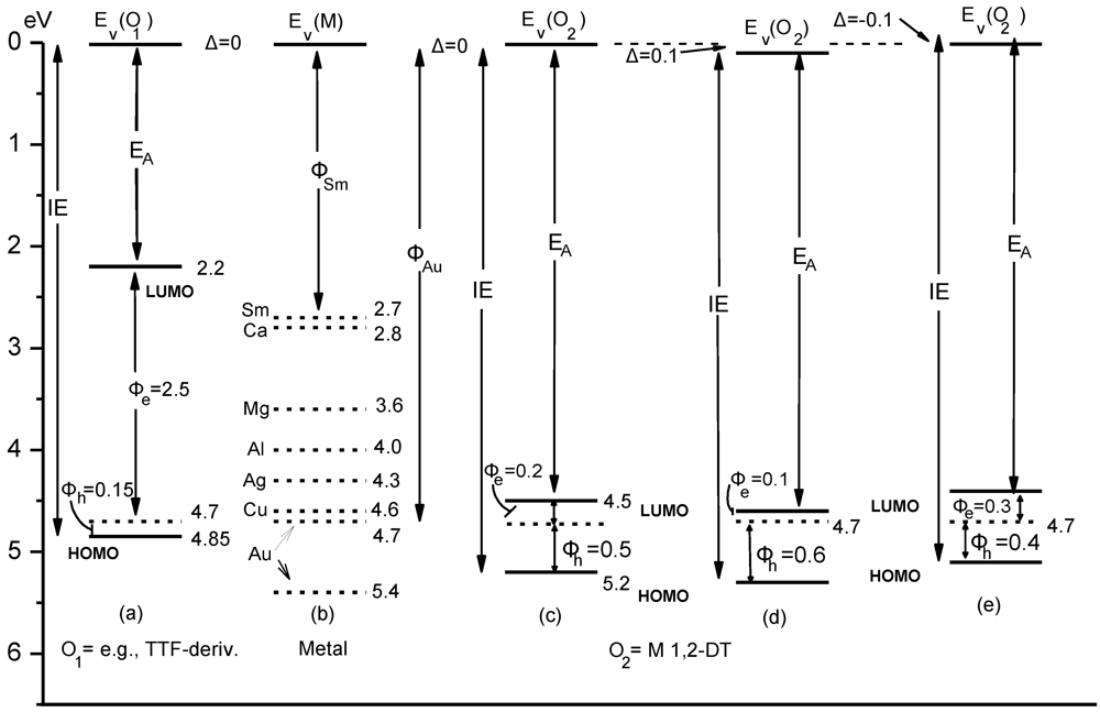
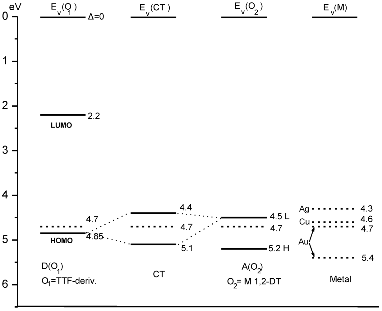
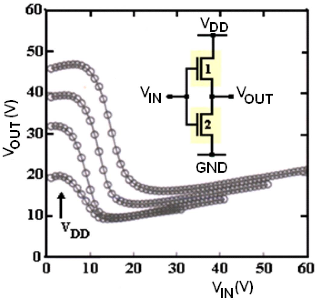
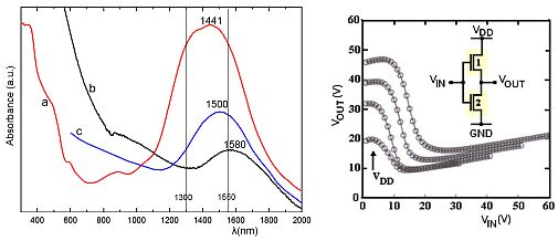
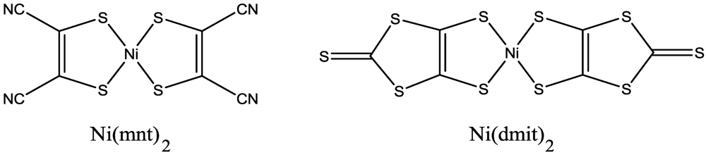
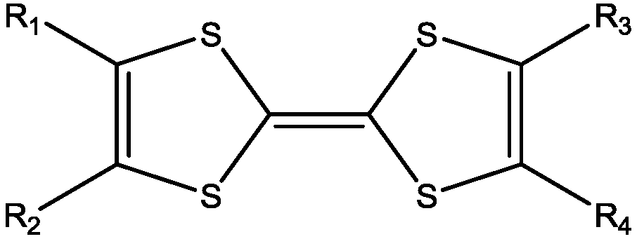
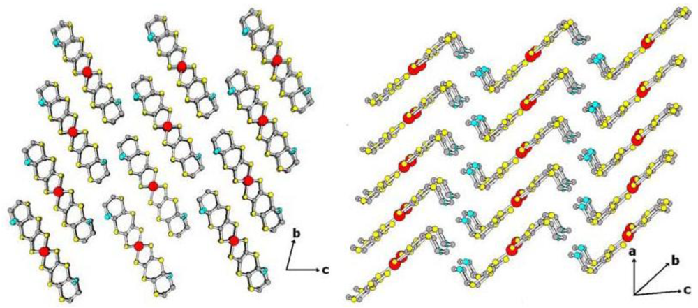
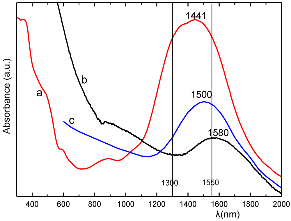
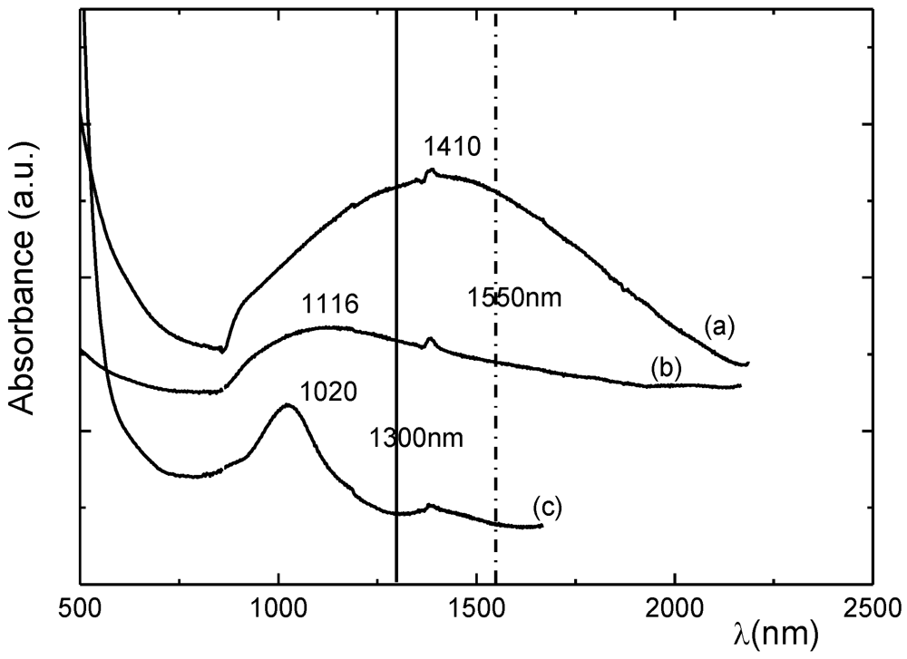
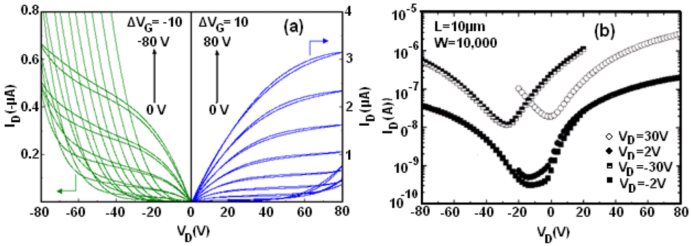
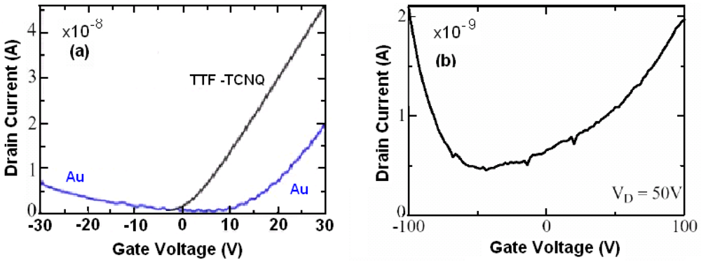