Article

Electronic Structure and Optical Properties of Cu2ZnSnS4 under Stress Effect

College of Physics and Electronic Science, Anshun University, Anshun 561000, China
*
Author to whom correspondence should be addressed.
Crystals 2022, 12(10), 1454; https://doi.org/10.3390/cryst12101454
Submission received: 27 September 2022 / Revised: 6 October 2022 / Accepted: 10 October 2022 / Published: 14 October 2022
(This article belongs to the Special Issue Crystallization of High Performance Metallic Materials)

Abstract

:
By using the pseudopotential plane-wave method of first principles based on density functional theory, the band structure, density of states and optical properties of Cu2ZnSnS4 under isotropic stress are calculated and analyzed. The results show that Cu2ZnSnS4 is a direct band gap semiconductor under isotropic stress, the lattice is tetragonal, and the band gap of Cu2ZnSnS4 is 0.16 eV at 0 GPa. Stretching the lattice causes the bottom of the conduction band of Cu2ZnSnS4 to move toward lower energies, while the top of the valence band remains unchanged and the band gap gradually narrows. Squeezing the lattice causes the bottom of the conduction band to move toward the high-energy direction, while the top of the valence band moves downward toward the low-energy direction, and the Cu2ZnSnS4 band gap becomes larger. The static permittivity, absorption coefficient, reflectivity, refractive index, electrical conductivity, and energy loss function all decrease when the lattice is stretched, and the above optical parameters increase when the lattice is compressed. When the lattice is stretched, the optical characteristic peaks such as the dielectric function shift to the lower-energy direction, while the optical characteristic peak position shifts to the higher-energy direction when the lattice is compressed.

1. Introduction

With the increasing scarcity of non-renewable energy sources such as fossils, the energy crisis and environmental pollution problems are becoming more and more prominent. The development of new energy sources, such as solar energy and wind energy, is an effective means to solve the energy crisis and environmental pollution problems [1]. Among many new energy sources, solar energy has received great attention due to its advantages of greenness, environmental protection, and high efficiency [2,3,4,5,6]. Solar cells are the main means of utilizing solar energy. Solar cells include silicon-based solar cells, perovskite solar cells, organic solar cells, dye-sensitized cells, compound thin-film solar cells, etc. [7,8,9,10,11]. Compound thin-film solar cells are effective devices for utilizing solar energy due to their small size, light weight, and flexibility. Compound thin-film solar cells mainly include [12,13,14] CdTe cells, GaAs cells, Cu(In-Ga)(Se,S)2 cells, and so on. Among them, Cu(In-Ga)(Se,S)2 cellshavehigh battery conversion efficiency due to their spike-like conduction band valence and they do not damage the short-circuit current [15] and are widely used. Cu(In-Ga)(Se,S)2 cells contain rare metals In and Ga, which are limited in large-scale commercial applications. Therefore, seeking environmentally friendly solar cell materials is one of the strategies to solve the difficulty of the large-scale application of Cu(In-Ga)(Se,S)2 cells. The band gap of the semiconductor material Cu2ZnSnS4 (CZTS) is 1.4~1.6 eV, which is strongly matched with the required band gap of the solar cell absorber material [16]. The physical and chemical properties of CZTS are very close to those of Cu(In-Ga)(Se,S)2. The theoretical conversion efficiency of CZTS as an absorber layer of solar cells is 32.2% [17], and CZTS is rich in various elements in the crust, as well as being non-toxic and non-polluting. Therefore, CZTS is considered as a high-efficiency, low-cost, and environmentally friendly solar cell material.
At present, the experimentally reported value of the conversion efficiency of CZTS solar cells reaches 12.6% [18], but there is still a large gap between this and the theoretical calculation value, and the conversion efficiency of the cell has large room for improvement. The main factors affecting the conversion efficiency of CZTS solar cells are the low open-circuit voltage Voc and low filling factor of the cell [19,20]. Since the ionic radii of Cu and Zn are very close, substitution defects of Cu and Zn are easily formed in the CZTS system. Anti-occupancy defects with Cu and Sn and Zn anti-occupancy defects [21] will introduce energy level defects to different degrees and inhibit the open-circuit voltage Voc of the battery. It was found [22] that the introduction of metal ions in CZTS can play a role in the passivation of defects; for example, the introduction of a small amount of Ge can suppress intrinsic deep-level SnZn defects. We note that the doping of monovalent metals such as silver can change the defects of Cu2ZnSnS4, thus adjusting the band gap. Due to the high formation energy of AgZn defects, when the Ag doping concentration is high, the defect concentration of the CZTS system is low, which is conducive to increasing the carrier concentration. Affected by the electronic configuration of elements, the atomic radii of Ag atoms and Cu atoms differ greatly, which causes the bending coefficient of the energy band to change. Low-concentration doping causes the energy band to change slowly, while high-concentration doping causes the energy band to change obviously [23].
In addition, the introduction of stress into the material can play the role of changing the lattice constant, regulating the energy band structure, and changing the optical properties. The 4-metal alloy of Cu2ZnSnS4 is derived from the binary alloy of ZnS [24]; due to its good band gap matching and strong light absorption, it is an ideal solar cell absorption layer material. However, CuZn and SnZn defect energy levels exist when Cu2ZnSnS4 alloy films are actually prepared, which affects the photoelectric properties of the materials. Therefore, we control the band gap and photoelectric properties of Cu2ZnSnS4 alloy films by applying stress. Stressing is an effective means to regulate the heterojunction carrier dynamics [25]. As a solar cell absorbing layer material, CZTS needs to form a solar cell system together with other materials, so it is necessary to consider the transport of electrons and holes at the heterojunction interface. Adjusting the stress can change the K point energy level of the material. When the K point energy level is coupled with other energy levels, it can provide an intermediate-state energy level for electron and hole transfer, making the transfer of electrons and holes between layers easier, and improving the utilization of photogenerated carriers. In addition, adjusting the stress can change the orbital occupancy of electrons, thereby changing the photoelectric characteristics of the film. At the same time, adjusting the stress can also change the phase transition temperature of the film [26]. Therefore, it can be predicted that the introduction of stress is an effective means to adjust the photoelectric properties and phase transition temperature of CZTS. Based on the above considerations, we study the effect of stress on the electronic structure and optical properties of CZTS.
There have been extensive reports on the photoelectric properties of materials by introducing stress [27,28,29,30]. However, there are few reports on the effect of stress on the electronic structure and optical properties of CZTS. In this paper, by using the pseudopotential plane-wave method of first principles based on density functional theory, the band structure, density of states, and optical properties of Cu2ZnSnS4 under isotropic stress are calculated and analyzed.

2. Methods and Calculations

The calculation model selected in this paper is Cu2ZnSnS4 with a kesterite structure, the space group is I 4 ¯ ( N o .82 ) , the lattice constants are a = b = 0.54628 nm, c = 1.0864 nm, and the crystal plane angle is α = β = γ = 90° [31]. The unit cell structure of Cu2ZnSnS4 is shown in Figure 1.
The first-principles-based pseudopotential method was used for the calculations; all calculations were performed using the Cambridge Serial Total Energy Package (CASTEP) [32] in Materials Studio software, and processed using the Perdew–Burke–Eurke–Ernzerh(PBE) [33] functional of the generalized gradient approximation (GGA) for the exchange correlation energy between electrons. An ultrasoft pseudopotential [34] was used to deal with the interaction between ionic solids and electrons. The truncation energy was set to 400 eV, the self-consistent convergence accuracy was 1.0 × 10⁻⁷ eV/atom, and the integral of the Brillouin zone was divided by 5 × 5 × 2 of Monkhorst–Pack.

3. Results and Discussion

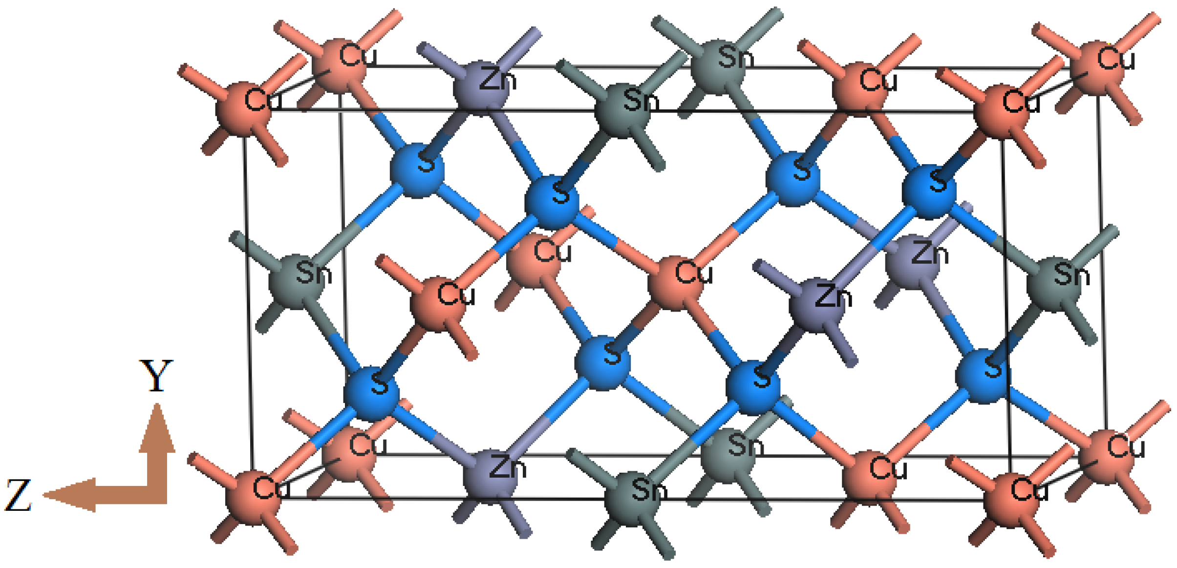
3.1. Geometry Optimization

Table 1 shows the lattice constants of Cu2ZnSnS4 with a kesterite structure obtained after applying isotropic tensile stress and compressive stress optimization, where “−” represents tensile stress. It can be seen from Table 1 that with the increase inisotropic tensile stress, the lattice constant of CZTS increases, the volume of the unit cell increases, and the lattice of CZTS is tetragonal. With the increase inisotropic compressive stress, the lattice constant of CZTS decreases, the unit cell volume decreases, and the lattice still maintains the tetragonal system. The results calculated by us are in good agreement with those of Liu [35], which shows that the applied stress has a significant effect on the lattice constant and cell volume of Cu2ZnSnS4.
For comparison, the theoretical calculations [36] and experimental values [37] of lattice constant and cell volume are added in Table 1. It can be seen from Table 1 that when no stress is applied, the difference between the a and b values and theoretical calculation is 0.0%, and the difference between them and the laboratory values is 0.7%. The difference between the c value and theoretical calculation is 0.2%, and the difference between the c value and experimental value is 0.8%. The unit cell volume is 0.2% different from the theoretical calculation and 2.4% different from the experimental value. The results in Table 1 show that our calculation results are in good agreement with the calculation and experimental values of other research groups.

3.2. Electronic Structure

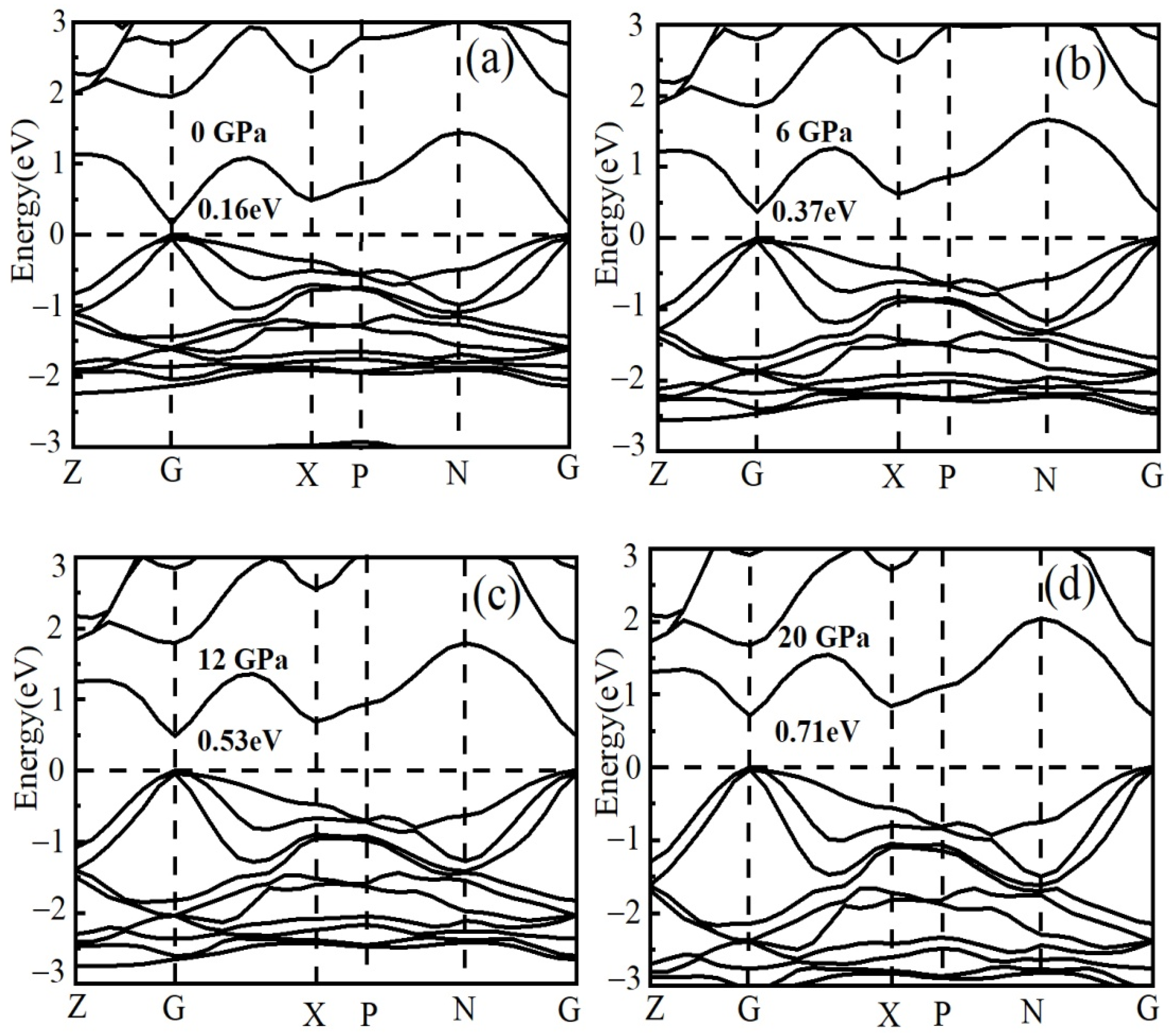
3.2.1. Band Structure

Figure 2 shows the Cu2ZnSnS4 band structure obtained by applying tensile stress. It can be seen from the figure that CZTS is a typical direct band gap semiconductor, and the minimum band gap value is obtained at the highly symmetrical G point position. The band gap of CZTS is 0.16 eV when no stress is applied (0 GPa), which is consistent with the research results of Zhao [38].
With the increase intensile stress, the bottom of the conduction band moves to the lower-energy direction, while the top of the valence band remains unchanged; the band gap decreases with the increase intensile stress, and the band gap reaches a minimum value of 0.02 eV when the tensile stress is −4 GPa. After this, the band gap widens with the increase intensile stress. This is because the bottom of the conduction band of CZTS moves toward the high-energy direction after the tensile stress continues to increase, while the top of the valence band moves down toward the low-energy direction, and the band gap widens.
Figure 3 shows the band structure of Cu2ZnSnS4 obtained by applying compressive stress. It can be seen from Figure 3 that the CZTS is still suitable as a direct bandgap semiconductor; the minimum bandgap value is still obtained at the highly symmetrical G point position.
With the increase incompressive stress, the bottom of the conduction band of CZTS moves towards high energy and the top of the valence band remains unchanged. The band gap of CZTS widens with the increase incompressive stress. When the applied compressive stress is 20 GPa, the band gap of CZTS reaches 0.71 eV.

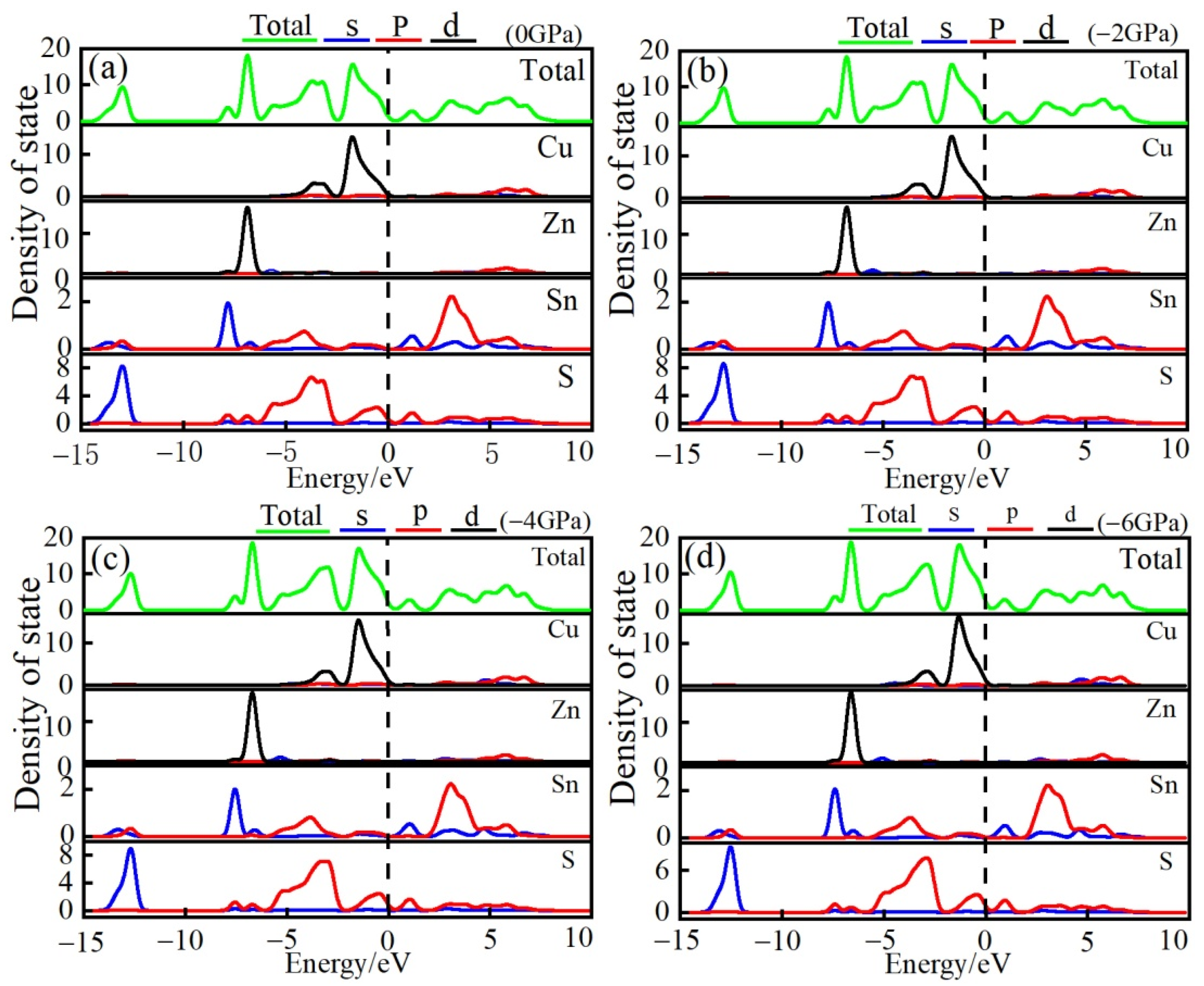
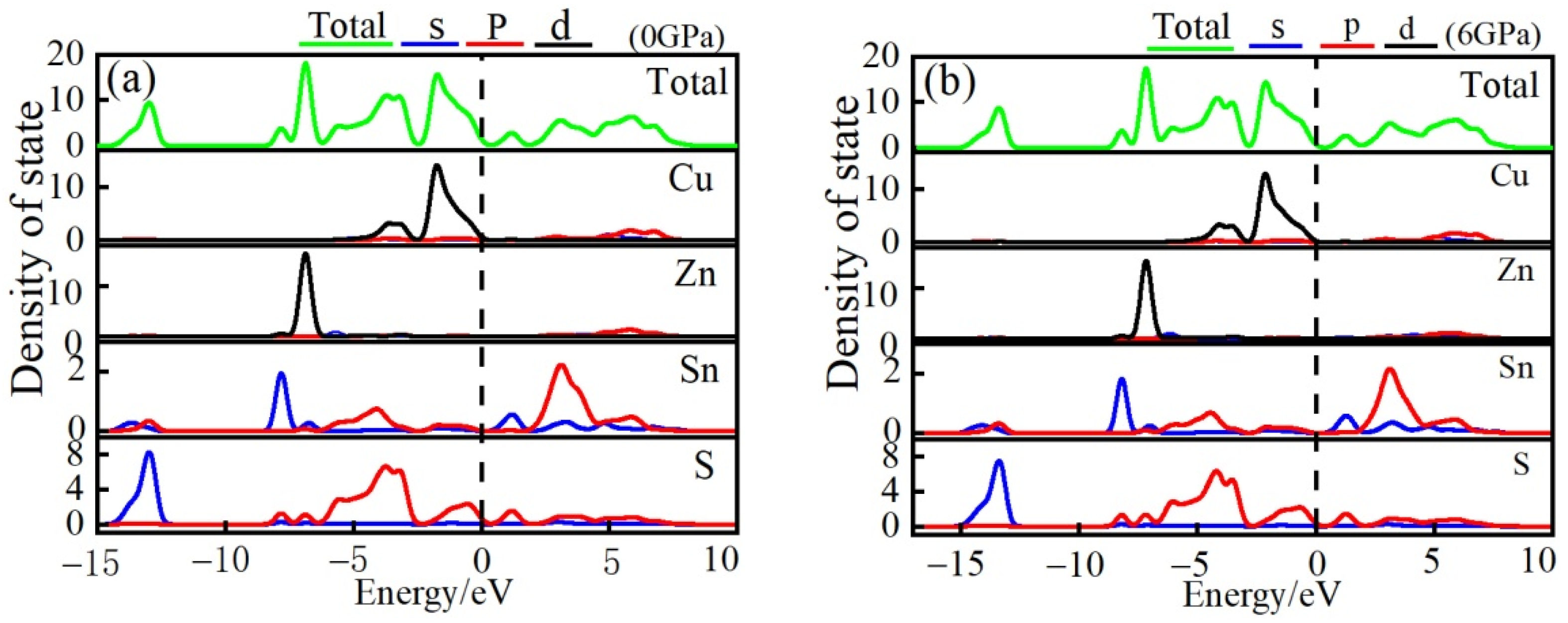
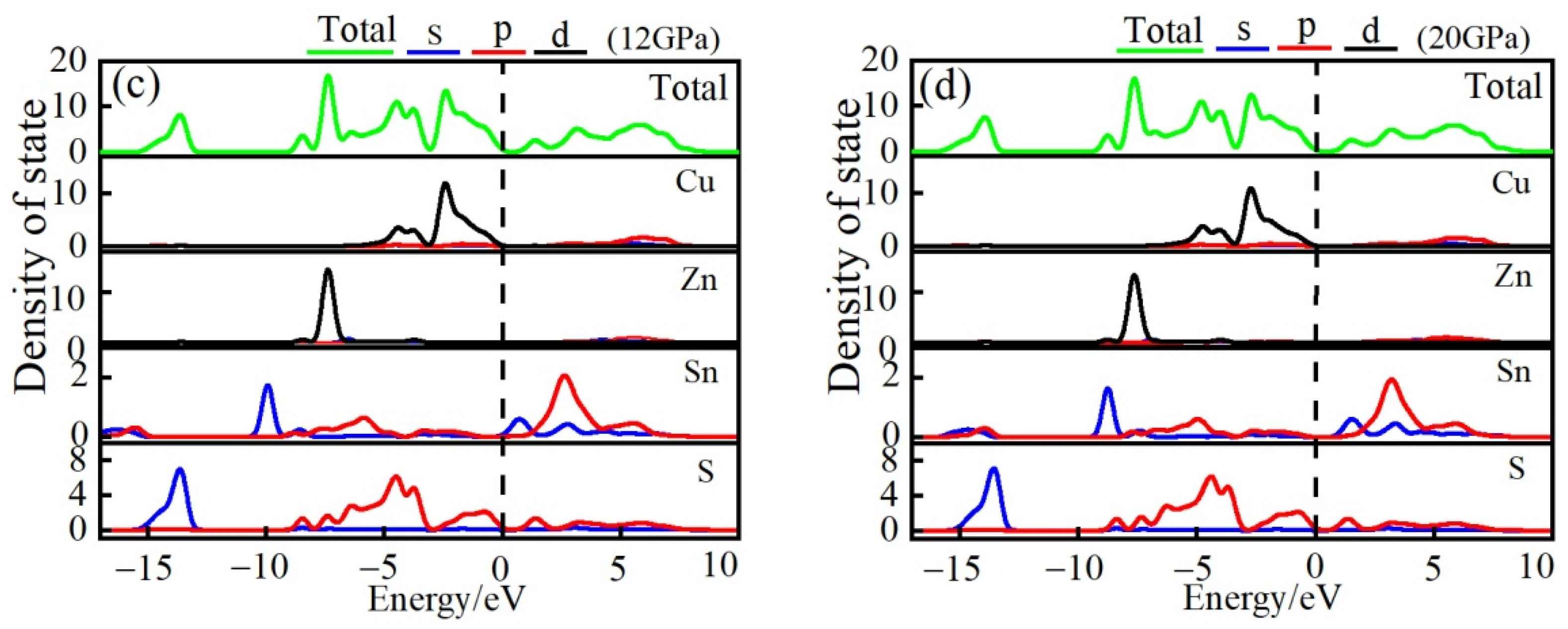
3.2.2. Density of Electronic States

The total density of states and the density of states of each atomic partial wave under the action of tensile stress are shown in Figure 4. The main contributions to the CZTS density of states are the Cu 3d configuration, Zn 3d configuration, Sn 5s and 5p configuration, and S 3s and 3p configuration, and the 3p configuration of Cu and Zn also has a small contribution.
It can be seen from Figure 4 that the lower valence band region of −14.5~−12.3 eV is mainly contributed by the 3s state of S and a small amount of 5p state electrons of Sn. The mid-valence band region of −8.4~−5.5 eV is mainly contributed by the 3d state of Zn, the 5s state of Sn, and a small amount of the 3p state of S and 4s state of Zn. The upper valence band region of −5.5~0 eV is mainly contributed by the 3d state of Cu, a small amount of the Sn 5p state, and the 3p state of S. The conduction band part is mainly contributed by the 5s and 5p states of Sn and a small amount of the 3p state of S.
With the increase intensile stress, the peak position of the density of states in the valence band of CZTS shifts to the higher-energy direction. The −13 eV peak is shifted to the high-energy band by 0.45 eV, the −6.88 eV peak is shifted to the high-energy band by 0.27 eV, the −3.69 eV peak is shifted to the high-energy band by 0.8 eV, and the −1.73 eV peak is shifted to the high-energy band by 0.42 eV. The peak position of the conduction band is shifted to the lower-energy direction, and the shift amount is essentially the same at around 0.13 eV.
The Cu2ZnSnS4 density of states and the partial wave density of states under the action of compressive stress are shown in Figure 5.
It can be seen from Figure 5 that the electronic configurations contributing to the valence and conduction bands of CZTS are essentially the same as those under tensile stress. The peak positions of the density of states in the valence band of CZTS shifted to the lower-energy direction with the increase in compressive stress, with an average offset of 0.64 eV, and the peak positions of the density of states in the conduction band shifted to the high-energy direction with an average offset of 0.17 eV.
We believe that when the lattice is subjected to tensile stress, the interatomic distance increases, the coupling degree of valence electrons decreases, the electrostatic repulsion decreases, the attractive force between valence electrons near the Fermi level and electrons in the conduction band increases, and some valence electrons break free. The tendency for nuclear confinement to occupy higher energy levels becomes more pronounced with increasing tensile stress.
Since valence electrons occupy higher energy levels, the energy required for their transition to the conduction band decreases and the band gap narrows. On the contrary, when the lattice is subjected to compressive stress, the atomic spacing decreases, the coupling degree of valence electrons increases, and the electrostatic repulsion increases, which hinders valence electrons from occupying high-energy states and pushes valence electrons to move to lower-energy orbitals. Therefore, the energy required for the transition of valence electrons to the conduction band increases, and the band gap becomes wider.
On the other hand, when the material is stressed, the Coulomb force changes due to the change in atomic spacing. These changes lead to an increase or decrease in exciton binding energy [39], which affects the dielectric shielding effect and ultimately affects the electron transport, making the band gap wider or narrower.

3.3. Optical Properties

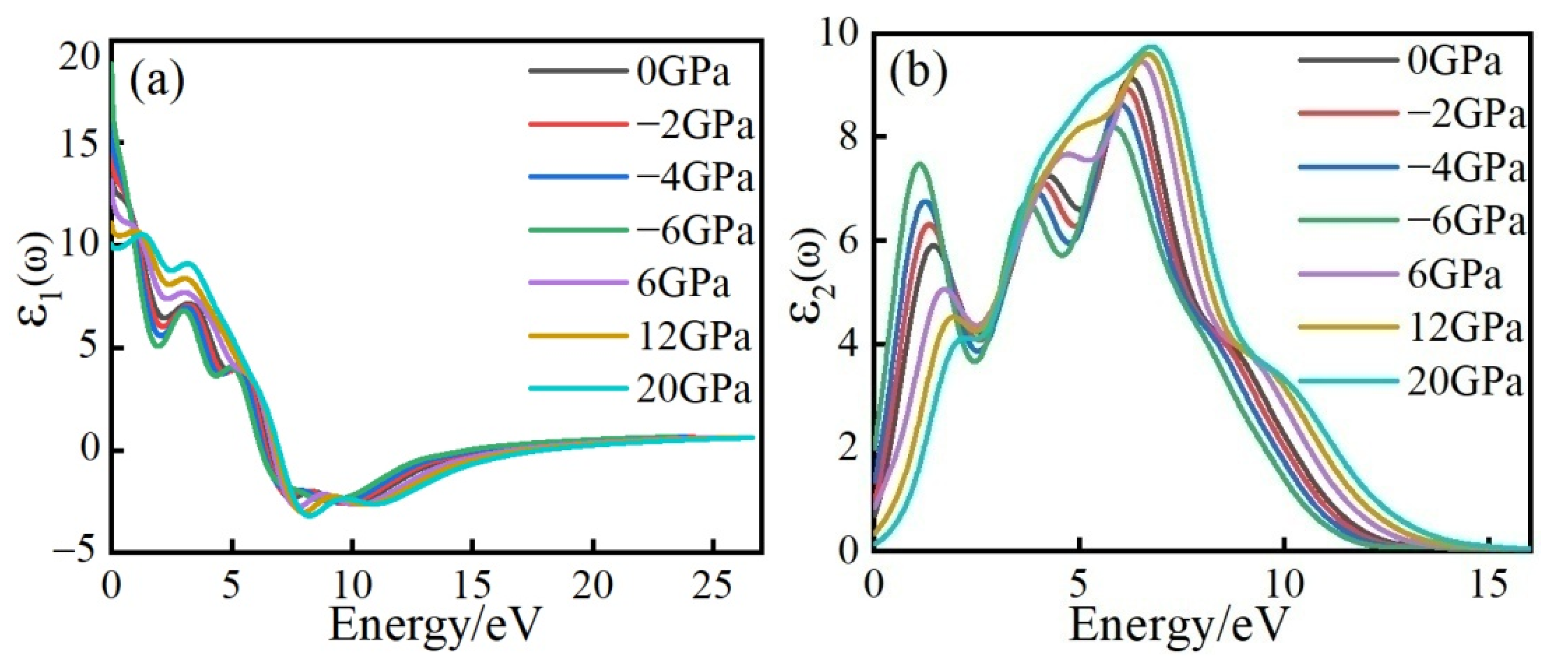
3.3.1. Complex Dielectric Function

The dielectric function ε ( ω ) = ε 1 ( ω ) + i ε 2 ( ω ) is a complex number. The imaginary part ε 2 indicates that the polarization of the molecules inside the material cannot keep up with the change in the external electric field; it represents the loss. The real part ε 1 indicates the ability of the material to bind charges. The dielectric function reflects the band structure of the solid and its spectral information [40], and the dielectric peak of the dielectric function is mainly determined by the band structure and density of states. Figure 6 is a graph showing the change in the CZTS real part ε 1 and imaginary part ε 2 with photon energy under stress.
It can be seen from Figure 6a that when the tensile stress is 0, −2, −4, and −6 GPa, the corresponding static dielectric constants are 13.74, 14.98, 16.48, and 18.88. When the compressive stress is 6, 12, and 20 GPa, the corresponding static dielectric constants are 13.09, 11.09, and 10.04. It can be seen from the figure that the static permittivity of CZTS increases when the lattice is subjected to tensile stress, while the static permittivity of CZTS decreases when it is subjected to compressive stress. At 0 GPa, the imaginary part of the complex dielectric function of CZTS has four distinct characteristic peaks at 1.44, 4.23, 6.26, and 8.58 eV. Combining the density of states in Figure 4a, it can be seen that the dielectric peak at 1.44 eV has mainly transitioned from Cu 3d orbital electrons to Sn 5s orbital electrons, and the dielectric peak at 4.23 eV has mainly transitioned from Cu 3d orbital electrons to Sn 5p orbital electrons, at 6.26 eV. The dielectric peak at 8.58 eV mainly transitions from Cu 3d orbital electrons to Sn 5p orbital electrons, and the dielectric peak at 8.58 eV mainly transitions from Zn 3d orbital electrons to Sn 5s orbital electrons. When the energy is lower than 3.78 eV, the dielectric peak shifts to the high-energy direction with the increase instress, and the peak decreases with the increase instress. When the energy is greater than 3.78 eV, the dielectric peak also shifts to the high-energy direction with the increase instress, but, at this time, the peak increases with the increase instress. As the stress increases, the CZTS band gap increases, so the dielectric peak shifts toward higher energies. The above conclusions are consistent with the results of the literature [41]; this is in agreement with the relation between the band gap energy and the dielectric response, which implies that the larger band gap energy results in a small dielectric constant.

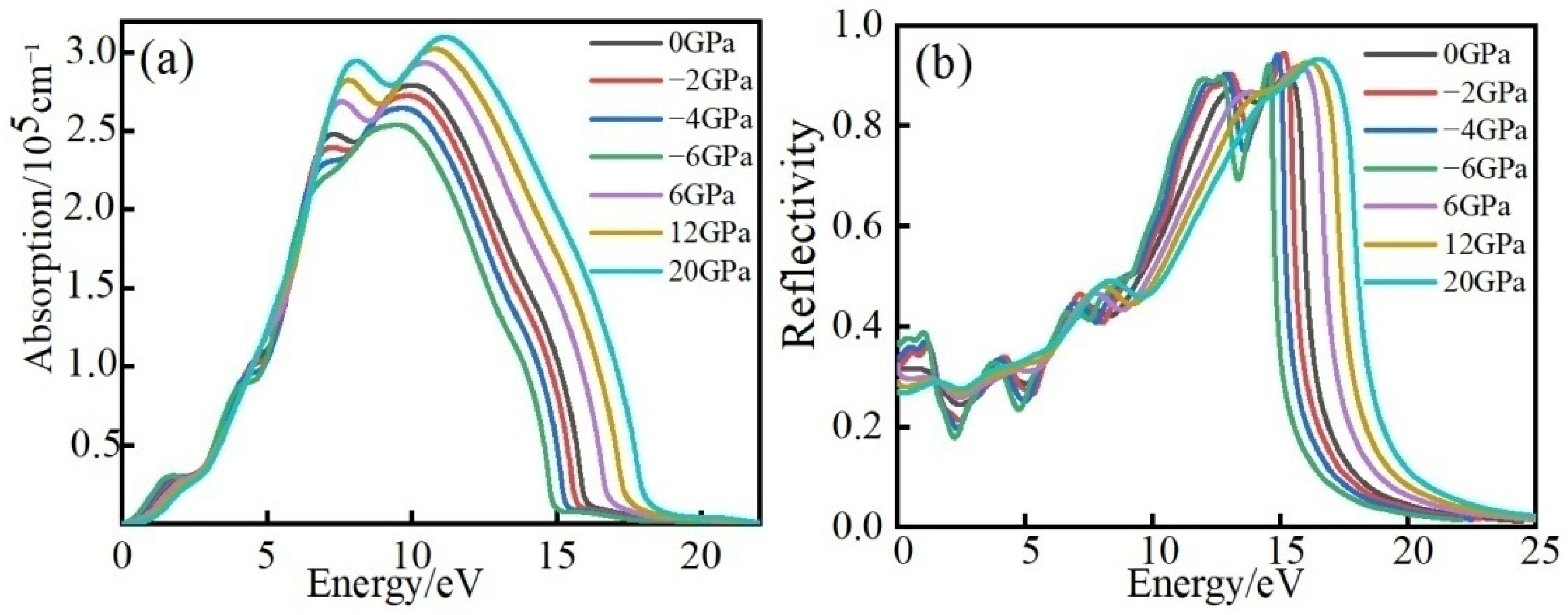
3.3.2. Absorption and Reflection Spectra

The absorption spectrum of Cu2ZnSnS4 is shown in Figure 7a. It can be seen from the figure that the absorption spectrum of CZTS is mainly divided into three parts: the visible light region of 0.5~4.8 eV, the ultraviolet light absorption region of 4.8~14.2 eV, and the absorption range of more than 14.2 eV in the high-energy absorption area. In the range of 0.5~9.9 eV, the absorption coefficient gradually increased with the increase in incident light energy, and the light absorption decreased sharply when the energy was greater than 9.9 eV, while CZTS almost no longer absorbed the spectrum when the energy was greater than 16.19 eV. It can be seen from the figure that the absorption coefficient of CZTS in the visible light band is greater than 104 cm−1 [42], and the light absorption is good.
With the increase incompressive stress, the absorption peak of CZTS shifted to the high-energy direction, and the peak value gradually increased. With the increase intensile stress, the absorption peak of CZTS shifted to the lower-energy direction, and the peak value gradually decreased. The results obtained in this paper are very consistent with the research results of Kahlaoui [43], and the phenomena could be attributed to the decrease in the electronic transition energy with the strain, which results in more photons being absorbed.
In this work, it is believed that when the lattice is subjected to tensile stress, the atomic spacing becomes larger, and the light wave of the same energy is "short-wave" relative to the lattice, the lattice scattering effect is enhanced, and the light absorption is weakened. In contrast, when the lattice is subjected to compressive stress, the atomic spacing decreases, and the light wave with the same energy is "long-wave" relative to the lattice, the lattice scattering effect is weakened, and the light absorption is enhanced.
Figure 7b shows the reflectance spectrum of CZTS. The reflectance in the visible light region of 0.5~4.8 eV is lower than 30%, indicating that CZTS has good light absorption in the visible light region. With the increase in incident light energy, the reflectivity gradually increased and reached a peak value of 90% near 15.30 eV, and high reflectivity appeared in the ultraviolet and high-energy regions. As the compressive stress increases, the reflection peak shifts towards higher energy. However, as the tensile stress increases, the reflection peak shifts toward the lower-energy direction.

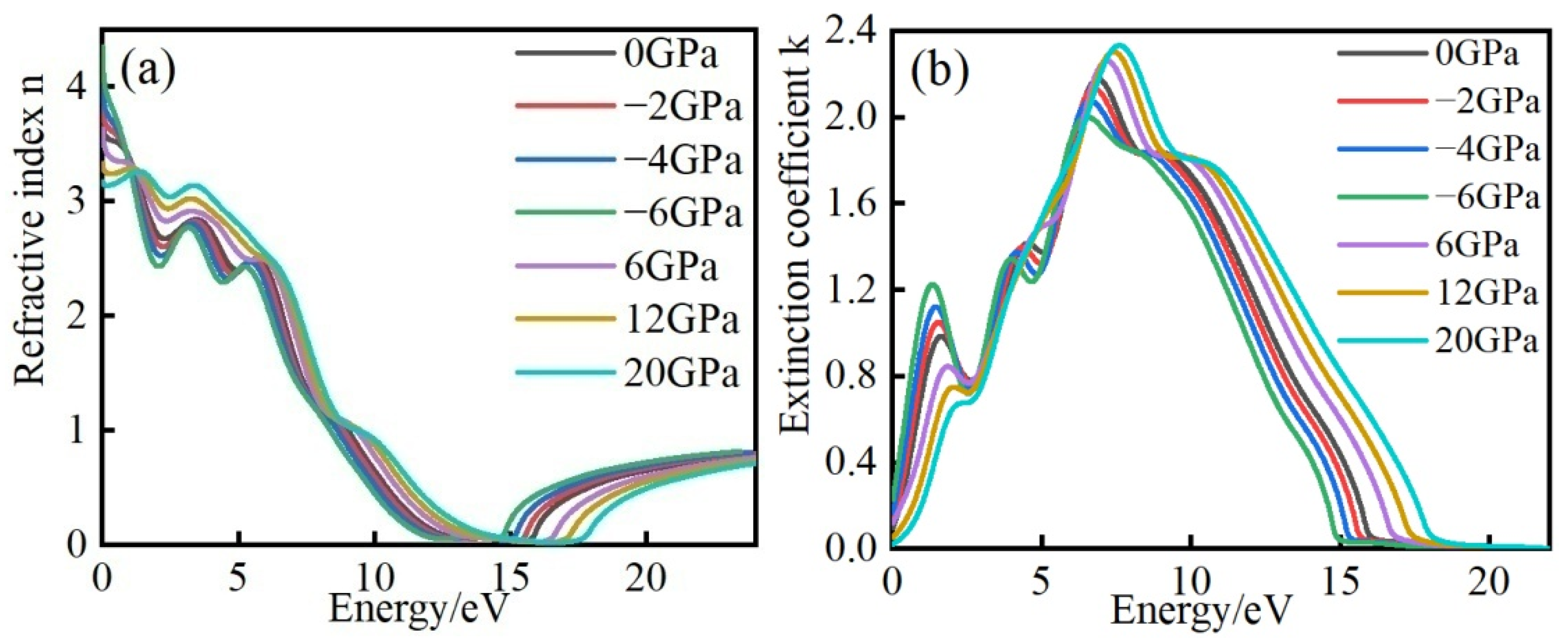
3.3.3. Complex Refractive Index

Figure 8 shows the Cu2ZnSnS4 complex refractive index; (a) is the refractive index, and (b) is the extinction coefficient.
It can be seen from Figure 8 that when the energy is greater than 16 eV, the refractive index is essentially constant, and the extinction coefficient is around 0, indicating that the absorption of CZTS is weak at high frequencies, which is consistent with the conclusion of the absorption spectrum. It can also be seen from the figure that the refractive index decreases with increasing tensile stress and increases with increasing compressive stress. This is mainly because the unit cell volume becomes larger when tensile stress is applied, the density becomes worse, and the refractive index decreases. When compressive stress is applied, the volume of the unit cell decreases, the density of CZTS becomes better, and therefore the refractive index increases.

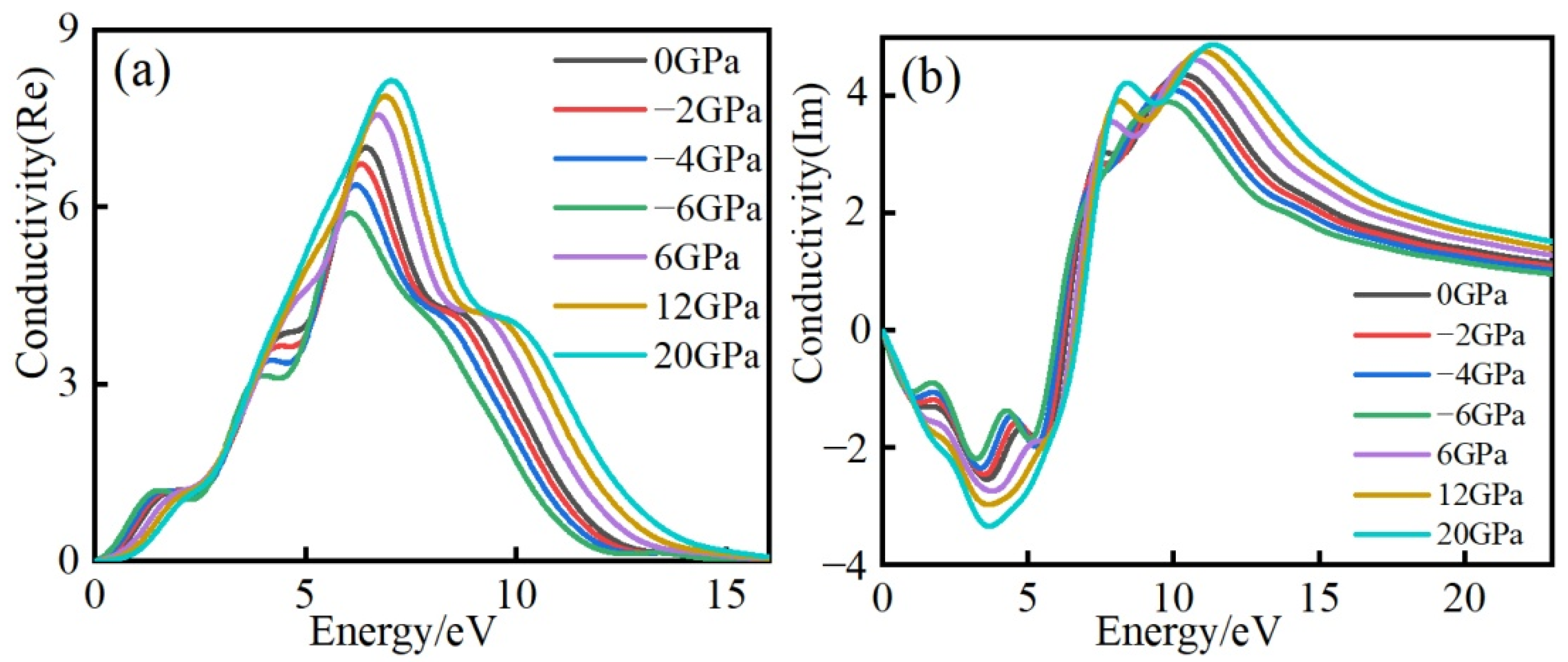
3.3.4. Complex Conductivity

It can be seen from Figure 9a that when the energy is less than 0.5 eV and greater than 12.6 eV, the real part of the complex conductivity is around 0—that is, there is almost no dissipation. It can be seen from the figure that the peak of the real part of the conductivity appears in the energy range of 1.5~8.8 eV, and the peak of the imaginary part appears in the energy range of 1.5~11.35 eV, which corresponds to the absorption spectrum. The real part of the conductivity reaches the maximum value near 6.4 eV. Combined with the analysis of the density of states map, it can be seen that these interband transition sources are related to the transition of Cu 3d orbital electrons to Sn 5p orbital electrons. With the increase intensile stress, the peak value of the real part of conductivity shifts to the direction of low energy, and with the increase incompressive stress, the peak value of the real part of conductivity shifts to the direction of high energy.

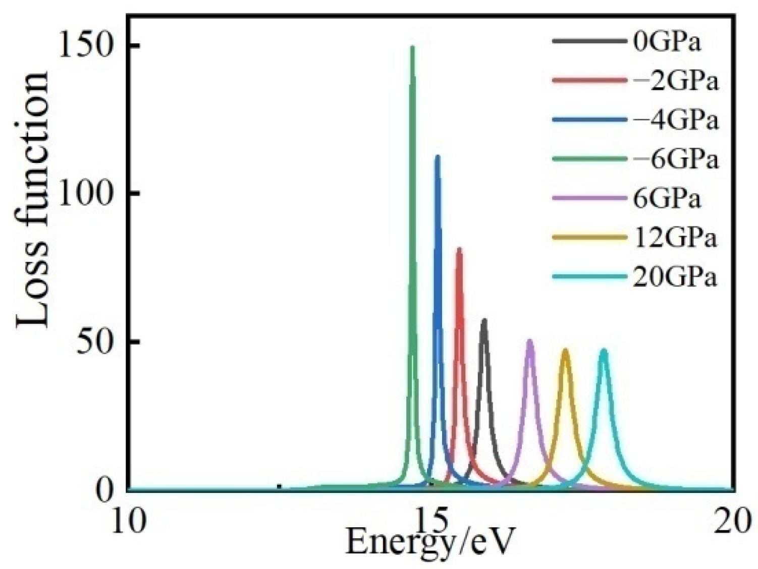
3.3.5. The Energy Loss Function

The energy loss function describes the energy loss of electrons when passing through a homogeneous medium. It can be seen from Figure 10 that the energy loss of Cu2ZnSnS4 reaches a maximum value of 57.22 near 15.89 eV at 0 GPa. When the stress is −6 GPa, the maximum energy loss is 149.23, and the minimum energy loss is 47.37 when the stress is 20 GPa.
With the increase intensile stress, the peak position of the energy loss function shifts to the lower-energy direction, and the peak value increases significantly with the increase intensile stress. With the increase incompressive stress, the peak position of the energy loss function shifts to the high-energy direction, and the peak value decreases slowly with the increase incompressive stress. This is mainly because the CZTS band gap changes significantly when the lattice is stretched, while the CZTS band gap changes slowly when the lattice is compressed. Therefore, applying stress can tune the peak position and peak value of the CZTS energy loss function.

4. Conclusions

By using the pseudopotential plane-wave method of first principles based on density functional theory, the band structure, density of states, and optical properties of Cu2ZnSnS4 under isotropic stress are calculated and analyzed. The CZTS band gap is reduced by stretching the lattice under isotropic stress, and increased by compressing the lattice. The band gap is 0.16 eV when no stress is applied. When the material is stressed, the atomic spacing becomes larger or smaller, which changes the Coulomb force. These changes lead to anincrease or decrease inexciton binding energy, which ultimately affects the electron transport and makes the band gap wider or narrower. The valence band of CZTS is mainly contributed by the 3d electrons of Cu, and the conduction band is mainly contributed by the 5s electrons of Sn. When the stress changes from −6 GPa to 20 GPa, CZTS always presents a direct band gap semiconductor at the high-symmetry point and maintains a tetragonal crystal system. At −6 GPa, the maximum static dielectric constant is 18.88, and the dielectric peak shifts to the high-energy direction with the increase instress. The absorption coefficient of CZTS in the visible light band is greater than 104 cm−1, and the reflectivity is lower than 30% in the energy range of 0.5~4.8 eV, showing good light absorption characteristics and low reflectivity. With the increase incompressive stress, the absorption peak of CZTS shifts towards the direction of high energy, and the peak value gradually increases. When the energy is greater than 16 eV, the refractive index is essentially constant, and the extinction coefficient is approximately 0. The maximum value of energy loss function is 57.22 near 15.89 eV, and the peak position of the energy loss function shifts to the direction of high energy with the increase incompressive stress, while the peak value decreases slowly with the increase incompressive stress. In summary, the band gap, optical absorption, dielectric constant, and other properties of CZTS can be adjusted by applying stress; this work provides a strong reference for the experimental preparation of high-quality CZTS films and can help in the development of efficient CZTS solar cells.

Author Contributions

Contributions, X.Y.; experimental design, X.Y.; simulation calculation, X.Y.; writing—review and editing, X.Q.; model building, X.Q.; data analysis, W.Y.; overall planning, W.Y.; review and revision of the thesis, C.Z.; drawing, C.Z.; literature review, D.Z.; software, D.Z.; analysis, B.G.; design of the question, B.G. All authors have read and agreed to the published version of the manuscript.

Funding

This research was funded by the Key Laboratory of Materials Simulation and Computing of Anshun University (Asxyxkpt201803), and the Youth Growth Project of Guizhou Provincial Department of Education, grant number KY (2020) 134.

Institutional Review Board Statement

Not applicable.

Informed Consent Statement

Not applicable.

Data Availability Statement

Not applicable.

Acknowledgments

The Youth Science and Technology Talent Growth Project of the Education Department of Guizhou Province (No.2020138), the Key Supporting Discipline of Materials and Aviation of Anshun College (2020), and the Guizhou Province JMRH Integrated Key Platform Funding Project.

Conflicts of Interest

The authors declare no conflict of interest.

References

  1. Yue, Q.; Liu, W.; Zhu, X. N-Type Molecular Photovoltaic Materials: Design Strategies and Device Applications. J. Am. Chem. Soc. 2020, 142, 11613–11628. [Google Scholar] [CrossRef] [PubMed]
  2. Sun, J.M.; Zhao, E.; Liang, J.; Li, H.; Zhao, S.; Wang, G.; Gu, X.; Tang, B.Z. Diradical-Featured Organic Small-Molecule Photothermal Material with High-Spin State in Dimers for Ultra-Broadband Solar Energy Harvesting. Adv. Mater. 2022, 34, 2108048. [Google Scholar] [CrossRef] [PubMed]
  3. Harijan, D.; Gupta, S.; Ben, S.K.; Srivastava, A.; Singh, J.; Chandra, V. High photocatalytic efficiency of α-Fe2O3-ZnO composite using solar energy for methylene blue degradation. Phys. B Condens. Matter 2022, 627, 413567. [Google Scholar] [CrossRef]
  4. Hu, Y.-H.; Li, M.-J.; Zhou, Y.-P.; Xi, H.; Hung, T.-C. Multi-physics investigation of a GaAs solar cell based PV-TE hybrid system with a nanostructured front surface. Sol. Energy 2021, 224, 102–111. [Google Scholar] [CrossRef]
  5. Celline, A.C.; Subagja, A.Y.; Suryaningsih, S.; Aprilia, A.; Safriani, L. Synthesis of TiO2-rGO Nanocomposite and its Application as Photoanode of Dye-Sensitized Solar Cell (DSSC). Mater. Sci. Forum 2021, 1028, 151–156. [Google Scholar] [CrossRef]
  6. Guo, W.H.; Zhu, Y.H.; Zhang, M.; Du, J.; Cen, Y.; Liu, S.; He, Y.; Zhong, H.; Wang, X.; Shi, J. The Dion–Jacobson perovskite CsSbCl4: A promising Pb-free solar-cell absorber with optimal bandgap 1.4 eV, strong optical absorption 105 cm−1, and large power-conversion efficiency above 20%. J. Mater. Chem. A 2021, 9, 16436–16446. [Google Scholar] [CrossRef]
  7. Das, B.; Hossain, S.M.; Nandi, A.; Samanta, D.; Pramanick, A.K.; Chapa, S.O.M.; Ray, M. Spectral conversion by silicon nanocrystal dispersed gel glass: Efficiency enhancement of silicon solar cell. J. Phys. D Appl. Phys. 2021, 55, 025106. [Google Scholar] [CrossRef]
  8. Yan, F.R.; Yang, P.Z.; Li, J.B.; Guo, Q.; Zhang, Q.; Zhang, J.; Duan, Y.; Duan, J.; Tang, Q. Healing soft interface for stable and high-efficiency all-inorganic CsPbIBr2 perovskite solar cells enabled by S-benzylisothiourea hydrochloride. Chem. Eng. J. 2021, 430, 132781. [Google Scholar] [CrossRef]
  9. Bi, P.; Zhang, S.; Chen, Z.; Xu, Y.; Cui, Y.; Zhang, T.; Ren, J.; Qin, J.; Hong, L.; Hao, X.; et al. Reduced non-radiative charge recombination enables organic photovoltaic cell approaching 19% efficiency. Joule 2021, 5, 2408–2419. [Google Scholar] [CrossRef]
  10. Khataee, A.; Azevedo, J.; Dias, P.; Ivanou, D.; Dražević, E.; Bentien, A.; Mendes, A. Integrated design of hematite and dye-sensitized solar cell for unbiased solar charging of an organic-inorganic redox flow battery. Nano Energy 2019, 62, 832–843. [Google Scholar] [CrossRef]
  11. Shen, L.; Li, H.; Meng, X.; Li, F. Transfer printing of fully formed microscale InGaP/GaAs/InGaNAsSb cell on Ge cell in mechanically-stacked quadruple-junction architecture. Sol. Energy 2020, 195, 6–13. [Google Scholar] [CrossRef]
  12. Lin, S.; Xie, S.; Lei, Y.; Gan, T.; Wu, L.; Zhang, J.; Yang, Y. Betavoltaic battery prepared by using polycrystalline CdTe as absorption layer. Opt. Mater. 2022, 127, 112265. [Google Scholar]
  13. Yeojun, Y.; Sunghyun, M.; Sangin, K.; Jaejin, L. Flexible fabric-based GaAs thin-film solar cell for wearable energy harvesting applications. Sol. Energy Mater. Sol. Cells 2022, 246, 111930. [Google Scholar]
  14. Fatemeh, G.Y.; Ali, F. Performance enhancement of CIGS solar cells using ITO as buffer layer. Micro Nanostruct. 2022, 168, 207289. [Google Scholar]
  15. Minemoto, T.; Matsui, T.; Takakura, H.; Hamakawa, Y.; Negami, T.; Hashimoto, Y.; Uenoyama, T.; Kitagawa, M. Theoretical analysis of the effect of conduction band offset of window/CIS layers on performance of CIS solar cells using device simulation. Sol. Energy Mater. Sol. Cells 2001, 67, 83–88. [Google Scholar]
  16. Pan, B.; Wei, M.; Liu, W.; Jiang, G.; Zhu, C. Fabrication of Cu2ZnSnS4 absorber layers with adjustable Zn/Sn and Cu/Zn+Sn ratios. J. Mater. Sci. Mater. Electron. 2014, 25, 3344–3352. [Google Scholar] [CrossRef]
  17. Tablero, C. Effect of the oxygen isoelectronic substitution in Cu2ZnSnS4 and its photovoltaic application. Thin Solid Films 2012, 520, 5011–5013. [Google Scholar] [CrossRef] [Green Version]
  18. Su, Z.H.; Liang, G.X.; Fan, P.; Luo, J.; Zheng, Z.; Xie, Z.; Wang, W.; Chen, S.; Hu, J.; Wei, Y.; et al. Device Postannealing Enabling over 12% Efficient Solution-Processed Cu2ZnSnS4 Solar Cells with Cd2+ Substitution. Adv. Mater. 2020, 32, 2000121. [Google Scholar] [CrossRef]
  19. Andrea, C.; Ole, H. What is the band alignment of Cu2ZnSn(S,Se)4 solar cells. Sol. Energy Mater. Sol. Cells 2017, 169, 177–194. [Google Scholar]
  20. Bao, W.; Ichimura, M. Prediction of the Band Offsets at the CdS/Cu₂ZnSnS₄ Interface Based on the First-Principles Calculation. Jpn. J. Appl. Phys. 2012, 51, 10NC31. [Google Scholar] [CrossRef]
  21. Su, Z.; Tan, J.; Li, X.; Zeng, X.; Batabyal, S.K.; Wong, L.H. Cation Substitution of Solution-Processed Cu2ZnSnS4 Thin Film Solar Cell with over 9% Efficiency. Adv. Energy Mater. 2015, 5, 1500682. [Google Scholar] [CrossRef]
  22. Kim, S.; Kim, K.M.; Tampo, H.; Shibata, H.; Niki, S. Improvement of voltage deficit of Ge-incorporated kesterite solar cell with 12.3% conversion efficiency. Appl. Phys. Express 2016, 9, 102301. [Google Scholar] [CrossRef]
  23. Chen, S.; Gong, X.G.; Wei, S.H. Band-structure anomalies of the chalcopyrite semiconductors CuGaX2 versus AgGaX2 (X=S and Se) and their alloys. Phys. Rev. B 2007, 75, 205209. [Google Scholar] [CrossRef] [Green Version]
  24. Walsh, A.; Chen, S.; Wei, S.H.; Gong, X.G. Kesterite Thin-Film Solar Cells: Advances in Materials Modelling of Cu2ZnSnS4. Adv. Energy Mater. 2012, 2, 400–409. [Google Scholar] [CrossRef]
  25. Tian, Y.; Zheng, Q.; Zhao, J. Tensile Strain-Controlled Photogenerated Carrier Dynamics at the van der Waals Heterostructure Interface. J. Phys. Chem. Lett. 2020, 11, 586–590. [Google Scholar] [CrossRef] [PubMed]
  26. Fan, L.L.; Chen, S.; Luo, Z.L.; Liu, Q.H.; Wu, Y.F.; Song, L.; Ji, D.X.; Wang, P.; Chu, W.S.; Gao, C.; et al. Strain Dynamics of Ultrathin VO2 Film Grown on TiO2 (001) and the Associated Phase Transition Modulation. Nano Lett. 2014, 14, 4036–4043. [Google Scholar] [CrossRef]
  27. LYU, L.; Yang, Y.Y.; CEN, W.F.; YAO, B.; OU, J.K. First-principles Study on Optical Properties of Cubic Ca2Ge under Stress Effect. Bull. Chin. Ceram. Soc. 2019, 38, 3788–3795. [Google Scholar]
  28. Yan, W.J.; Zhang, C.H.; Gui, F.; Zhang, Z. Electronic Structure and Optical Properties of Stressed β-FeSi2. Acta Opt. Sin. 2013, 33, 243–249. [Google Scholar]
  29. Lazarovits, B.; Kim, K.; Haule, K.; Kotliar, G. Effects of strain on the electronic structure of VO2. Phys. Rev. B 2010, 81, 115117. [Google Scholar] [CrossRef] [Green Version]
  30. Manyk, T.; Rutkowski, J.; Kopytko, M.; Martyniuk, P. Theoretical Study of the Effect of Stresses on Effective Masses in the InAs/InAsSb Type-II Superlattice. Eng. Proc. 2022, 21, 16. [Google Scholar]
  31. Schorr, S.; Hoebler, H.J.; Tovar, M. A neutron diffraction study of the stannite-kesterite solid solution series. Eur. J. Mineral. 2007, 19, 65–73. [Google Scholar]
  32. Segall, M.D.; Lindan, P.; Probert, M.J.; Pickard, C.J.; Hasnip, P.J.; Clark, S.J.; Payne, M.C. First-principles simulation: Ideas, illustrations and the CASTEP code. J. Phys. Condens. Matter 2002, 14, 2717–2744. [Google Scholar] [CrossRef]
  33. Perdew, J.P.; Burke, K.; Ernzerhof, M. Generalized Gradient Approximation Made Simple. Phys. Rev. Lett. 1996, 77, 3865–3868. [Google Scholar] [CrossRef] [PubMed] [Green Version]
  34. Vanderbilt, D. Soft self-consistent pseudopotentials in a generalized eigenvalue formalism. Phys. Rev. B 1990, 41, 7892–7895. [Google Scholar] [CrossRef] [PubMed]
  35. Liu, J. First-Principles Prediction of Structural, Elastic, Mechanical, and Electronic Properties of Cu2ZnSnS4 under Pressure. ECS J. Solid State Sci. Technol. 2022, 11, 073011. [Google Scholar] [CrossRef]
  36. Kumar, M.; Zhao, H.; Persson, C. Cation vacancies in the alloy compounds of Cu2ZnSn(S1−xSex)4 and CuIn(S1−xSex)2. Thin Solid Films 2013, 535, 318–321. [Google Scholar] [CrossRef]
  37. Kheraj, V.; Patel, K.K.; Patel, S.J.; Shah, D.V. Synthesis and characterisation of Copper Zinc Tin Sulphide (CZTS) compound for absorber material in solar-cells. J. Cryst. Growth 2013, 362, 174–177. [Google Scholar]
  38. Zhao, H.; Persson, C. Optical properties of Cu(In,Ga)Se2and Cu2ZnSn(S,Se)4. Thin Solid Films 2011, 519, 7508–7512. [Google Scholar] [CrossRef]
  39. Hoo, Q.Y.; Xu, Y. Detection of dielectric screening effect by excitons in two-dimensional semiconductors and its application. Acta Phys. Sin. 2022, 71, 124–138. [Google Scholar]
  40. Prokopidis, K.; Kalialakis, C. Physical interpretation of a modified Lorentz dielectric function for metals based on the Lorentz–Dirac force. Appl. Phys. B 2014, 117, 25–32. [Google Scholar] [CrossRef]
  41. Nainaa, F.Z.; Bekkioui, N.; Abbassi, A.; Ez, Z.H. First principle study of structural, electronic optical and electric properties of Ag2MnSnS4. Comput. Condens. Matter 2019, 22, e00443. [Google Scholar] [CrossRef]
  42. Scragg, J.J.; Dale, P.J.; Peter, L.M.; Zoppi, G.; Forbes, I. New routes to sustainable photovoltaics: Evaluation of Cu2ZnSnS4 as an alternative absorber material. Phys. Status Solidi 2010, 245, 1772–1778. [Google Scholar] [CrossRef]
  43. Kahlaoui, S.; Belhorma, B.; Labrim, H.; Boujnah, M.; Regragui, M. Strain effects on the electronic, optical and electrical properties of Cu2ZnSnS4: DFT study. Heliyon 2020, 6, e03713. [Google Scholar] [CrossRef] [PubMed]
Figure 1. Cu2ZnSnS4 unit cell structure.
Crystals 12 01454 g001
Figure 2. Band structure of Cu2ZnSnS4 under tensile stress for (a) 0 GPa band structure; (b) −2 GPa band structure; (c) −4 GPa band structure; (d) −6 GPa band structure.
Crystals 12 01454 g002
Figure 3. Band structure of Cu2ZnSnS4 under compressive stress for (a) 0 GPa band structure; (b) 6 GPa band structure; (c) 12 GPa band structure; and (d) 20 GPa band structure.
Crystals 12 01454 g003
Figure 4. Cu2ZnSnS4 density of states under tensile stress for (a) 0 GPa density of states and fractional density of states; (b) −2 GPa density of states and fractional density of states; (c) −4 GPa density of states and fractional density of states; (d) −6 GPa density of states and partial wave density of states.
Crystals 12 01454 g004
Figure 5. Cu2ZnSnS4 density of states under compressive stressfor (a) 0 GPa density of states and fractional density of states; (b) 6 GPa density of states and fractional density of states; (c) 12 GPa density of states and fractional density of states; (d) 20 GPa density of states and partial wave density of states.
Crystals 12 01454 g005aCrystals 12 01454 g005b
Figure 6. The complex dielectric function ofCu2ZnSnS4 under stress for (a) the real part of the complex dielectric function; (b) the imaginary part of the complex dielectric function.
Crystals 12 01454 g006
Figure 7. Absorption and reflection spectra for (a) the absorption spectrum and (b) the reflection spectrum.
Crystals 12 01454 g007
Figure 8. Complex refractive index for (a) the refractive index and (b) the extinction coefficient.
Crystals 12 01454 g008
Figure 9. Complex conductivity for (a) real part and (b) imaginary part.
Crystals 12 01454 g009
Figure 10. The energy loss function.
Crystals 12 01454 g010
Table 1. Cu2ZnSnS4 lattice constants of applied tensile and compressive stresses.
Stress/GPaa/b/c/V/Å3
−65.6885.68811.377368.043
−45.6025.60211.202351.220
−25.5285.52811.061338.034
05.4695.46910.944327.377
Theoretical [36]5.4695.46910.921326.647
Experimental [37]5.4275.42710.854319.676
65.3385.33810.673304.123
125.2405.24010.480287.732
205.1495.14910.242271.568
Publisher’s Note: MDPI stays neutral with regard to jurisdictional claims in published maps and institutional affiliations.

