3.1. Co-Design of Rectifier and Loop Antenna for High-Sensitivity Demodulation Systems
To meet the stringent requirements for high-sensitivity signal demodulation in low-power wake-up receivers, this section presents a co-design methodology for a rectifier and a loop antenna. This approach breaks from the conventional 50 Ohm matching network constraint by achieving direct conjugate impedance matching between the antenna and the multi-stage rectifier, with the goal of maximizing the energy transfer efficiency in the RF front-end [
15].
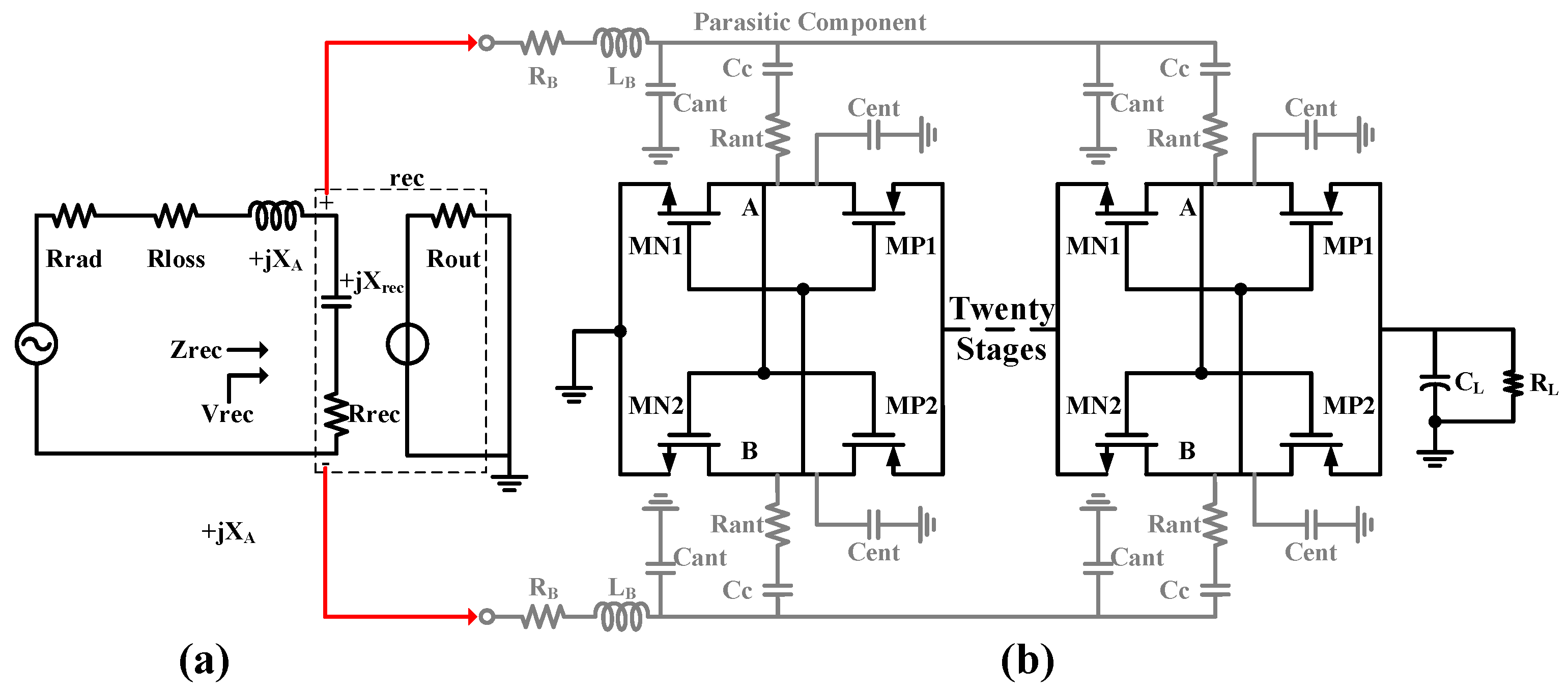
Figure 4a illustrates the equivalent circuit model of the proposed co-design. In this model, the antenna is characterized as a Thevenin equivalent circuit comprising a radiation resistance (
), a loss resistance (
), and an inductive reactance (
). The input impedance of the rectifier exhibits a capacitive characteristic (
). The quality factor (Q) of the rectifier is calculated as follows:
The equivalent parallel resistance and reactance are given by
The available output power at the antenna port is
High-sensitivity design aims to minimize the available power delivered by the antenna port for a given output voltage amplitude. From the above equations, it follows that higher sensitivity requires a higher quality factor (Q) of the rectifier and, simultaneously, a smaller real part of the impedance. The passive gain of the antenna is expressed as
where Va is the amplitude of the antenna equivalent voltage source and Vrect is the output voltage at the antenna port. Hence, the passive gain of the antenna rectifier LC resonant tank is Q/2, which further demonstrates that a high sensitivity rectification system necessitates a high Q design. However, a higher Q is not always preferable, as it increases the difficulty of antenna design and impedance matching. In this work, the design value of Q is chosen to be in the range of 30 to 50.
The rectifier employs a differentially driven cross-coupled topology. The advantage of this structure is that the cross-coupled connection dynamically compensates for the MOSFET threshold voltage, thereby reducing the effective turn-on voltage of the transistors. Simultaneously, transistors with a medium threshold voltage, approximately 300 mV, are used. Under conditions of low input power, the voltage induced at the antenna port is too low, forcing the transistors to operate in the deep sub-threshold region. A multi-stage cascaded configuration is therefore essential to boost the output voltage. To minimize parasitic capacitance, the transistor channel length L is set to its minimum value. In the design iteration, the number of stages primarily depends on the antenna port voltage and the target output voltage. The output voltage itself is determined by the design threshold of the subsequent circuitry. In this work, to enhance system robustness, the output voltage must not fall below 20 mV. The determination of the other two key design variables—the number of stages and the transistor width W—embodies the core concept of the antenna-rectifier co-design. The iterative design flow is as follows:
Step 1: Given a rectifier input port voltage (e.g., 10 mV), initial values are set for the number of stages and W. The output voltage, impedance, and Q-factor are then simulated.
Step 2: Based on the results from Step 1, a matching antenna is designed. Its gain, efficiency, and size are obtained, and the system sensitivity is evaluated.
Step 3: The process loops back to Step 1. The number of stages and W are iteratively optimized, with corresponding antennas designed and system sensitivity calculated for each iteration.
Step 4: After multiple optimization iterations, the system sensitivity converges to an optimal range, indicating that the system performance has reached its best balance point.
Upon completion of the iterative design, the rectifier employs a 20-stage cascade. When the antenna port voltage is 10 mV, the output exceeds 20 mV. The final rectifier design achieves a Q-factor of 40. After impedance matching, the sensitivity is better than −50 dBm.
In the practical design process, the impact of the layout on performance is critical. Given that the rectifier’s input impedance is primarily constrained by its internal parasitic capacitances, and considering that pre-layout simulation results may deviate significantly from post-layout simulations incorporating parasitic parameters—while rectification sensitivity is directly dependent on the accuracy of the input impedance—a specific design flow was adopted. This flow involved first completing the layout of the cascaded rectifier, followed by parasitic parameter extraction for post-layout simulation. Finally, the extracted parasitic parameters were back-annotated to the schematic for re-simulation, thereby minimizing impedance deviation.
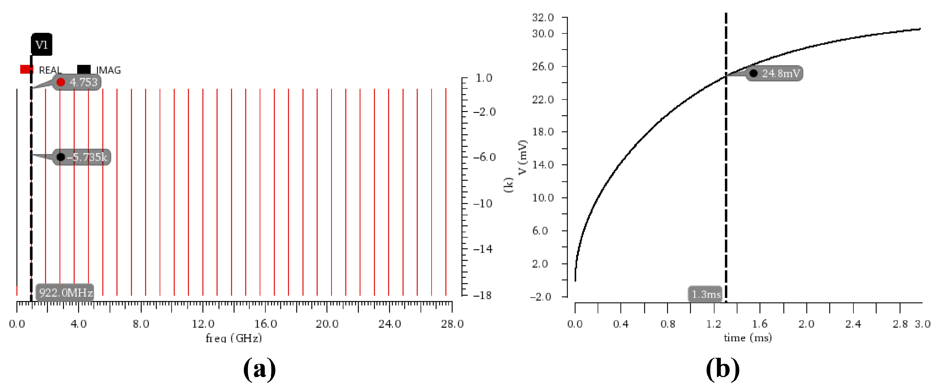
Simulation results (
Figure 5a) demonstrate that through precise optimization of the NMOS transistor width-to-length ratio (W/L), the rectifier achieves an input impedance of 4 − j×372 Ohm at the target operating frequency of 922.5 MHz. This provides a foundation for effective co-design with the antenna. Further simulations (
Figure 5b) verify that when the input signal amplitude is as low as 10 mV, the structure, leveraging its multi-stage voltage multiplication effect, can generate an output voltage exceeding 25 mV within 1.3 ms. This output is sufficient to reliably trigger subsequent circuitry into operation.
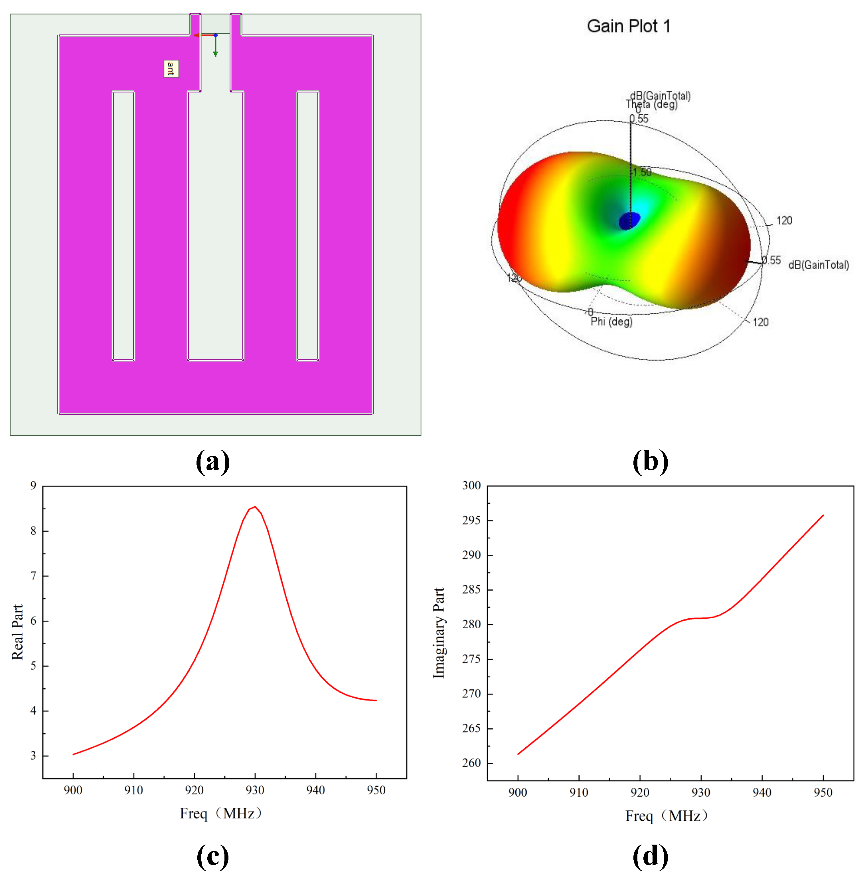
At 922.5 MHz, a dipole antenna would have a size approximating half the wavelength of the electromagnetic wave, exceeding 15 cm. This dimension is considered too large to meet the compact-device design requirements of the wake-up receiver. To achieve a balance between compact size and performance, this paper adopts a loop antenna topology. The design of the customized antenna is illustrated in
Figure 6. Accounting for post-layout simulation results of the chip and the parasitic capacitance introduced by the Chip-on-Board (COB) packaging, the antenna impedance is designed to be 5 + j×280 Ohm. The antenna measures 4.5 cm by 4.8 cm, with a gain of 0.76 dBi. This design prioritizes a compact form factor at the expense of higher gain, achieving a radiation efficiency of 82%. The radiation efficiency is calculated using the following formula:
The calculated Rloss resistance is approximately 0.8 Ohm. Due to the high Q-factor of the rectifier and the frequency-dependent variations in both the real and imaginary parts of the antenna impedance, the system exhibits a relatively narrow bandwidth. Simulation results indicate a 3-dB bandwidth of 20 to 25 MHz. Despite the sensitivity of antenna impedance to fabrication and environmental conditions, the loop antenna used in this design exhibits a gradual frequency-dependent impedance variation. This characteristic allows the high-Q resonant system to retain sufficient matching bandwidth under practical operating conditions.
Figure 6 depicts the key characteristics of the proposed antenna: (a) the antenna structure, (b) the simulated antenna gain, (c) the evolution of the real part of the antenna impedance versus frequency, and (d) the evolution of the imaginary part of the antenna impedance versus frequency.
3.2. Mean-Detection Demodulation Circuit Design for Shallow Modulation Applications
3.2.1. Signal Amplifier
To meet the performance requirement of high-sensitivity reception in long-range communication scenarios, this paper designs a dedicated signal amplification circuit for the RF analog front-end. When receiving weak RF signals, even after the voltage multiplication effect of the rectifier, the amplitude of its output signal typically remains at the millivolt level, which is insufficient to effectively drive the subsequent decision circuit. Therefore, introducing a signal amplification stage with substantial gain is crucial. This stage must amplify the DC signal from the rectifier output to a level suitable for reliable decision-making by the subsequent comparator.
In an architecture that employs passive gain and prioritizes envelope detection, and where no RF amplification stage is placed at the very front-end of the signal path, the overall sensitivity of the system largely depends on the noise introduced by the envelope detector and the subsequent amplification circuit. Consequently, careful noise optimization of the amplifier circuit becomes a key design consideration for achieving high sensitivity [
16]. Simultaneously, given the system’s stringent requirement for ultra-low power consumption, the amplifier circuit must achieve excellent noise performance within a limited power budget. Based on this, instead of adopting complex, high-power-consumption special circuit structures, this design opts for a standard low-power architecture followed by targeted optimization and design.
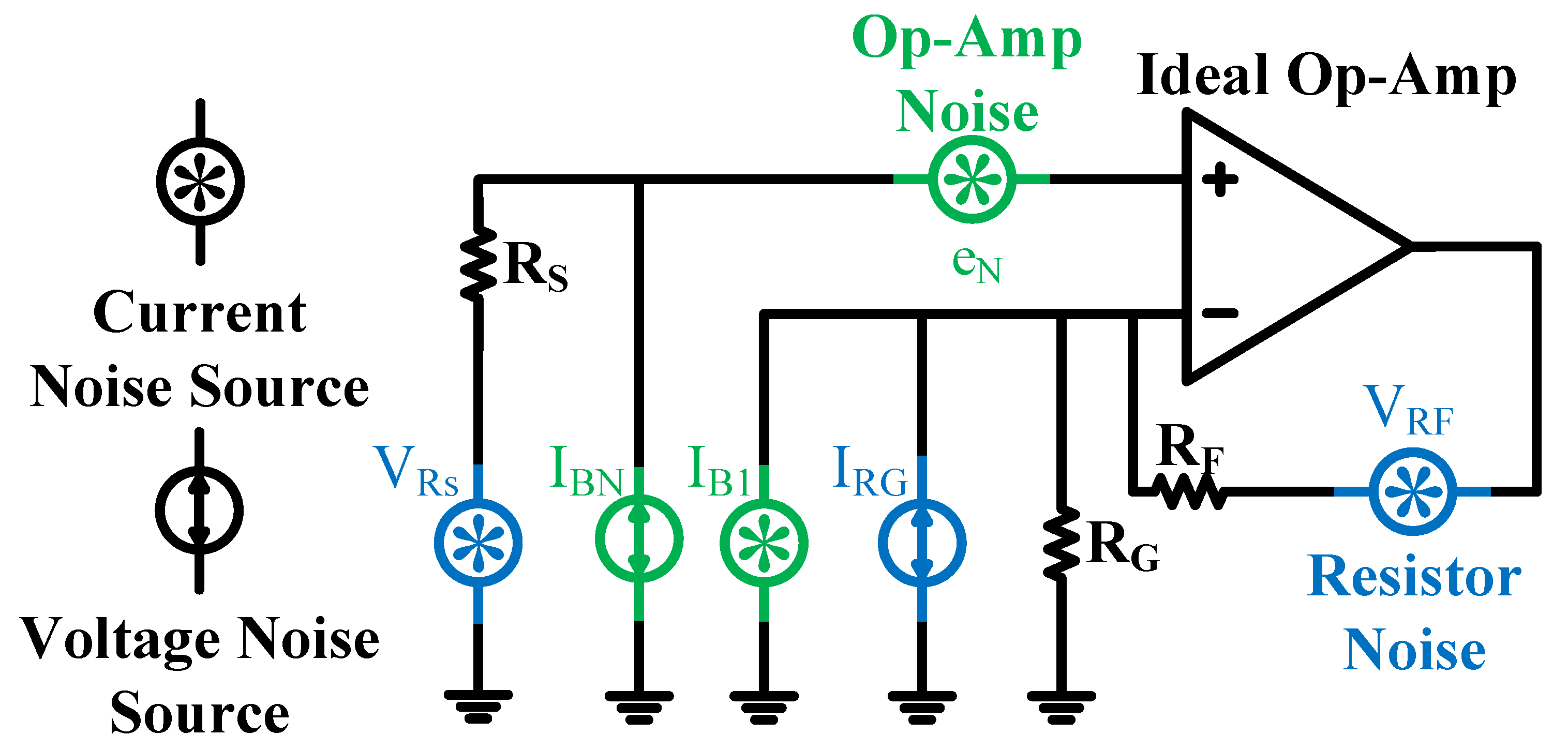
Figure 7 shows the equivalent circuit model of the non-inverting operational amplifier, including its noise sources. The total output noise of this circuit is primarily composed of the root mean square sum of individual noise components. Its theoretical expression is given by
Noise analysis was performed and verified using the Cadence simulation platform (version IC618). Owing to the narrow bandwidth of the amplifier, the equivalent input-referred noise voltage, calculated by integrating the internal noise over the frequency band of interest and referring it to the input, is approximately 41.2 µV. This noise level is within the acceptable design tolerance and meets the specified noise performance requirements for the front-end amplification circuit.
3.2.2. Mean-Detection Circuit
In conventional design schemes, the reference voltage for the decision comparator is typically generated by either a low-pass filter or a peak-detection circuit. When employing a low-pass filter, the essence of the approach lies in extracting the signal average using an RC filtering network with a large time constant. Although the filtering-based method offers good stability, in scenarios where the transmitted signal is a continuous wave, the voltage difference between the filtered output signal and the envelope signal can be minimal, which may easily lead to decision errors. If the peak-detection method is adopted—where the signal peak is detected and held, and half of this value is used as the reference level—this approach heavily relies on the signal’s modulation depth. It requires a deep modulation condition (typically demanding a modulation depth greater than 50%) to function effectively.
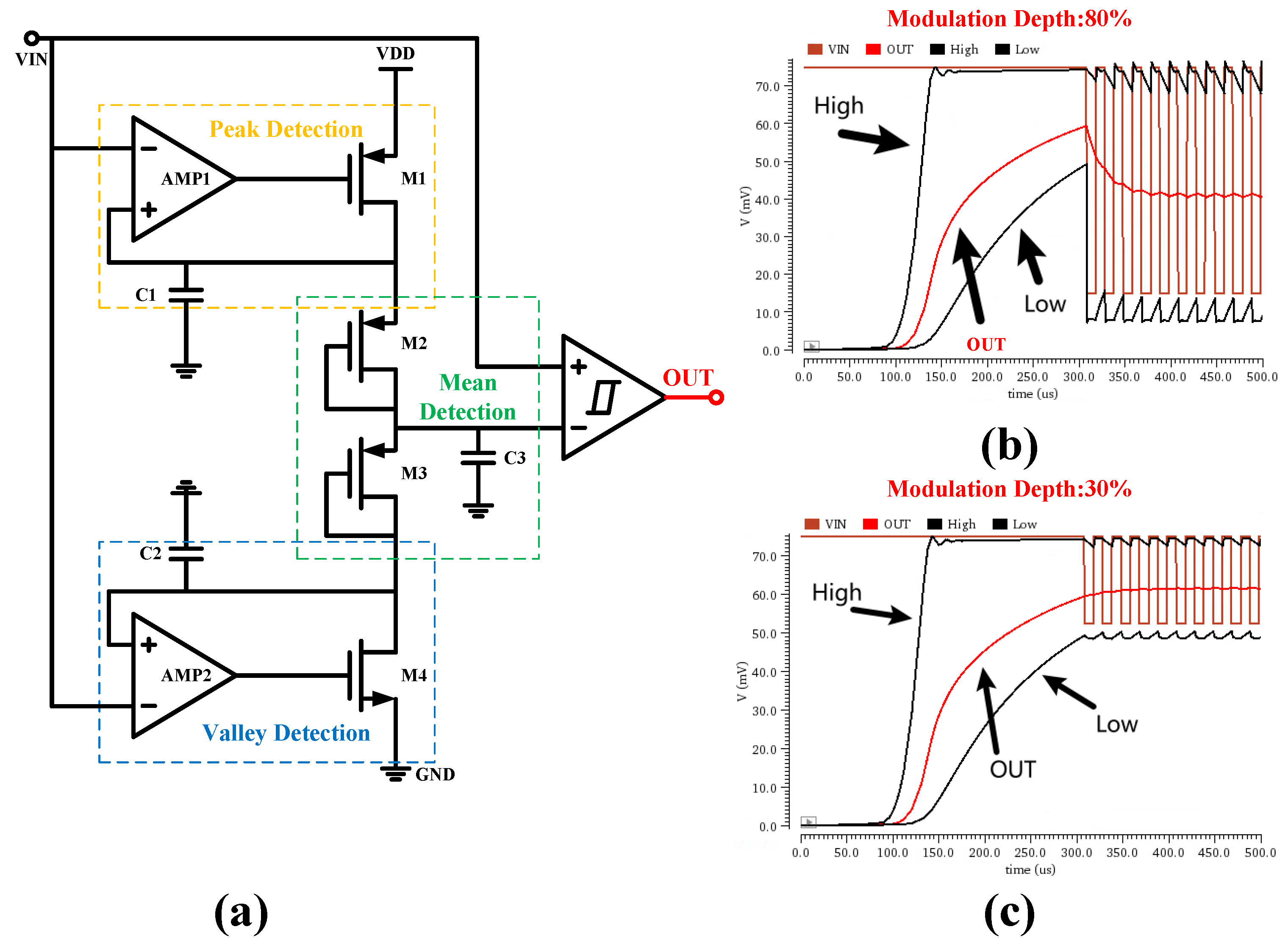
To address the technical challenges in demodulating shallowly modulated signals, this study proposes an innovative mean-detection circuit architecture, whose basic structure is shown in
Figure 8a. This circuit comprises three main parts: a peak detection unit, a valley detection unit, and a voltage divider network. Its core innovation lies in the ability to track the peak (V
max) and valley (V
min) values of the input signal in real-time and compute their average to serve as the reference level:
The peak detection unit (AMP1, MP3, MP4) is responsible for monitoring the input signal. It triggers the corresponding control logic when the input voltage falls below the voltage stored on capacitor C1. The valley detection unit (AMP2, AMP3, MP4), conversely, controls the capacitor discharge process, enabling the voltage to track the signal’s valley level. The voltage divider network (M2, M3, C3) performs level shifting on the processed signal, completing the entire signal conditioning flow. Through precise timing coordination among these units, fast and accurate detection of the input envelope signal is achieved.
To verify the performance of the proposed circuit, simulations were conducted under conditions of 27 °C ambient temperature and a 0.5 V supply voltage. The simulation was set with all devices at the tt process corner. The envelope signal input to the mean-detection circuit was pre-processed by the pre-amplifier, with its DC level set to 75 mV. Simulation results under modulation depths of 80% and 30% are shown in
Figure 8b and
Figure 8c, respectively. The results demonstrate that the circuit architecture maintains stable performance across different modulation depths, effectively overcoming the limitations of traditional demodulation circuits under shallow modulation conditions.
3.2.3. Dynamic Comparator Design
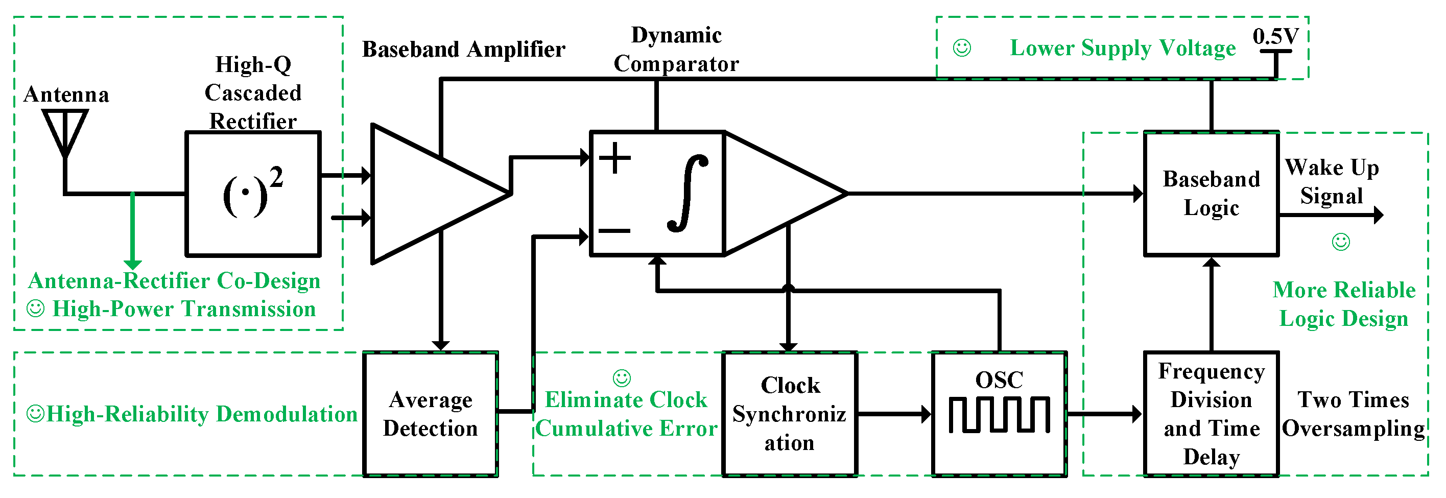
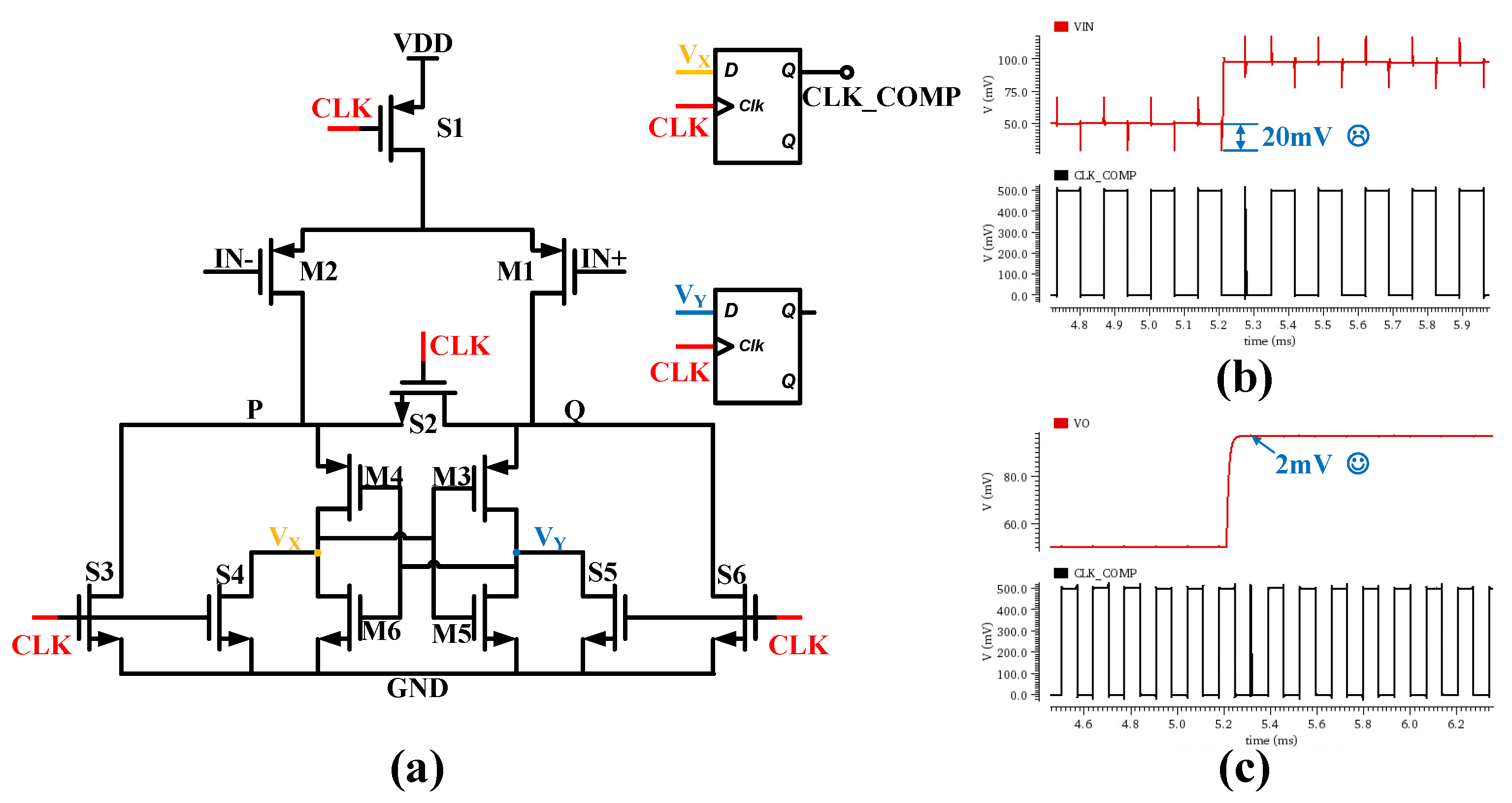
To achieve the design goals of low power consumption and high reliability, this study employs a dynamic comparator architecture based on the StrongArm latch topology (its circuit structure is shown in
Figure 9a [
17], replacing conventional hysteresis comparators that exhibit significant static power consumption. This dynamic comparator operates at a 4 kHz sampling frequency. Its core structure consists of an input differential pair (M1, M2) and a cross-coupled regenerative latch unit (M3–M6), with switching between reset and evaluation phases achieved through seven clock-controlled switches (S1–S6).
When the clock signal (CLK) is high, the circuit enters the reset phase, and its internal critical nodes are reset to ground (GND). When the clock signal transitions to low, the circuit enters the evaluation phase: the input pair transistors M1 and M2 turn on, allowing the supply voltage (VDD) to charge the nodal capacitors through them. An input voltage difference
causes a current imbalance between the left and right branches. This current difference is rapidly regenerated and amplified by the cross-coupled positive feedback latch structure formed by M3–M6, driving the node with the higher voltage quickly to the logic high level and the other node to the logic low level. The output signal is conditioned by a buffer stage and then precisely latched by a subsequent D-type flip-flop on the rising clock edge. To eliminate offset introduced by load mismatch, a symmetrical D-type flip-flop structure is also configured in the other differential signal path. One of the primary technical challenges in dynamic comparators is kickback noise. This noise originates from voltage spikes coupled into the preceding sensitive circuitry through parasitic parameters—such as gate-to-source capacitance (Cgs), body-to-source capacitance (Cbs), and gate-to-drain capacitance (Cgd)—of switching transistors (M1 and M2) when the clock signal transitions.To effectively suppress kickback noise, this study introduces a filtering capacitor at the input stage of the comparator. The circuit employs a 1 pF capacitor, whose value is significantly larger than the parasitic capacitances of the switching transistors. As shown in the VIN signal in
Figure 9b—which corresponds to the case without the filter capacitor at the comparator input—a noise glitch of approximately 20 mV caused by kickback noise is clearly observable. Such glitches can readily lead to comparison errors in subsequent cycles. In contrast, as illustrated in
Figure 9c, after adding the filter capacitor at the comparator input, the kickback noise on the VO signal is effectively suppressed. The resulting kickback voltage at the input manifests only as a minor pulse spike of about 2 mV, which does not cause erroneous decisions.
3.2.4. Performance Simulation and Verification
System-level simulations were conducted to validate the proposed demodulation circuit operating at a 0.5 V supply voltage. The circuit architecture integrates a fully differential rectifier, a signal amplification circuit, a mean-detection circuit, and a decision comparator.
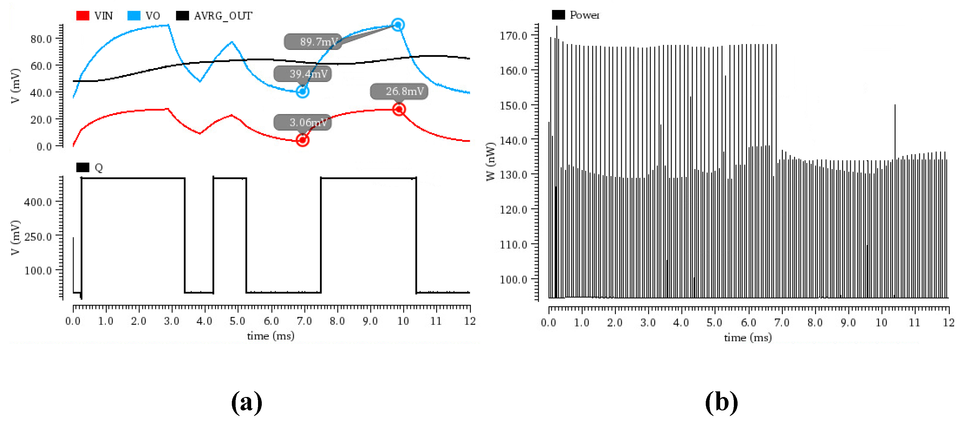
Under test conditions of a 25 mV input signal amplitude, a 2 kbps modulation rate, and an 80% modulation depth, the simulation results are shown in
Figure 10a. After processing by the amplification circuit, the peak value of the rectifier’s output signal was amplified to 89.7 mV, corresponding to a voltage gain of approximately 3 times. However, the valley value exhibited asymmetric amplification behavior, achieving a gain of 13 times, which consequently reduced the modulation depth from the initial 80% to 56.3%. This phenomenon indicates effective detection capability for weak signals, while also revealing linearity limitations of the amplification circuit under very small input signal conditions, highlighting the necessity for a high dynamic range design. Despite this nonlinear amplification, the demodulated output signal exhibited only a 2% timing error in pulse width, indicating well-maintained timing characteristics. Regarding power consumption, the simulation results, shown in
Figure 10b, indicate that the circuit consumes 94.61 nW during normal operation, achieving a good balance between low-power operation and functional integrity. These simulation results provide an important reference for subsequent circuit performance optimization and system-level design.
3.3. Correlator Logic Baseband and Clock Synchronization Circuit Design
To address the key challenges in baseband processing and clock management for low-power wake-up receivers, this chapter presents the design and implementation of a high-reliability, low-power correlator logic baseband and clock synchronization circuit. The design employs a wake-up code verification method based on Hamming distance, incorporates a configurable error tolerance threshold, and utilizes a data-edge-triggered synchronization mechanism. Operating stably at an ultra-low supply voltage of 0.5 V, the design effectively mitigates cumulative phase errors and sampling synchronization issues caused by clock drift during long data packet transmission.
3.3.1. Correlator Logic Baseband Design
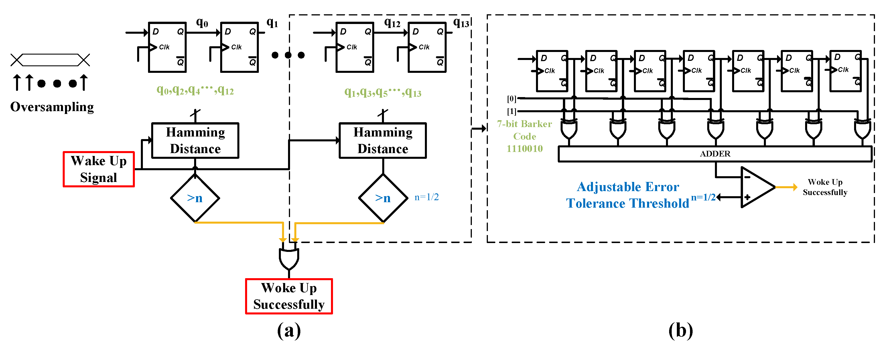
To meet the stringent ultra-low power requirement of the wake-up receiver, this design adopts a low data-rate encoding scheme, setting the data transmission rate of the analog front-end to 1 kbps. Given the characteristic of the dynamic comparator to maintain its previous sampling state until the arrival of the next sampling clock edge, the sampling frequency should theoretically be maximized to improve decision accuracy. In this scheme, the 8 kHz main clock signal is directly used as the reset clock for the dynamic comparator to achieve oversampling of the input signal. Concurrently, the main clock is frequency-divided and delayed to generate a 2 kHz clock, which serves as the sampling clock for the correlator logic, resulting in two sampling bits per input data bit, thereby effectively implementing oversampling. Research [
18,
19,
20] has demonstrated that oversampling techniques can effectively alleviate phase misalignment caused by clock frequency deviations and possess the potential to suppress noise and enhance the signal-to-noise ratio (SNR).Double oversampling is employed with a 4 kHz clock, thereby further enhancing system robustness. For other application scenarios, the sampling clock frequency needs to be selected according to the specific practical conditions.
The serial data output from the comparator is first converted into a parallel format by a shift register before being fed into the subsequent correlator for processing. The data has already been oversampled at the shift register stage, this design adopts a grouped correlator architecture. The primary distinction between this architecture and a conventional correlator lies in its incorporation of two independent operating phases. As illustrated in
Figure 11a, each phase consists of a seven-bit shift register with an identical structure, responsible for performing a bit-by-bit comparison between the input bit stream and a locally stored wake-up code. When the correlation value output from either phase exceeds a preset threshold, the system determines that a valid wake-up signal has been detected and generates the corresponding wake-up command.
Figure 11b shows the logic structure of the 7-bit correlator. The correlator logic typically comprises fundamental building blocks such as a shift register, an array of XOR gates, NOT gates, and a multi-bit adder.The shift register, implemented by cascading multiple D-flip-flops, functions to convert serial input data into parallel output. The core operation of the correlator is based on the calculation of the Hamming distance. Each bit of the shift register’s output and the corresponding bit of the preset wake-up code are connected to an XOR gate. When the corresponding bits match, the XOR gate outputs a ‘0’; when they mismatch, it outputs a ‘1’. The outputs of these XOR gates are inverted by NOT gates and then fed into a multi-bit adder for summation. The output of the adder reflects the degree of difference between the received data and the preset wake-up code—specifically, a smaller Hamming distance indicates a higher degree of match, resulting in a larger numerical value at the adder’s output. Finally, this output value is compared against a configurable threshold. If the value exceeds the set threshold, a wake-up signal is generated to activate the main receiver.
By appropriately setting the error tolerance threshold (this system supports 1-bit or 2-bit fault tolerance) [
21], a balance can be effectively struck between the probability of false wake-ups and missed wake-ups, thereby enhancing the system’s robustness in practical interference-prone environments. Considering the constraints of coding efficiency, fault tolerance capability, and power consumption collectively, this work selects the 7-bit Barker code (code sequence: 1011100) as the wake-up identifier. Combined with the two-phase oversampling correlator design, this approach significantly improves tolerance to clock frequency deviations, providing a highly reliable wake-up decision solution for low-power Internet of Things (IoT) communication.
3.3.2. Custom Low-Voltage Correlator Logic Using an Analog-Oriented Design Approach
To optimize the overall system power consumption, the supply voltage for this design is set to 0.5 V. However, standard digital cell libraries typically require a 1 V supply, making them unsuitable for direct application in such an ultra-low voltage scenario. This section, therefore, proposes a customized design flow for implementing the low-voltage digital logic and presents simulation results verifying the functionality and power characteristics of the designed circuit. A customized methodology, rooted in analog circuit design practices, is employed for this low-voltage digital logic.
The process begins with a behavioral-level description of the digital baseband module using Verilog HDL. The primary functions of this module include initializing the wake-up command output and resetting the shift register states when the reset signal is asserted, and sampling and shifting the input data on the rising edge of the clock signal to convert serial data into a parallel format. The parallel data bits (specifically bits 0, 2, 4, 6, 8, 10, 12 and bits 1, 3, 5, 7, 9, 11, 13) are grouped into two sets for separate summation operations. A valid wake-up signal is generated if the summation result from either set exceeds a preset fault-tolerant threshold. This threshold is dynamically configurable via an external level signal: a low level indicates the system tolerates a 1-bit error, while a high level indicates tolerance for a 2-bit error.
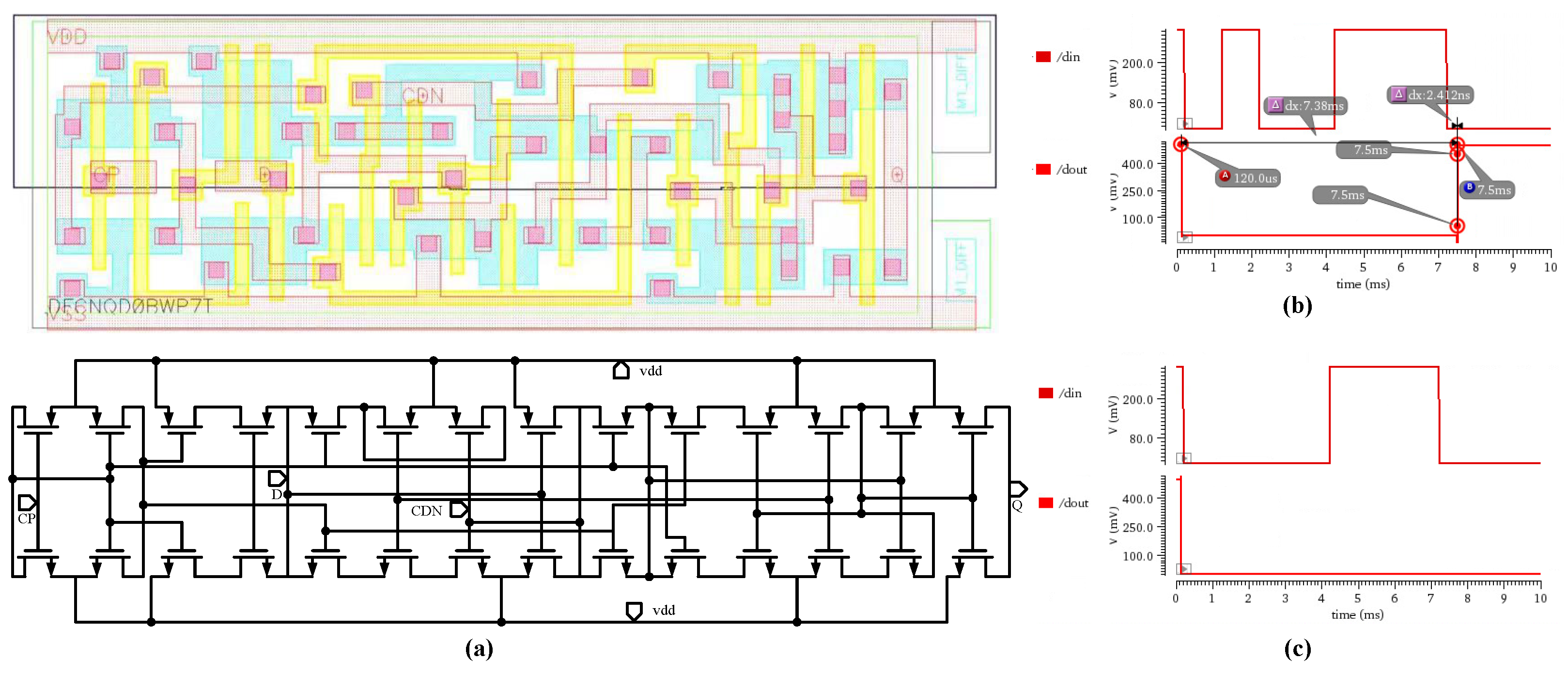
Following logic synthesis, the generated netlist is imported into the Cadence Virtuoso platform and converted into a circuit schematic. It is important to note that, due to the lack of ready-made low-voltage device schematics for 0.5 V operation in the standard cell library, the circuit structures of basic logic gates were reverse-extracted from the standard cell layouts and manually augmented with power and ground pins. For instance,
Figure 12a illustrates the layout structure and the subsequently extracted transistor-level schematic of a low-level reset, positive-edge-triggered D-type flip-flop (DFCNQD0BWP7T).
After finalizing the circuit schematics, a simulation analysis was conducted on the module. The simulation parameters were configured as follows:the operating clock frequency was 2 kHz, the input data rate was 1 kbps, the modulated signal used a 7-bit Barker code (sequence: 0100111) with a high level of 500 mV and a low level of 0 V, and the supply voltage was 0.5 V. The simulation results are shown in
Figure 12b. After the system completely received the 7-bit Barker code, it successfully generated a valid wake-up command signal. The output signal’s transition time was 2.4 ns, and the total delay from system reset to the generation of the wake-up command was approximately 7.5 ms, indicating that the wake-up decision was completed at the first rising clock edge after receiving the entire 7-bit code. In terms of power consumption, since the digital baseband module primarily incurs dynamic power consumption during clock transitions, its overall power consumption remains at an extremely low level. Simulation results show that the average power consumption for a complete process, from data reception to wake-up decision, is on the order of picowatts (pW). To evaluate the fault tolerance of the baseband module, a test was further conducted using a Barker code with a one-bit error in the input sequence (sequence: 0000111). As shown in
Figure 12c, when the error tolerance threshold was set to zero (i.e., no fault tolerance), the system did not trigger a wake-up command because the input data did not perfectly match the internally preset reference code. This result verifies that the designed baseband module possesses strict false wake-up suppression capability.
3.3.3. Clock Synchronization Circuit Design
In On-Off Keying (OOK) modulated wake-up receivers, the baseband logic must reliably decode the baseband bit stream demodulated by the analog front-end. Existing schemes often employ oversampling or digital control techniques to overcome phase misalignment between the data and the internal clock. When the data rate is fixed, frequency errors primarily stem from deviations of the internal clock source; consequently, a high-precision clock is crucial for system performance [
22]. However, conventional high-precision clock sources, such as phase-locked loops (PLLs) or crystal oscillators, are often unsuitable for semi-active, low-power scenarios due to their high power consumption and large area overhead.
The design of the sampling clock must fulfill two key requirements. First, the sampling point should be aligned near the center of the data bit to equally tolerate positive and negative frequency deviations. Second, the accumulation of phase error must be suppressed through a synchronization mechanism to enhance the reliability of long data packet reception, preventing error buildup during sequences of consecutive identical bits. To meet these requirements, this paper proposes a data-edge-triggered clock synchronization logic specifically designed for ultra-low-power and long-data transmission scenarios. Based on a gated oscillator clock and data recovery (GO-CDR) architecture [
23], this logic maintains phase and frequency synchronization between the data and the local sampling clock without relying on traditional PLLs.
The circuit structure, shown in
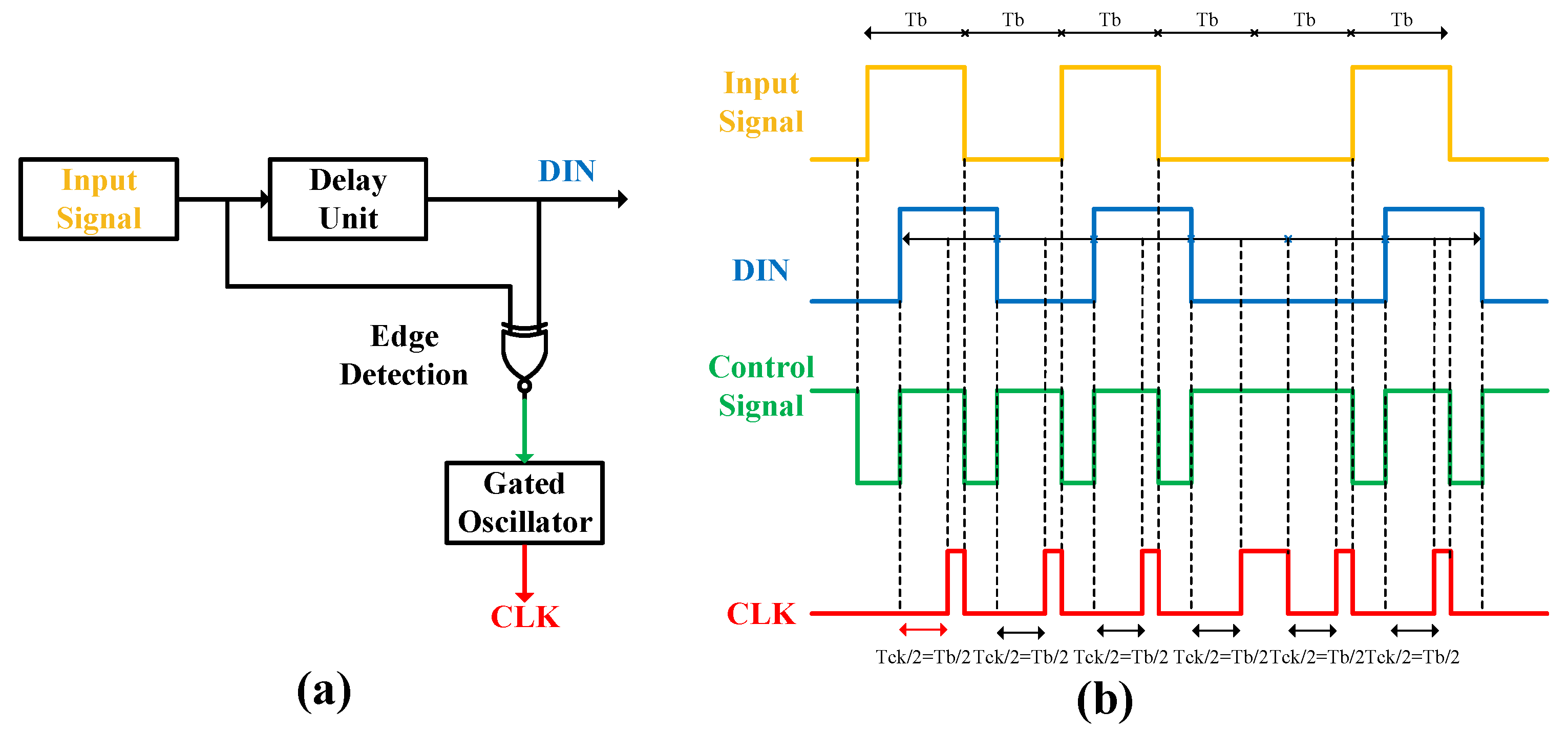
Figure 13a, primarily consists of three parts: a delay unit, an edge detection circuit based on an XNOR gate, and a gated oscillator. The input data signal is delayed by a unit to generate a DIN signal with a delay of
. The edge detector produces a reset pulse with a width of
whenever a transition occurs in the input data; its output remains high at other times. The gated oscillator operates as follows: when its control signal is high, the oscillator runs freely, generating a clock signal with frequency
= 1/
. When a low-level pulse appears on the control signal, the oscillator is reset to its initial state. Assuming the unit interval
equals the clock period
, its operational waveform is depicted in
Figure 13b.
Each transition in the input data triggers a low-level pulse from the edge detector, which resets the gated oscillator, thereby clearing any accumulated phase error. After the control signal returns high, the oscillator restarts its free-running operation. Ideally, the first rising clock edge occurs at /2, aligning the sampling edge to the center of the data bit and achieving synchronization between the data edge and the sampling clock. As long as the control signal remains high, the DIN signal is continuously sampled at the frequency . If a discrepancy exists between and , phase error accumulates during non-transition intervals; however, this error is cleared at the next data transition. Therefore, the limiting factor for long-packet reception is not the total data length but the maximum length of consecutive identical bits (CIB). The sampling circuit is designed to be immune to noisy data edges. In the synchronization logic, a multi-stage inverter delay chain is introduced during the clock synchronous reset to ensure that sampling occurs near the center of the data level. This delay chain is sufficient to cover all data edge noise, thereby guaranteeing that the circuit remains unaffected by noisy data edges when the sampling clock arrives.The circuit proposed in this work achieves a significant power reduction to the nanowatt level while meeting the target application requirements.
3.3.4. Design of the Gated Oscillator, Delay, and Edge Detection Module
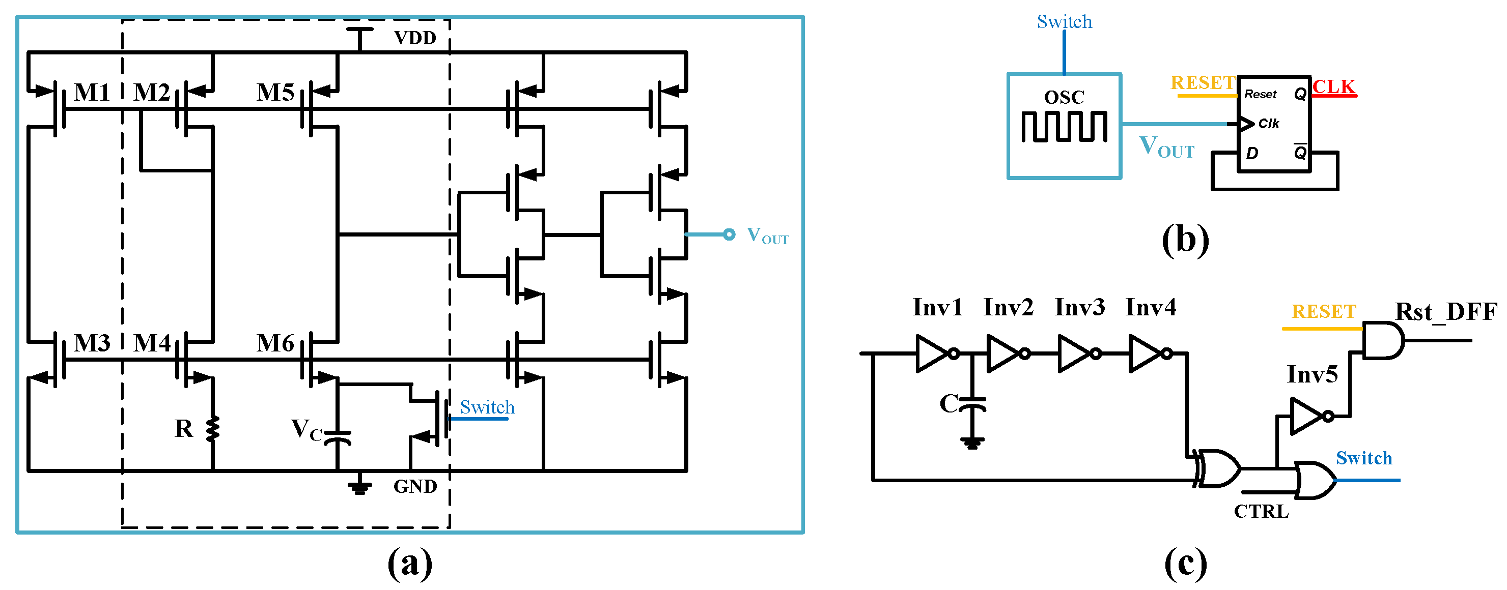
Figure 14a illustrates the gated oscillator circuit proposed in this work [
24], which serves as the primary clock source for the wake-up receiver, generating an 8 kHz square wave signal with a 50% duty cycle. This oscillator comprises a reference current generation circuit, an inverter chain, and a reset switch. The reference circuit, where transistors M2 and M4–M6 operate in the subthreshold region, generates a reference current, Iref. By utilizing an external 5.5 M Ohm high-value resistor, Iref is reduced to approximately 7.5 nA, enabling the oscillator to achieve nanowatt-level power consumption. The oscillator operates based on a capacitor charging-discharging mechanism: when the capacitor voltage exceeds a reference voltage, the comparator toggles, producing the clock output. A gating signal, generated by an edge detector, controls the reset switch to discharge the capacitor when necessary for phase synchronization. The output stage employs a current-starved inverter as a buffer to further optimize power consumption.
To enhance clock period stability, a frequency divider circuit based on a D-type flip-flop is incorporated after the oscillator, as shown in
Figure 14b.
The delay and edge detection module, depicted in
Figure 14c, introduces a controlled delay to the input signal using an inverter chain (Inv1–Inv4) and a nodal capacitor, C. The delayed signal and the original signal are fed into an XOR gate to generate the gating signal. According to the oscillator’s operational logic, the oscillator runs in a free-running state when the gating signal is low. Consequently, this gating signal is OR-combined with the oscillator output, Vout, and the result is used as the reset control signal for the internal charging capacitor of the oscillator. Simultaneously, the inverted gating signal is AND-ed with the global system reset signal, RESET, to generate the reset signal for the subsequent D-type flip-flop (this flip-flop is active low). The delayed signal from the output of the delay module ultimately serves as the baseband data input, which is transmitted to the digital baseband logic unit for subsequent processing.
3.3.5. Overall Simulation of the Clock Synchronization Module
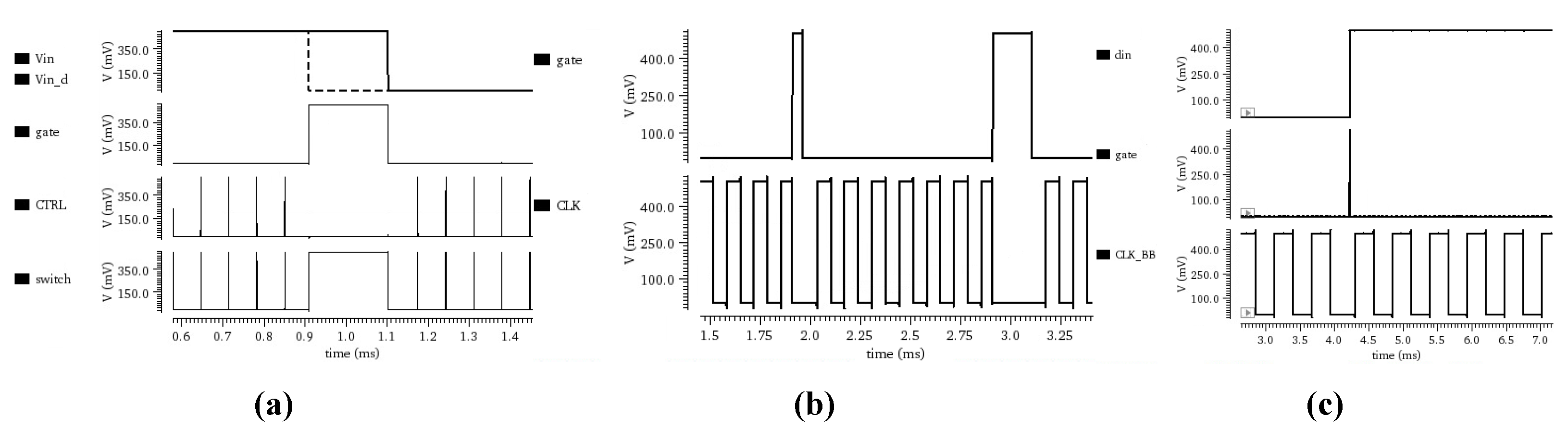
To verify the functional correctness and power characteristics of the proposed clock synchronization module, a transient simulation analysis was conducted. The simulation results are shown in
Figure 15 The waveform characteristics at key nodes and the corresponding operational mechanisms for each sub-module are elaborated below.
Figure 15a shows the waveforms at the key nodes of the delay and edge detection module. The dashed line represents the input signal (Vin), and the solid line represents its delayed version (
) after processing by the delay unit. These two signals are fed into an XOR gate to generate the gating signal (GATE). This gating signal is then OR-ed with the oscillator output signal (CTRL) to ultimately produce the critical signal (switch) that controls the reset of the oscillator’s capacitor.
Figure 15b illustrates the synchronization effect of the capacitor reset signal on the oscillator output clock. When the gating signal is active, the clock signal is reset to zero. After waiting for half a clock cycle, a rising edge is generated, thereby achieving synchronization between the clock signal and the edges of the input data.
Figure 15c demonstrates the reset effect of the gating signal on the baseband clock. Since the baseband clock is derived from the main clock through frequency division and delay, the reset effect of the gating signal is somewhat attenuated. Nevertheless, it remains effective in triggering the synchronization operation, ensuring temporal alignment between the baseband clock and the input signal. The aforementioned simulation results indicate that the proposed clock synchronization circuit can correctly perform data-driven dynamic timing adjustment at an ultra-low supply voltage. It provides an effective solution for accurately positioning sampling points and suppressing cumulative errors caused by clock drift.