Article

An Overmoded-Waveguide-Based Permittivity Measurement Method with High Accuracy and Ultra-Broadband over 8–110 GHz

1
School of Physical Science and Technology, Southwest Jiaotong University, Chengdu 611756, China
2
School of Electronic Science and Engineering, University of Electronic Science and Technology of China, Chengdu 610054, China
3
China Electronic Production Reliability and Environmental Testing Research Institute, Guangzhou 511375, China
4
College of Electronics and Information Engineering, Shenzhen University, Shenzhen 518060, China
*
Author to whom correspondence should be addressed.
Micromachines 2025, 16(9), 1045; https://doi.org/10.3390/mi16091045
Submission received: 7 August 2025 / Revised: 8 September 2025 / Accepted: 10 September 2025 / Published: 12 September 2025
(This article belongs to the Special Issue Microwave Passive Components, 3rd Edition)

Abstract

An overmoded-waveguide-based kit operating in 8–110 GHz for material complex permittivity measurement is proposed and designed in this paper. It overcomes the significant errors caused by air gaps in the conventional standard waveguide method (SWM), especially for millimeter-wave frequency bands. Furthermore, it avoids the problem of SWM requiring different samples in broadband measurements. The proposed kit consists of an overmoded-waveguide sample fixture with cross dimensions of 22.86 mm × 10.16 mm, seven pairs of standard-overmoded waveguide transition structures for different frequency bands, and thru-reflect-line calibration kits. The air gap problem, a major error source in millimeter-wave measurement, is quantitatively investigated. Compared with the SWM method, the proposed kit can decrease errors from over 68% to below 8%. The proposed method was verified by measuring the polytetrafluoroethylene sample. Then, it was applied to measure the BeO-TiO2 ceramic, which is widely used in vacuum devices. The measured data are valuable for applying BeO-TiO2 ceramics in relevant devices and developing its dielectric relaxation model.

1. Introduction

Dielectric materials are widely used in microwave and millimeter-wave techniques, such as wireless communications, energy harvesting, and vacuum devices [1,2,3]. In these applications, accurate dielectric permittivity measurement is essential. Many methods are available for material permittivity measurement and can be divided into resonance-based and transmission/reflect (T/R) methods [4]. The resonance method is mainly used for high-precision measurement of ultra-low loss materials at single or several discrete frequencies. In contrast, the T/R method is mainly used in broadband measurement for medium/high loss materials. Among the T/R methods, the waveguide method is widely applied in microwave bands due to its simplicity, high accuracy, convenience, and appropriate sample size.
However, the conventional standard waveguide method (SWM) faces two challenges as measurement requirements expand to millimeter-wave bands. On the one hand, the air gap problem can cause significant errors as the frequency increases to millimeter-wave bands [5,6,7,8]. On the other hand, due to the different sizes of sample fixtures used in each frequency band, the samples have to be replaced in the measurement at different frequency bands. When the consistency of individual samples cannot be guaranteed, the differences between samples can lead to inaccurate broadband properties. This will mislead the study of the dielectric mechanism and the prediction of the out-of-band properties of the material. Therefore, it is necessary to improve the conventional waveguide method to achieve a high accuracy and ultra-broadband measurement (for a same sample) in microwave to millimeter-wave bands.
In order to solve the air gap problem of the waveguide method, researchers have proposed several error correction models and algorithms, such as the layered capacitor model, modal matching analysis, β factor correction algorithm, and numerical methods [8,9,10,11]. Other efforts focused on the improvement of measurement devices. Ref. [12] presented a fixture with a gap-filling structure. Compared to the conventional waveguide method, it can reduce the errors from 10% to 2% at the Ka band. Refs. [13,14] proposed an overmoded waveguide method (OWM) to enhance air gap tolerance. Compared to the conventional waveguide method, it extends the dimensions of the standard waveguide and uses the overmoded rectangular TE10 or TE01 mode as the operating mode. This method can achieve a measurement error below 5% at the W band. Ref. [15] proposed a waveguide-clamped method. This method can accurately (uncertainty below 5% at V-band) and quickly measure thin films below 1/10 wavelength. Alternatively, Ref. [16] adopted a circular waveguide operating with TE01 mode in permittivity measurements. This method utilizes the fact that the field of the circular TE01 mode is not distributed on the waveguide wall, making the measurement results insensitive to the air gap. These works greatly extend the applications of the waveguide method.
Despite the improvement in measurement accuracy, there is a lack of research on broadband measurement (multi-octave bandwidth) for the same sample. As mentioned above, since the waveguide method is limited by the cutoff frequency, different sizes of samples and fixtures are required in different frequency band measurements. However, with the development of microwave and millimeter-wave techniques, ultra-broadband measurement of dielectric permittivity is becoming an increasingly important requirement. This not only directly affects the design of ultra-wideband devices, but also provides an important basis for the study of material dielectric mechanisms and the development of new materials. To address these two problems, we proposed an OWM-based ultra-broadband measurement method in this paper. Since the overmoded waveguide significantly decreases the cutoff frequency of the operation mode, this method allows for measuring the same sample in 8–110 GHz. At the same time, the use of an overmoded waveguide will greatly decrease the measurement error caused by the air gap.
This article is organized as follows. The design of the OWM-based ultra-broadband kit is presented in Section 2. Then, a quantitative error analysis of the proposed kit will be performed and compared with the SWM. Section 3 presents the measurement results of the proposed kit. A polytetrafluoroethylene (PTFE) sample is measured in 8–110 GHz, and then the measured data are compared to previously published data. Furthermore, the proposed kit is applied in the measurement of the BeO-TiO2 ceramic. Finally, a discussion and conclusion are provided in Section 4.

2. Design of the OWM-Based Measurement Kit

To overcome the air gap problem and realize ultra-broadband measurement for the same sample, we adopt the OWM-based measurement technique in this paper. Figure 1 shows the fixtures of the loaded sample with E-plane air gaps d1 and d2 and the electric field distribution of the operating modes in SWM and OWM. In the OWM, the a0 and b0 sides of the standard waveguide are expanded to a and b. Thus, we can define the overmoded factor as g a = a/ a 0 and g b = b/ b 0 . Since the relative size of the air gap is reduced as g increases, its effect will be significantly alleviated. Figure 1 presents the electric field of the operating mode in the SWM (standard waveguide at the Ka band with dimensions of 7.12 × 3.56 mm ) and in the OWM with a overmoded factor g of 5 at 33 GHz. Here, the considered material has ϵ r and t a n δ of 15 and 0.5, respectively. The gap size d 1 and d 2 are 0.05 mm. The operating mode (distorted T E 10 mode) in material-loaded waveguides are excited by a hollow waveguide T E 10 mode. As depicted in Figure 1, the operating rectangular TE 10 mode has severe distortion in the SWM, whereas the mode distortion in the OWM is slight.
To illustrate the effect of air gaps on measurement accuracy in SWM, we analyze three typical frequency bands: X (microwave), Ka (millimeter-wave), and W (sub-terahertz) bands. In order to quantitatively study the error caused by the air gap, we simulate the waveguide model of the loaded sample under the air gap by CST MW Studio [17] and obtain the corresponding S-parameters. Then, the complex permittivity is extracted by solving the equation proposed in Ref. [18], which assumes the sample is completely filled in the waveguide:
1 2 { [ S 12 + S 21 ] + β [ S 11 + S 22 ] } = z ( 1 Γ 2 ) + β Γ ( 1 z 2 ) 1 z 2 Γ 2
Here, S-parameters are the measured data. Variables z and Γ represent the transmission and reflection coefficients of the sample-loaded waveguide, respectively, which are functions of the complex permittivity ϵ r and permeability μ r of the material under test. For non-magnetic materials with μ r = 1 , the complex permittivity can be determined by solving Equation (1) numerically. Since unavoidable air gaps can cause deviations in the measured S-parameters and ultimately lead to errors in the extracted permittivity in practice, it is necessary to perform a quantitative error analysis.
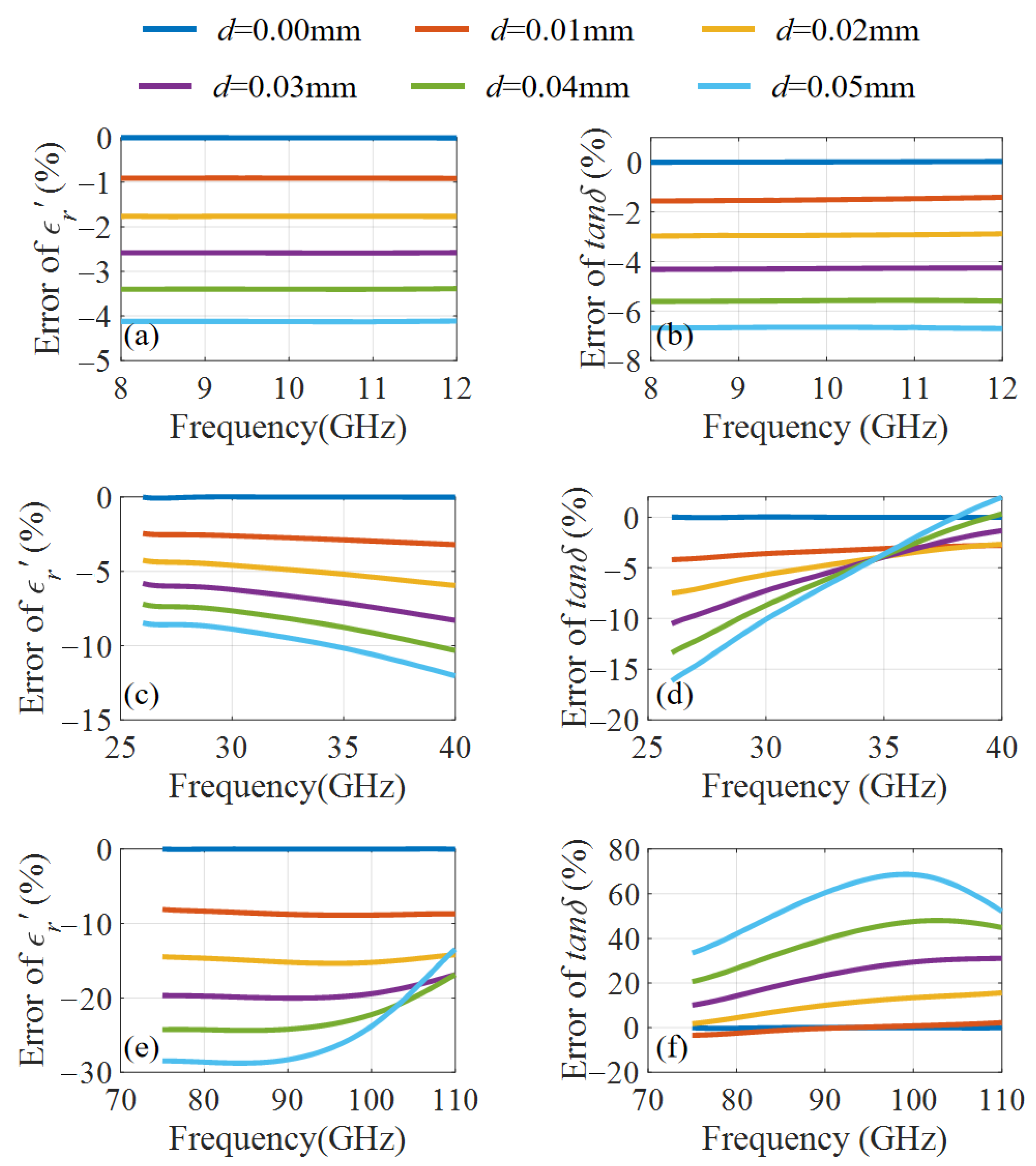
To simplify the analysis while maintaining its generality, we assume that the air gaps at the top and bottom ends are the same in simulation, i.e., d 1 = d 2 . In the following, a typical high-loss material with ϵ r = 15.0 and t a n δ = 0.5 is considered. The sample thickness is 1 mm. Figure 2 shows the errors of ϵ r and t a n δ in each band. It should be emphasized that the errors considered in this paper refer solely to those caused by the air gap. In Figure 2, d = d 1 + d 2 denotes the total air gap size. It can be seen that the air gap error will increase as the frequency increases. Specifically, for an air gap of 0.04 mm, the maximum error of ϵ r will increase from 3.4% to 24.4%, and the maximum error of t a n δ will increase from 5.6% to 48.1% when the measurement frequency is increased from the X to W band, respectively. In addition, it can be found that both ϵ r and t a n δ errors fluctuate considerably with frequency in the Ka and W bands. When the air gap is 0.04 mm, the errors for ϵ r can range from −24.4% to −16.8%, while the errors for t a n δ can vary from 20.6% to 48.1% between 75 GHz and 110 GHz. Additionally, the error will fluctuate more with frequency as d increases. Consequently, the measured trend of ϵ r and t a n δ with frequency may significantly differ from the actual situation. However, the knowledge of the correct trend of dielectric parameter variation with frequency will not only affect the design of dielectric-based devices but is also crucial for studying material dielectric and loss mechanisms. Therefore, the SWM should be improved to meet millimeter-wave measurement requirements.
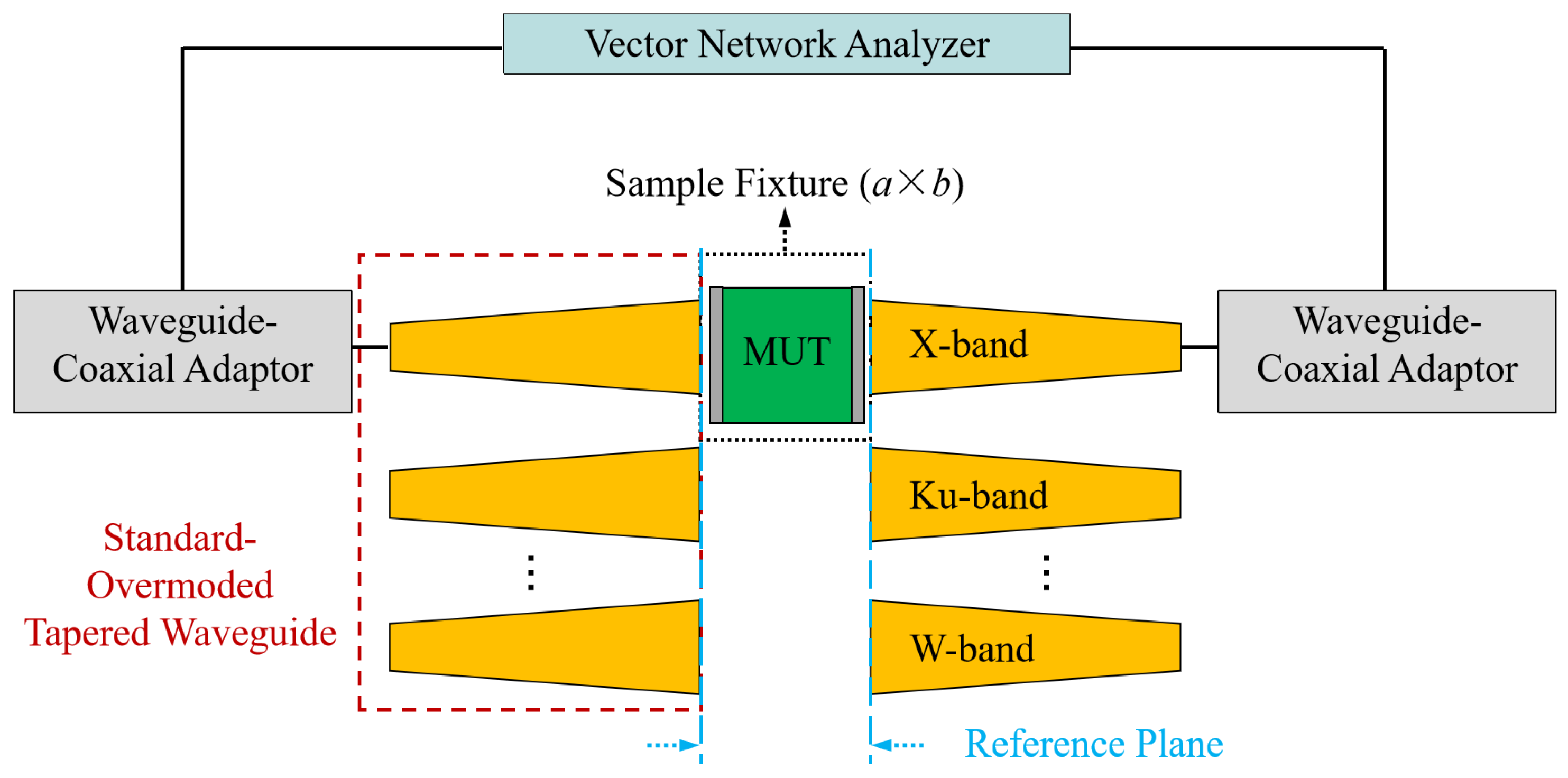
To achieve a broadband and high-accuracy permittivity measurement from 8 to 110 GHz, we proposed and designed an OWM-based measurement kit. Figure 3 shows the topology of the designed kit. It consists of seven pairs of standard-overmoded-waveguide transition structures (operating on X, Ku, K, Ka, Q, V, and W bands) and an overmoded rectangular waveguide sample fixture with dimensions of 22.86 mm × 10.16 mm. Therefore, only one sample with cross-section dimensions of 22.86 mm × 10.16 mm needs to be fabricated in the 8–110 GHz measurement band. The transition structure converts the standard waveguide TE 10 mode to the overmoded waveguide TE 10 mode. The through-reflect-line (TRL) calibration technique will be performed to de-embed the S-matrix of transition structures [19]. For this purpose, we designed the corresponding calibration kits for each band. The length of the “line” components are designed to be 9.8 mm, 5.7 mm, 3.6 mm, 2.4 mm, 2.0 mm, 1.5 mm, and 1.0 mm for each frequency band, respectively, to avoid the phase instability near 0° and 180°. The designed structure parameters are listed in Table 1. It should be noted that although the tapered transition structure is designed to guarantee high-purity transmission of the TE 10 mode (with mode purity > 99%), the introduced parasitic modes (such as TE 30 , TE 50 , TM 12 , etc.) can still can cause slight resonance and lead to unreasonable extraction results at specific frequencies [13,14]. To address this problem, it is necessary to perform post-processing steps to remove the resonance peaks. In material measurement, time-domain gating technologies or filtering algorithms (used in our work) are widely used, as presented in [20,21].
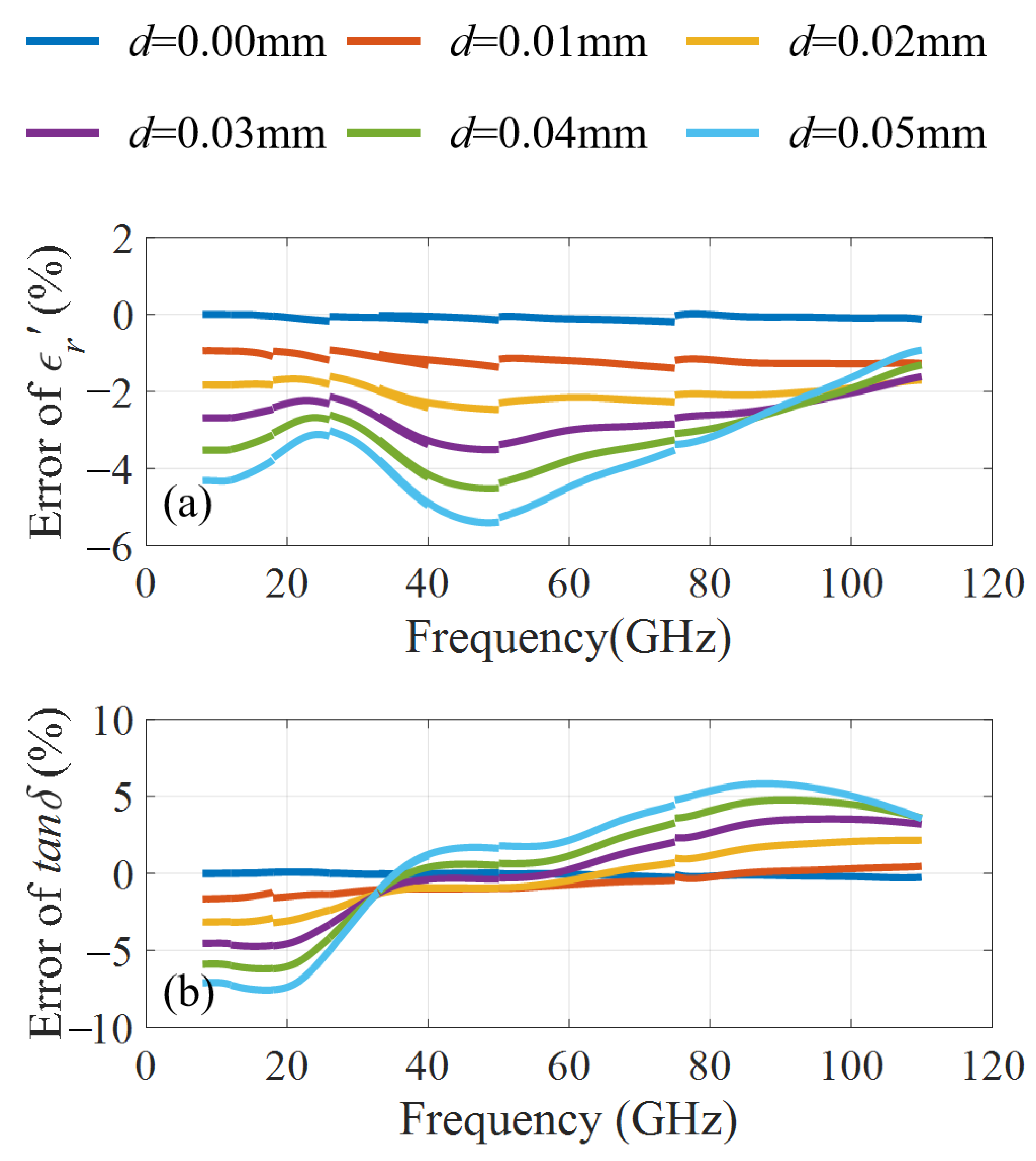
Based on the designed kits, we performed an error analysis of the material with ϵ r = 15 and t a n δ = 0.5 in Figure 4. It shows when d is smaller than 0.03 mm, the errors of ϵ r and t a n δ does not exceed 5% in 8–110 GHz. When the air gap d is increased to 0.05 mm, the errors of ϵ r and t a n δ can be significantly reduced from over 28% and 68% to within 6% and 8%, respectively, compared to SWM. In addition, the fluctuation ranges of ϵ r and t a n δ errors will be reduced from 24% and 75% to 5% and 13%, respectively, over the whole measurement band from 8 to 110 GHz. These results indicate that the designed OWM-based measurement kit is much more accurate than SWM and does not require sample replacement during measurement in different frequency bands. These excellent properties give the designed kit potential for a wide range of applications.

3. Measurement Results

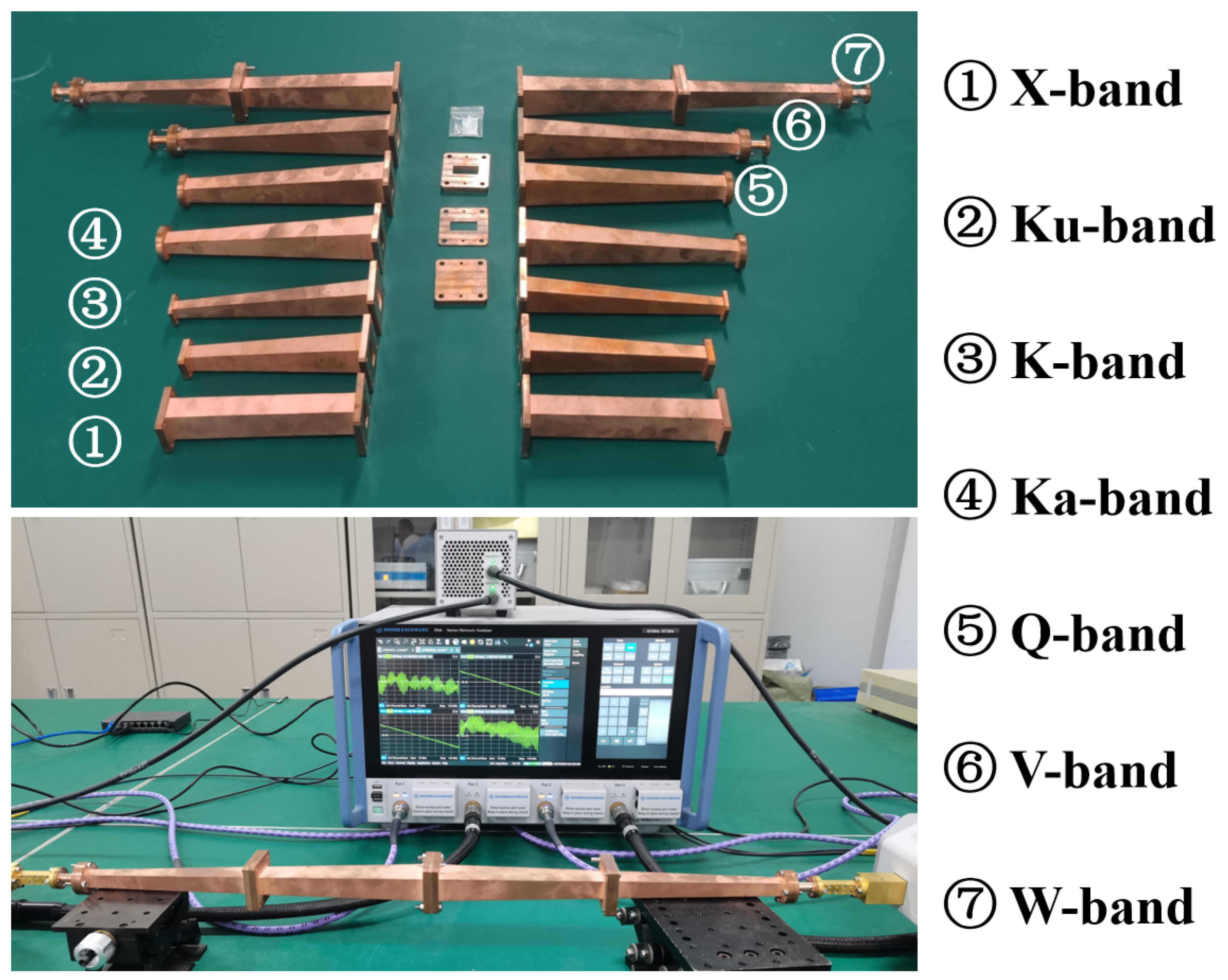
The experimental verification and application of the proposed measurement kit will be presented in this section. Figure 5 shows the vector network analyzer (VNA) measurement platform and the fabricated OWM-based kit. Although the waveguide method is more suitable for measuring high-loss materials, there is a lack of reported standardized data for the complex permittivity of high-loss materials to assess measurement accuracy. In order to verify the designed kit, we measured the well-known low-loss polytetrafluoroethylene (PTFE) and compared the measured results with reported data obtained by various broadband measurements. Furthermore, the OWM-based kit is applied to a high-loss BeO-TiO2 ceramic measurement.

3.1. Measurement Verification of the PTFE

In our measurement, the PTFE sample has a thickness of 1 mm. The measurement results are shown in Figure 6. It should be mentioned that due to the limitations of our laboratory equipment, we did not measure V-band (50–75 GHz). Nevertheless, since the measurement band is sufficiently wide, it does not affect our conclusion. From Figure 6 we can find that the average ϵ r and t a n δ is 2.02 and 0.001. Since the waveguide method does not yield an accurate t a n δ for low-loss materials ( t a n δ < 0.001), we just compare the extracted ϵ r with the reported data. The measurement results and reported data are summarized in Table 2. It can be seen that our measurement results agree well with the reported data in the 8–110 GHz range, which effectively verifies the feasibility of the OWM-based kit.

3.2. Application in Lossy Material Measurement

A high-loss BeO-TiO2 ceramic is measured using our designed measurement kit. It is produced of BeO ceramic with TiO2 powder [27]. The complex permittivity of the BeO-TiO2 ceramics can be adjusted by changing the proportion of BeO and TiO2. The ϵ r and t a n δ of BeO-TiO2 ceramics are typically in the range of 5–30 and 0.1–5. Due to its high-loss property, BeO-TiO2 ceramics are can be used in absorbers [28], power beam applications [2], and vacuum devices [29]. Since this material is susceptible to composition and sintering processes, it is necessary not to replace samples during broadband measurement in different frequency bands.
Figure 7 shows the measured ϵ r and t a n δ of the BeO-TiO2 ceramic. The BeO-TiO2 sample under measurement has a thickness of 1 mm. In Figure 7, the shaded area shows the uncertainties caused by VNA noise and repeated measurements. They are ±0.4 and ±0.005 for ϵ r and t a n δ , respectively. It can be found that both the ϵ r and t a n δ show a decreasing trend with the frequency. They decrease from 18.63 to 9.03 and 2.23 to 0.56 in 8–110 GHz, respectively. Since the measurement results in different frequency bands are consistent, these results can be considered credible. These data provide essential information for developing high-loss BeO-TiO2 ceramics and its application.

4. Conclusions

This paper presents an ultra-broadband OWM-based measurement kit operating in 8–110 GHz with high accuracy. Simulation analysis indicates the errors of ϵ r and t a n δ can be controlled within 6% and 8% with a large E-plane air gap of 0.05 mm for measurements of high-loss material. The PTFE sample is measured and compared with the published references to verify the designed kit. Then, it is applied in the measurement for high-loss BeO-TiO2 ceramic. Based on the simulation and measurement results, the proposed method is an effective solution for measuring ultra-broadband properties of the complex permittivity, which contributes to the study of dielectric mechanisms and the application of materials.

Author Contributions

W.W. proposed the conceptualization and methodology, and wrote the main manuscript text. G.S. and Y.C. conducted the simulations, experiments, and analysis. T.W., F.S., and S.F. fabricated the designed devices. X.T., X.L., and G.L. provided the samples and suggestions. All authors have read and agreed to the published version of the manuscript.

Funding

This work was supported by Sichuan Science and Technology Program under the grant No. 2024ZYD0153.

Data Availability Statement

All data are included in the manuscript.

Conflicts of Interest

The authors declare no conflicts of interest.

References

  1. Song, H.J.; Nagatsuma, T. Present and future of terahertz communications. IEEE Trans. Terahertz Sci. Technol. 2011, 1, 256–263. [Google Scholar] [CrossRef]
  2. Cohick, Z.W.; Schaub, S.C.; Hoff, B.; Dynys, F.W.; Baros, A.E.; Telmer, M.; Orozco, H.; Grudt, R.O.; Hayden, S.C.; Rittersdorf, I.M.; et al. High temperature W-band complex permittivity measurements of thermally cycled ceramic-metal composites: AlN:Mo with 0.25 to 4.0 vol% Mo from 25 °C to 1000 °C in air. IEEE Trans. Terahertz Sci. Technol. 2021, 33, 015901. [Google Scholar] [CrossRef]
  3. Calame, J.P.; Abe, D.K. Applications of advanced materials technologies to vacuum electronic devices. IEEE Trans. Terahertz Sci. Technol. 1999, 87, 840–864. [Google Scholar] [CrossRef]
  4. Chen, L.F.; Ong, C.K.; Neo, C.P.; Varadan, V.V.; Varadan, V.K. Microwave Electronics: Measurement and Materials Characterization; Wiley: West Sussex, UK, 2004. [Google Scholar]
  5. Wilson, S.B. Modal analysis of the ’gap effect’ in waveguide dielectric measurements. IEEE Trans. Microw. Theory Tech. 1988, 36, 752–756. [Google Scholar] [CrossRef]
  6. Foudazi, A.; Donnell, K.M. Effect of sample preparation on microwave material characterization by loaded waveguide technique. IEEE Trans. Instrum. Meas. 2016, 65, 1669–1677. [Google Scholar] [CrossRef]
  7. Yang, G.F.; Zhou, S.H.; Liang, W.; Li, X.; Huang, H.; Yang, J.H. Effect of different shapes on the measurement of dielectric constants of low-loss materials with rectangular waveguides at X-band. IEEE Microw. Wireless Compon. Lett. 2022, 32, 1471–1474. [Google Scholar] [CrossRef]
  8. Baker-Jarvis, J.R. Measuring Permittivity and Permeability of Lossy Materials: Solids, Liquids, Metals, and Negative-Index Materials; Technical Report; National Institute of Standards and Technology: Washington, DC, USA, 2005.
  9. Wang, W.J.; Jiang, W.; Yao, Y.L.; Wang, J.X.; Liu, G. An air gap correction method for permittivity extraction of high-loss materials. J. Electromagn. Waves Appl. 2024, 38, 1435–1449. [Google Scholar] [CrossRef]
  10. Wang, Y.; Hooper, I.; Edwards, E.; Grant, P.S. Gap-corrected thin-film permittivity and permeability measurement with a broadband coaxial line technique. IEEE Trans. Terahertz Sci. Technol. 2016, 64, 924–930. [Google Scholar] [CrossRef]
  11. Xu, H.; Liang, W.; Gao, Q. A self-gap-correction method for accurate permittivity measurement using the hybrid optimization algorithm. IEEE Trans. Instrum. Meas. 2019, 68, 1781–1787. [Google Scholar] [CrossRef]
  12. Wang, W.J.; Jiang, W.; Yao, Y.L.; Wang, J.X.; Liu, G. An improved waveguide method for accurate complex permittivity measurement of medium/high-loss material. Meas. Sci. Technol. 2024, 35, 066005. [Google Scholar] [CrossRef]
  13. Wang, W.J.; Liu, G.; Wang, Y.; Jiang, W.; Zheng, Q.; Wang, J.X.; Luo, Y. A more accurate measurement method of the dielectric material properties with high tolerance using an overmoded waveguide. IEEE Trans. Microw. Theory Tech. 2022, 70, 2363–2369. [Google Scholar] [CrossRef]
  14. Gong, X.Q.; Wang, W.J.; Liu, G.; Cao, Y.J.; Wang, Y.; Jiang, W.; Yao, Y.L.; Shu, G.X.; Wang, J.X.; Luo, Y. An improved overmoded-waveguide method for the accurate measurement of dielectric properties in the sub-terahertz band. J. Infrared. Milli. Terahz Waves 2023, 44, 265–280. [Google Scholar] [CrossRef]
  15. Wang, X.C.; Tretyakov, S.A. Fast and robust characterization of lossy dielectric slabs using rectangular waveguides. IEEE Trans. Microw. Theory Tech. 2022, 70, 2341–2350. [Google Scholar] [CrossRef]
  16. Choi, H.E.; Choi, W.; Simakov, E.I.; Zuboraj, M.; Carlsten, B.E.; Choi, E. Error tolerant method of dielectric permittivity determination using a TE01 mode in a circular waveguide at the W-band. IEEE Trans. Microw. Theory Tech. 2020, 68, 808–815. [Google Scholar] [CrossRef]
  17. CST-Computer Simulation Technology. Available online: http://www.cst.com/products/cstmws (accessed on 1 January 2025).
  18. Baker-Jarvis, J.; Vanzura, E.J.; Kissick, W.A. Improved technique for determining complex permittivity with the transmission/reflection method. IEEE Trans. Microw. Theory Tech. 1990, 38, 1096–1103. [Google Scholar] [CrossRef]
  19. Engen, G.F.; Hoer, C.A. Thru-reflect-line: An improved technique for calibrating the dual six-port automatic network analyzer. IEEE Trans. Microw. Theory Tech. 1979, 27, 987–993. [Google Scholar] [CrossRef]
  20. Wang, Y.; Shang, X.B.; Ridler, N.M.; Naftaly, M.; Dimitriadis, A.I.; Huang, T.D.; Wu, W. Material measurements using VNA-based material characterization kits subject to Thru-reflect-line calibration. IEEE Trans. Terahertz Sci. Technol. 2020, 10, 466–473. [Google Scholar] [CrossRef]
  21. Ma, D.D.; Shang, X.B.; Ridler, N.M.; Wu, W. Assessing the impact of data filtering techniques on material characterization at millimeter-wave frequencies. IEEE Trans. Instrum. Meas. 2021, 70, 6005904. [Google Scholar] [CrossRef]
  22. Baker-Jarvis, J. Transmission/Reflection and Short-Circuit Line Permittivity Measurements; National Institute of Standards and Technology: Gaithersburg, MD, USA, 1990.
  23. Abbas, Z.; Pollard, R.D.; Kelsall, R.W. Complex permittivity measurements at ka-band using rectangular dielectric waveguide. IEEE Trans. Instrum. Meas. 2001, 50, 1334–1342. [Google Scholar] [CrossRef]
  24. Wang, Y.; Shang, X.; Ridler, N.; Huang, T.; Wu, W. Characterization of dielectric materials at wr-15 band (50–75 ghz) using VNA-based technique. IEEE Trans. Instrum. Meas. 2020, 69, 4930–4939. [Google Scholar] [CrossRef]
  25. Choi, H.E.; Choi, E. High-precision complex permittivity measurement of high loss dielectric materials using a geometrical gap in millimeter wave frequency. J. Infrared Milli. Terahz Wave 2024, 45, 97–115. [Google Scholar] [CrossRef]
  26. Yamaguchi, Y.; Sato, Y. Measuring method of complex dielectric constant with monostatic horn antenna in w-band using multiple distance measurements and analysis. In Proceedings of the IEEE Asia–Pacific Microwave Conference (APMC), Kuala Lumpar, Malaysia, 13–16 November 2017; pp. 666–669. [Google Scholar]
  27. Kiiko, V.S.; Pavlov, A.V.; Bykov, V.A. Production and thermophysical properties of BeO ceramics with the addition of nanocrystalline titanium dioxide. Refract. Ind. Ceram. 2019, 59, 616–622. [Google Scholar] [CrossRef]
  28. Eichhorn, R.; Conway, J.; He, Y.; Li, Y.; O’Connel, T.; Quigley, P.; Sears, J.; Shemelin, V. Higher order mode absorbers for high current ERL applications. In Proceedings of the 5th International Particle Accelerator Conference, Dresden, Germany, 15–20 June 2014; pp. 4037–4039. [Google Scholar]
  29. Liu, G.; Jiang, W.; Yao, Y.L.; Wang, W.J.; Cao, Y.J.; Wang, J.X.; Luo, Y. High average power test of a W-band broadband gyrotron traveling wave tube. IEEE Electron. Device Lett. 2022, 43, 950–953. [Google Scholar] [CrossRef]
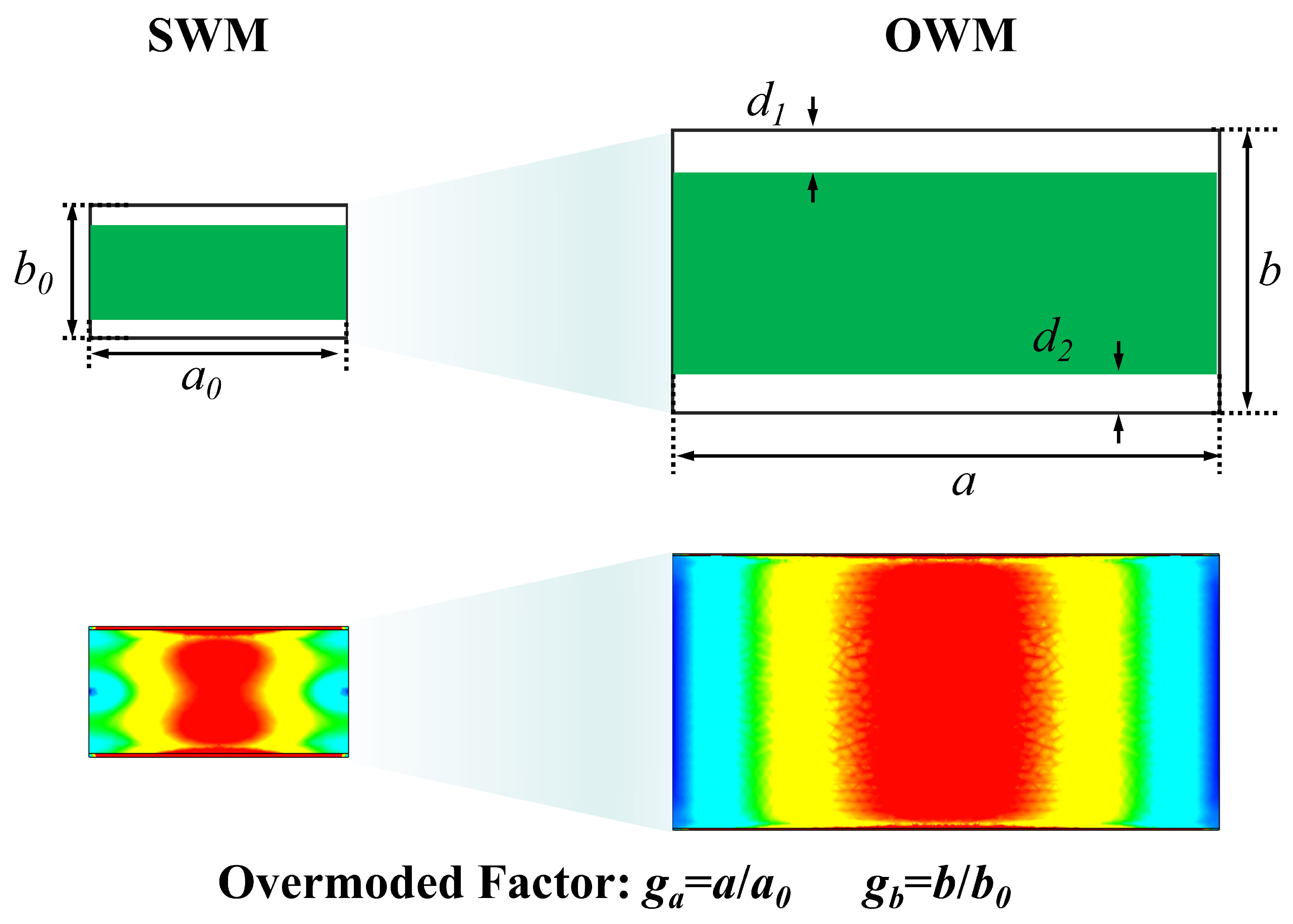
Figure 1. Electric field diagrams of the loaded fixture by SWM and OWM with the air gap.
Micromachines 16 01045 g001
Figure 2. Measurement errors of ϵ r and t a n δ in various frequency bands with different air gaps d. (a) errors of ϵ r at X–band, (b) errors of t a n δ at X–band, (c) errors of ϵ r at Ka–band, (d) errors of t a n δ at Ka–band, (e) errors of ϵ r at W–band, (f) errors of t a n δ at W–band.
Micromachines 16 01045 g002
Figure 3. Schematic diagram of the designed OWM-based measurement system.
Micromachines 16 01045 g003
Figure 4. Measurement errors of ϵ r and t a n δ in 8–110 GHz with different air gaps d. (a) errors of ϵ r ; (b) errors of t a n δ .
Micromachines 16 01045 g004
Figure 5. VNA measurement platform and the fabricated OWM-based kit.
Micromachines 16 01045 g005
Figure 6. Measurement results of the PTFE. (a) ϵ r , (b) t a n δ .
Micromachines 16 01045 g006
Figure 7. Measurement results of the BeO-TiO2 ceramic. (a) ϵ r , (b) t a n δ .
Micromachines 16 01045 g007
Table 1. Structure parameters of the OWM-based measurement kits.
Frequency BandXKuKKaQVW
Frequency Range (GHz)8–1212–1818–2626–4033–5050–7575–110
Overmoded Factor g a 11.452.143.214.026.089.00
Overmoded Factor g b 11.291.902.863.575.418.00
Taper length (mm)140140140160180250300
Line length (mm)9.85.73.62.42.01.51.0
Sample Fixture Size (mm)22.86 × 10.16 mm
Table 2. Reported permittivity of the PTFE.
ReferenceMeasurement Frequency ϵ r Measurement Method
[22]1–18 GHz2.03–2.04Coaxial Line
[23]26–40 GHz1.95Dielectric Waveguide
[24]50–75 GHz1.99–2.01Guided Free-space
[25]80–105 GHz1.99–2.00Circular Waveguide
[26]75–110 GHz2.05Free-space Method
This work8–110 GHz2.00–2.03OWM
Disclaimer/Publisher’s Note: The statements, opinions and data contained in all publications are solely those of the individual author(s) and contributor(s) and not of MDPI and/or the editor(s). MDPI and/or the editor(s) disclaim responsibility for any injury to people or property resulting from any ideas, methods, instructions or products referred to in the content.